Language selection

Search

Patent 2144420 Summary

Third-party information liability

Some of the information on this Web page has been provided by external sources. The Government of Canada is not responsible for the accuracy, reliability or currency of the information supplied by external sources. Users wishing to rely upon this information should consult directly with the source of the information. Content provided by external sources is not subject to official languages, privacy and accessibility requirements.

Claims and Abstract availability

Any discrepancies in the text and image of the Claims and Abstract are due to differing posting times. Text of the Claims and Abstract are posted:

  • At the time the application is open to public inspection;
  • At the time of issue of the patent (grant).
(12) Patent: (11) CA 2144420
(54) English Title: CIRCUIT ARRANGEMENT FOR AN INTEGRATED OUTPUT AMPLIFIER
(54) French Title: CIRCUIT POUR AMPLIFICATEUR A SORTIES INTEGREES
Status: Deemed expired
Bibliographic Data
(51) International Patent Classification (IPC):
  • H03F 3/45 (2006.01)
  • H03F 1/32 (2006.01)
  • H04R 25/00 (2006.01)
(72) Inventors :
  • ANDERSEN, HENNING HAUGAARD (Denmark)
(73) Owners :
  • TOPHOLM & WESTERMANN APS (Denmark)
(71) Applicants :
(74) Agent: G. RONALD BELL & ASSOCIATES
(74) Associate agent:
(45) Issued: 1997-10-14
(86) PCT Filing Date: 1993-11-06
(87) Open to Public Inspection: 1994-07-07
Examination requested: 1995-03-10
Availability of licence: N/A
(25) Language of filing: English

Patent Cooperation Treaty (PCT): Yes
(86) PCT Filing Number: PCT/EP1993/003109
(87) International Publication Number: WO1994/015397
(85) National Entry: 1995-03-10

(30) Application Priority Data:
Application No. Country/Territory Date
P 42 43 009.7 Germany 1992-12-19

Abstracts

English Abstract


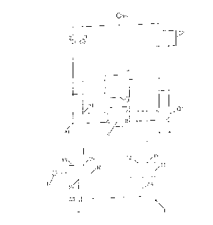
The invention relates to a circuit arrangement for an integrated output amplifier (1)
with two constant current sources (2, 3), a voltage amplifier with two inputs (5, 6)
and two outputs (7, 8) and two output transistors (Q1, Q2) coupled with these, as well
as two feedback networks (9, 10) producing negative feedback which are connectedbetween the output transistors and the corresponding input transistors of the voltage
amplifier (4). The first two feedback networks (9, 10) are connected between thecollectors of the output transistors (Q1, Q2) and the base electrodes of the
corresponding input transistors of the voltage amplifier (4). In addition, a third
feedback network (11) is connected on the input side to the base electrodes of the
output transistors and on the output side to the input of a current splitting network
(16) via a transistor (Q3) acting as a current sink, whereby said current splitting
network has a signal input (17). The current splitting network (16) has two parallel
branches (18, 19), between which the current flowing through this network can besplit, whereby this is controlled by the signal present at the signal input (17), and
whereby the branches (18 and 19) of the current splitting network (16) are connected
on the one hand with the constant current sources (2 and 3) and on the other hand
with the inputs of the voltage amplifier (4).


French Abstract

L'invention est un circuit pour un amplificateur intégré (1) qui comprend deux sources de courant constant (2, 3), un amplificateur de tension ayant deux entrées (5, 6) et deux sorties (7, 8) et deux transistors de sortie (Q1, Q2) couplés à ces dernières, ainsi que deux réseaux de réaction négative (9, 10) connectés entre les transistors de sortie et les transistors d'entrée correspondants de l'amplificateur de tension (4). Les deux premiers réseaux de réaction (9, 10) sont connectés entre les connecteurs des transistors de sortie (Q1, Q2) et les bases des transistors d'entrée correspondants de l'amplificateur de tension (4). Par ailleurs, l'entrée d'un troisième réseau de réaction (11) est connectée aux bases des transistors de sortie, alors que la sortie de ce réseau est connectée à l'entrée d'un réseau diviseur de courant (16) via un transistor (Q3) servant de puits de courant. Ce réseau diviseur de courant comporte une entrée de signaux (17) ainsi que deux branchements parallèles (18, 19) entre lesquels le courant interne est réparti; cette répartition est contrôlée par le signal présent à l'entrée (17) et les branchements (18, 19) du réseau diviseur de courant (16) sont connectés aux sources de courant constant (2, 3) d'une part et aux entrées d'un amplificateur de tension (4) d'autre part.

Claims

Note: Claims are shown in the official language in which they were submitted.


PATENT CLAIMS 1-3

1. Circuit arrangement for an integrated output amplifier (1), with two
essentially identical constant current sources (2, 3), a voltage amplifier (4)
with two inputs (5, 6) and two outputs (7, 8) and two essentially identical
output transistors coupled with these, as well as two essentially identical
feedback networks (9, 10) producing negative feedback which are connected
between the output transistors (Q1, Q2) and the assigned input transistors of
the voltage amplifier (4), characterized in that the output transistors (Q1, Q2)are actively driven at their base electrodes by the voltage amplifier (4), whilethe emitter electrodes are connected to ground and the collector electrodes to aload (22), in that the first two feedback networks (9, 10) are connected
between the collectors of the output transistors (Q1, Q2) and the base
electrodes of the corresponding input transistors of the voltage amplifier (4),
in that a third feedback network (11) which controls the closed-circuit current
is connected on the input side (12, 13) to the base electrodes of the output
transistors and on the output side (14) with the base electrode of a transistor
(Q3) acting as a current sink, whereby the emitter electrode of the latter is
connected with ground and the collector electrode with an input (15) of a
current splitting network (16), whereby said current splitting network is also
provided with a signal input (17), and in that the current splitting network (16)
has two parallel branches (18, 19) between which the current flowing through
this network can be split, whereby said current is controlled by the signal at
the signal input (17), and in that the branches (18 and 19) of the current
splitting network (16) are connected on the one hand with the constant current
sources (2 and 3) and on the other hand with the inputs (5 and 6) of the
voltage amplifier (4).


2. Circuit arrangement in accordance with claim 1, characterized in that one or
more of the feedback networks consist of passive, resistive components.

3. Circuit arrangement in accordance with claims 1 and 2, characterized in that
the output power of the output amplifier (1) can be limited to a lower value
than the maximum value by limiting the currents supplied by the constant
current sources (2, 3).

Description

Note: Descriptions are shown in the official language in which they were submitted.


, .1 ' 2144g20
-- 1
Circuit arrangement for an integrated output amplifler

The invention relates to a circuit arrangement for an integrated output amplifier with
two essentially identical constant current sources, an integrated voltage amplifier with
two inputs and two outputs and essentially identical output transistors coupled with
these, as well as two essentially identical negative feedback networks between the
output transistors and the correspondingly assigned input transistors of the voltage
amplifier.

Such highly integrated circuits are particularly suitable for output amplifiers with a
relatively low power output, such as those which can be used in hearing aids.

As is generally known, the gain normally changes greatly with the output current at
very low output impedances if the output-side load is a largely inductive load with a
DC resistance of 50 Ohm and an AC resistance at 800 Hz of around 100 Ohm.

Such a circuit is known, for example, from US PS 4 085 382. Here, a directly coupled
integrated class B amplifler with a low power rating is described, whereby this
consists of a three-stage two-channel pre-amplifier and a pair of output transistors,
one for each channel. A negative feedback loop is provided in each channel whichconnects the collector of the transistor in the last stage of the preamplil ler with the
base electrode in the first stage of the pre-amplifier and thus controls the direct
current level.

A negative, resistive AC voltage feedback loop connects the collector of one output
transistor in each case with the collector of the corresponding first pre-amplifier
transistor in order to reduce the gain dependence of the respective channel on the
current flowing through the output transistor. This is intended to reduce the closed-
circuit currents in the output transistors.

' 't' ~ - 2 - 214~420


However, these amplifiers have a relatively high gain of more than 40 dB.

~ . Object of the invention:

However, this circuit is not without problems. Firstly, it requires too many and too
large external components, e.g. two capacitors in the microfarad range and one
capacitor in the nanofarad range for stabilization.

In addition, the power requirement is too high and the output power obtained from
this is too low. Although it is always attempted to keep the closed-circuit current of
the output transistors as low as possible, high distortions are obtained for a load with
low impedance if this current is reduced too much. l he better the output transistors
are driven into the saturation region, the lower the amount of power tapped from the
voltage source which is lost in the amplifier.

In the known circuit, the output transistors are controlled passively, i.e. by a resistor,
and the level is kept low in order to limit the closed-circuit current. However, the
result of this is that the saturation of the output transistors is insufficient. In addition,
although the input-side noise is low with the known amplifier, the overall gain factor
is high (greater than 40 dB), and this means in turn that the signal-to-noise ratio is not
very good at a low gain setting.

It is not possible to reduce the gain of the output stage, however, since otherwise the
input stage will be driven into saturation before the output stage.

It is the object of the invention to improve a circuit arrangement of the type
mentioned above in such a way that it is possible to achieve a lower closed-circuit

~ 21~4~.2~

current with fewer external components and to obtain a high modulation capability
with low distortion for an average gain of e.g. 20 to 30 dB.

This is achieved by the invention through the characteristics of patent claim 1.

Further characteristics of the invention are described in the other patent claims.

The invention will now be described in greater detail on the basis of an exampleembodiment in conjunction with the enclosed drawings.

In the drawings,

Fig. 1 shows the gain characteristic at small signal amplitudes as a function of the
voltage applied to the load for two impedance values as the state of the art;

Pig. 2 shows a greatly simplified schematic diagram of the new output amplifier;

Fig. 3 shows a simplified schematic diagram of the output amplifier in accordance
with the invention and

Fig. 4 shows the gain characteristic for small signal amplitudes as a function of the
voltage applied to the load for two impedance values for a circuit designed in
accordance with the invention.

It is possible to see from the characteristic of the individual curves in Fig. 1 that the
differences between a load resistance of 50 Ohm and a load resistance of 500 Ohmare quite drastic. It must therefore be possible to improve this characteristic of an
output amplifier.

2144420
-- 4
Fig. 2 initially shows the greatly simplified schematic diagram of the invention. In
output amplifier 1, a voltage source Vs feeds two constant current sources 2 and 3,
which in turn feed a voltage amplifier 4 with two inputs 5 and 6 as well as two
outputs 7 and 8. This voltage amplifier drives two power transistors as output
transistors Q1 and Q2. In addition, two feedback networks 9 and 10 are connectedhere which are in turn connected with the conductors routed from the collectors of the
output transistors to the load. A further feedback network 11 is connected to the
output of the voltage amplifier and the conductors routed to the base electrodes of the
output transistors with the two inputs 12 and 13. In addition, a bias voltage source Vv
is also suggested.

The output 14 of the feedback network is connected with the base electrode of a
transistor Q3 functioning as a current sink. The emitter electrode of Q3 is connected
to ground. The collector of Q3 is connected to an input 15 of a current splitting
network 16. The latter also possesses a signal input 17. Two parallel conductors are
connected to the outputs 18 and 19 of this current splitting network, and these are
routed to the connection points 20 and 21 of the conductors from the constant current
sources. The output of the power transistors Q1, Q2 is connected with a load 22,which is preferably the primary winding of an output transformer provided with acenter tap.

This schematic diagram will now be explained in more detail with reference to Fig. 3,
whereby the same parts have the same reference numbers and therefore do not needrepeating.

The output amplifier has two almost identical constant current sources 2 and 3, a
current splitting network 16, two almost identical feedback networks 9 and 10, avoltage amplifier 4 with two inputs and two outputs, two almost identical output

' ~ 214~420
-- 5
transistors Q1 and Q2 as well as a further feedback network 11 and a transistor Q3
functioning as a current sink.

The constant current sources 2 and 3 supply a constant current to the nodal points 20
and 21. The transistor Q3 draws current to ground via the nodal point or input 15 of
the current splitting network, whereby the current is split between the two branches
18 and 19.

The splitting ratio is controlled by the input signal at the input terminal 17 in such a
way that the difference in the currents in the two branches 18 and 19 is proportional
to the signal present at the input terminal 17. If the signal amplitude at the input 17 is
high, the current flowing in the branch 18 goes to zero, while all the current ~owing
through the transistor Q3 flows through the branch 19. The opposite conditions are
obtained if there is a correspondingly high opposite signal amplitude at input 17, i.e.
all the current flowing through transistor Q3 will flow into branch 18, while branch
19 will not carry any current.

The voltage amplifier 4 has a non-inverting gain such that the total of the output
voltages is determined by the total of the input voltages. The amplifier also has a
differential gain such that the difference in the voltages at the outputs 7 and 8 is
determined by the difference in the voltages at the inputs 5 and 6.

The output transistors Ql and Q2 are controlled at their base electrodes, the emitter
electrodes are connected to ground and the collectors are connected to the load.

Negative feedback is realized by way of the feedback networks 9 and 10. Each of
these networks converts the voltage present at a collector into a current which is
supplied to the input of the voltage amplifier. This arrangement ensures that the
voltage across the load is proportional to the difference in the currents at the outputs


-

2144420
-- 6
18 and 19, thus guaranteeing the proportionality between the input signal and the
voltage across the load.

The feedback network 11 has two inputs 12 and 13 and one output 14. The output
voltage of this network is controlled by the average voltage of the input voltages at
the terminals 5 and 6, whereby there may be a small bias voltage.

The voltage present at output 14 of the feedback network is supplied to the base of
transistor Q3, whereby a transistor of the same type is used here, but this will very
probably be of a different order of magnitude than'Ql and Q2.

The feedback loop with the feedback network 11 controls the collector current of Q3
so that this current is the same as the total current from the constant current sources
2 and 3, plus the total of the currents originating from the feedback networks 9 and
10.

Since the voltage at the base electrode of Q3 is the same as the base voltages at the
output transistors Ql and Q2 when no input signal is present (possibly with a slight
shift), this voltage also controls the closed-circuit current of Q1 and Q2. If an input
signal occurs, the base voltages of Ql and Q2 deviate from the value of the closed-
circuit current by approximately the same values with opposite polarity.

In principle, this circuit initially functions without limitation of the output power at
the maximum possible power for the given operating voltage and subject to the
unavoidable limits placed by the circuit itself. However, such limitation of the output
power could be achieved by correspondingly limiting the currents supplied by theconstant current sources 2 and 3 . The voltage amplitude at the collector of Q 1 and Q2
is reduced if the current is set at a level which is not sufficient to produce the full
amplitude at the feedback networks 9 and 10.

~ 214~20


The output transistors can be driven into the saturation region if the currents supplied
by the constant current sources are high enough.

The transistors Q 1, Q2 and Q3 are represented as bipolar NPN transistors in theschematic circuit diagrams. The circuit would naturally also function in the same way
if PNP transistors were used, subject to a corresponding battery polarity, but NPN
transistors are normally better suited for integrated circuits.

The circuit arrangement would also function with N-channel or P-channel field effect
transistors.

The new circuit arrangement has fulfilled all the demands placed above, as has been
confirmed by tests and measurements.

First of all, it was possible to dispense with the large, external capacitors by not
limiting the output power under the maximum possible value. Such a limitation
could, for example, be achieved by limiting the currents supplied by the constant
current sources. In this case, a capacitor in the nanofarad range could be used if
required for decoupling.

If Fig. 1 is considered in this context, this demonstrates the behavior of a known
circuit connected to a load, which may consist, for example, of the primary winding
of an output transformer with a center tap.

The gain characteristic shows a deep dip at a low impedance of Z = 2 x 50 Ohm, such
as is obtained at low frequencies. In addition, the gain already drops steeply to both
sides at an amplitude of -0.6 V or ~ 0.6 V respectively

~ 2144~20

Fig. 4 shows the gain characteristic for the same impedances of Z = 2 x 50 Ohm and
Z = 2 x 500 Ohm such as can be achieved with an amplifier designed in accordancewith the invention. It is immediately possible to see that the overall gain is slightly
less than 30 dB, as demanded, and that this is true both for the low impedance of
Z = 2 x 50 Ohm as well as for the higher impedance of Z = 2 x 500 Ohm. Also, theamplitude of the AC voltage present at the transformer which produces a practically
identical gain differs only slightly for the two impedances.

This shows that it has been possible to meet the demand for balanced gain without
problems at both low impedances and high impedances, i.e. the circuit functions
practically free of distortion at low impedances as well.

Representative Drawing
A single figure which represents the drawing illustrating the invention.
Administrative Status

For a clearer understanding of the status of the application/patent presented on this page, the site Disclaimer , as well as the definitions for Patent , Administrative Status , Maintenance Fee  and Payment History  should be consulted.

Administrative Status

Title Date
Forecasted Issue Date 1997-10-14
(86) PCT Filing Date 1993-11-06
(87) PCT Publication Date 1994-07-07
(85) National Entry 1995-03-10
Examination Requested 1995-03-10
(45) Issued 1997-10-14
Deemed Expired 2008-11-06

Abandonment History

There is no abandonment history.

Payment History

Fee Type Anniversary Year Due Date Amount Paid Paid Date
Application Fee $0.00 1995-03-10
Registration of a document - section 124 $0.00 1995-10-19
Maintenance Fee - Application - New Act 2 1995-11-06 $100.00 1995-11-03
Maintenance Fee - Application - New Act 3 1996-11-06 $100.00 1996-10-29
Final Fee $300.00 1997-05-26
Maintenance Fee - Patent - New Act 4 1997-11-06 $100.00 1997-10-15
Maintenance Fee - Patent - New Act 5 1998-11-06 $150.00 1998-10-20
Maintenance Fee - Patent - New Act 6 1999-11-08 $150.00 1999-10-18
Maintenance Fee - Patent - New Act 7 2000-11-06 $150.00 2000-10-18
Maintenance Fee - Patent - New Act 8 2001-11-06 $150.00 2001-10-17
Maintenance Fee - Patent - New Act 9 2002-11-06 $150.00 2002-10-17
Maintenance Fee - Patent - New Act 10 2003-11-06 $200.00 2003-10-16
Maintenance Fee - Patent - New Act 11 2004-11-08 $250.00 2004-10-07
Maintenance Fee - Patent - New Act 12 2005-11-07 $250.00 2005-10-06
Maintenance Fee - Patent - New Act 13 2006-11-06 $250.00 2006-10-06
Owners on Record

Note: Records showing the ownership history in alphabetical order.

Current Owners on Record
TOPHOLM & WESTERMANN APS
Past Owners on Record
ANDERSEN, HENNING HAUGAARD
Past Owners that do not appear in the "Owners on Record" listing will appear in other documentation within the application.
Documents

To view selected files, please enter reCAPTCHA code :


To view images, click a link in the Document Description column. To download the documents, select one or more checkboxes in the first column and then click the "Download Selected in PDF format (Zip Archive)" or the "Download Selected as Single PDF" button.

List of published and non-published patent-specific documents on the CPD .

If you have any difficulty accessing content, you can call the Client Service Centre at 1-866-997-1936 or send them an e-mail at CIPO Client Service Centre.


Document
Description 
Date
(yyyy-mm-dd) 
Number of pages   Size of Image (KB) 
Cover Page 1995-08-23 1 16
Abstract 1994-07-07 1 33
Description 1994-07-07 8 296
Claims 1994-07-07 2 55
Drawings 1994-07-07 4 53
Representative Drawing 1998-01-06 1 4
Cover Page 1998-01-06 2 74
Cover Page 1998-01-21 3 122
Correspondence 1997-10-27 2 33
Fees 1997-10-15 1 52
Correspondence 1998-01-21 2 69
Fees 1995-11-03 1 47
Fees 1996-10-29 1 58
National Entry Request 1995-03-10 6 211
International Preliminary Examination Report 1995-03-10 41 1,330
Office Letter 1995-03-10 1 29
Office Letter 1996-12-03 1 95
Correspondence Related to Formalities 1997-05-26 1 32
Office Letter 1995-10-19 1 25