Note: Descriptions are shown in the official language in which they were submitted.
92-AIL-374
SHAPED DIGITAL NOISE GENERATOR AND METHOD
BACKGROUND OF THE INVENTION
Field of the Invention
This invention relates to a noise generation method
and system, and more particularly to a shaped digital
noise generation method and system.
Description of the Prior Art
Conventionally, digital noise generation is
l0 implemented by sampling an analog noise source, such as a
noise diode, i.e., sampling white noise. However, digital
noise generated by sampling white noise generally results
in several undesirable effects. For example, analog noise
sources display inconsistent unit-to-unit operation and
relatively high failure rates, requiring frequent
readjustments. In addition, thermal sensitivity inherent
in analog noise sources may affect the consistency of the
performance of the noise source rendering the quality of
digital noise generated therefrom inconsistent over time.
Conventional digital noise generation also includes a
method whereby multiple parallel taps off a single linear
feedback shift register are used to develop a sequence of
random digital word signals. The sequence of random
digital word signals is provided to a frequency modulating
synthesizer which translates the sequence to a digital
noise signal. The frequency of the digital noise signal
vary with each new word signal of the sequence. This
approach, however, like the technique that consists of
directly sampling white noise, has drawbacks. For
example, varying the frequency of a digital noise signal
in accordance with a generated sequence of digital word
signals may produce an even frequency distribution with an
~~~~~o~
-2-
uneven frequency rate distribution within the noise signal
generated thereby. More specifically, the frequency rate
distribution within the digital noise signal will reflect
a gaussian rather than flat character for a particular
frequency bandwidth mapped by the generated sequence.
Thus, a desirable flat crossing rate distribution will not
appear in the noise distribution and the power spectral
density of the generated noise signal.
OBJECTS AND SUMMARY OF THE INVENTION
It is therefore an object of the present invention to
provide a digital noise generation method and apparatus
which avoid the inconsistent unit-to-unit operation
prevalent in conventional digital noise generators
utilizing analog noise sources.
It is another object of the present invention to
provide a digital noise generation method and
apparatus which avoid the relative high failure rate and
frequent readjustment needs of conventional digital noise
generators utilizing analog noise sources.
It is yet another object of the present invention to
provide a digital noise generation method and apparatus
which provide a noise output signal having a uniform noise
distribution and power spectral density over a given
frequency range independent of environmental variations.
It is still another object of the present invention
to provide a digital noise generation apparatus for
generating high quality, evenly distributed digital noise
with increased reliability and reduced size and power
requirements.
CA 02144708 1999-02-02
-3-
An apparatus of the present invention for generating
a digital noise signal, the digital noise signal
characterized by a substantially evenly distributed
frequency content for substantially the entire frequency
_ bandwidth of the noise signal includes a digital word
signal generator for generating a random sequence of N-bit
digital word signals, each word signal being generated
with each cycle of a system clock signal that is provided
to the digital word signal generator. With respect to the
N-bit digital word signal, N is a non-zero integer and
each N-bit digital word signal represents an equivalent
decimal value in a range of possible values from 0 to (2"-
1) .
The digital noise signal generator also includes a
shaping circuit which transforms the random sequence of
digital word signals into a shaped sequence of N-bit
digital word signals. A frequency synthesizer is
responsive to each digital word signal of the shaped
sequence and provides the digital noise signal in response
to the digital word signals.
In one embodiment, each N-bit digital word signal of
the shaped sequence corresponds to a memory address within
a block of memory. Each memory address contains a stored
digital word signal that defines one portion of the
digital noise signal for one cycle of a system clock
signal. The frequency synthesizer is responsive to each
stored digital word signal.
In another embodiment of the invention, the shaping
circuit may include a subtracter for expanding the range
of values that each N-bit digital word signal of the
shaped sequence may represent. The range of possible
values may be expanded from about -(2"-1) to about (2"-1).
CA 02144708 1999-02-02
-4-
A method of the present invention for generating a
digital noise signal characterized by an evenly
distributed frequency content over a particular frequency
' bandwidth includes a step of generating a random sequence
of N-bit digital word signals within a sequence signal
generator, where each N-bit digital word signal is
generated with each cycle of a system clock signal. N is
a non-zero integer and a range of possible decimal
equivalent values representable by each N-bit digital word
signal extends from 0 to (2"-1).
The method includes the step of transforming the
random sequence of N-bit digital word signals into a
shaped sequence of N-bit digital word signals within a
shaping circuit. A frequency synthesizer generates a
portion of the digital noise signal in accordance with
each digital word signal of the shaped sequence. The
frequency of the digital noise signal vary with each cycle
of the system clock signal.
In one embodiment, the method may include the step of
translating the shaped sequence by retrieving a digital
word signal representing a frequency scaling factor, each
frequency scaling factor being stored at each of a
plurality of memory addresses within a block of memory.
Each memory address corresponds to a corresponding digital
word signal of the shaped sequence. Each digital word
signal representing each frequency scaling factor may be
utilized by the frequency synthesizer to generate the
digital noise signal. _
These and other objects, features and advantages of
this invention will become apparent from the following
detailed description of illustrative embodiments thereof,
which is to be read in conjunction with the accompanying
drawings.
21~4'~~8:,
-5-
BRIEF DESCRIPTION OF THE DRAWINGS
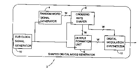
Figure 1 is a block diagram of a shaped digital noise
signal generator of the present invention.
Figure 2 is a block diagram of a random word signal
generator, one element of the shaped digital noise signal
generator of the present invention.
Figure 3 is a plot of power versus frequency of a
digital noise output signal generated using an unshaped
sequence of digital word signals provided by the present
to invention.
Figure 4 is a plot of crossing rate versus spot width
bin, each bin correlated to a corresponding digital word
signal of an unshaped sequence of digital word signals
provided by a sequence signal generator.
Figure 5 is a plot of crossing rate versus spot width
bin, each bin correlated to a corresponding digital word
signal of a shaped sequence of digital word signals
provided by a sequence signal generator of the present
invention.
Figure 6 is a circuit diagram of a sequence signal
generator of the present invention.
Figure 7 is a schematic block diagram of one
embodiment of a shaped digital noise signal generator of
the present invention.
Figure 8 is a circuit diagram of a sequence signal
generator of the present invention combined with a six-bit
signal subtracter.
2~.~4"~~$
-6-
Figure 9 is a schematic block diagram of another
embodiment of a shaped digital signal noise generator of
the present invention.
Figure 10 is a schematic block diagram of yet another
embodiment of a shaped digital signal noise generator of
the present invention.
DETAILED DESCRIPTION OF THE PREFERRED EMBODIMENTS
A digital noise signal generator 2 formed in
accordance with the present invention is shown in Figure
1. Digital noise signal generator 2 includes a random
word signal generator 4 and a crossing rate shaper 6 to
which the random word signal generator is electrically
connected. Random word signal generator 4 generates and
outputs a sequence (WI)~ of N-bit digital word signals WI,
where N is a non-zero integer defining the number of bits
contained in each digital word signal; "I" indicates
"input", and "J" represents incremental integer values.
Each N-bit digital word signal of sequence (WI)~ is
used to define a frequency or frequency rate value of a
portion of a digital noise signal output by the digital
noise signal generator 2. The crossing rate shaper 6
provides a function by which the sequence of digital word
signals (WI)~ generated within the random word signal
generator 4 may be transformed into a second, shaped
sequence (Wo)~. The "O" of Wo indicates that the shaped
sequence is the "output". The shaped sequence of digital
word signals (Wo)~ is the basis of the digital noise signal
provided by this invention.
The digital noise signal generator 2 of the present
invention also includes a digital modulation signal
synthesizer 12. The shaped sequence of digital word
signals (Wo)~ that is output from the crossing rate shaper
214470$
6 may be directly input into the digital modulation signal
synthesizer 12 in which the digital noise signal is
generated. Alternatively, the digital noise signal
generator 2 of the present invention may include an output
formation unit 8 (to be discussed below). The shaped
sequence (Wo)~ is further adjusted within the output
formation unit 8 prior to its input to the digital
modulation signal synthesizer 12.
The shaped sequence of digital word signals (Wo)~
provides for a more uniform frequency crossing rate
distribution within the generated digital noise signal as
compared to a frequency crossing rate distribution of a
digital noise signal generated in response to an unshaped
sequence (WI ) ~ .
A preferred form of the random word signal generator
4 is shown in Figure 2. The random word signal generator
preferably includes six (i.e., N = 6) linear feedback
shift registers 16, 18, 20, 22, 24, 26. Each linear
feedback shift register preferably includes 31 storage
units (registers) interconnected to define unique feedback
paths resulting in an ability to generate a sequence of 23'
unique 1-bit output signals. The sequence of 1-bit
signals generated by each linear feedback shift register
is repeated only after 23' cycles of a clock signal applied
thereto, i.e., each linear feedback shift register has a
repeat periodicity of 23' bits. Random word signal
generator 4 provides therefore one N-bit word signal WI of
a sequence of digital word signals (W1)~ with each clock
cycle applied thereto. A statistical distribution of the
26 possible values (where N=6) that each word signal WI may
assume is essentially uniform over the common repeat
period.
~1~4'~~g
_$_
Referring to Figure 1, the digital noise signal
generator 2 of the invention may further include a sub-
clock signal generator 10. The sub-clock signal generator
is electrically connected to the random word signal
5 generator 4, the crossing rate shaper 6 and the output
formation unit 8 to synchronously clock the random word
signal generator 4, the crossing rate shaper 6 and the
output formation unit 8.
Sub-clock signal generator 10 provides a system clock
10 signal that shifts each N-bit (i.e., six-bit) word signal
Wj generated within the random word signal generator 4
into the crossing rate shaper 6. Concurrently, a six-bit
digital word signal Wo of a shaped sequence of digital word
signals (Wo)~ generated by the crossing rate shaper is
shifted out of the crossing rate shaper 6 into the digital
modulation signal synthesizer 12. In an embodiment using
the output formation unit 8, each word signal output from
the crossing rate shaper 6 is shifted into the output
formation unit 8 where a subtracting function is
performed. Concomitantly, a word signal that is a product
of the subtracting is shifted from the output formation
unit 8 into the digital modulation signal synthesizer 12.
The sub-clock signal generator 10 preferably also
provides options to a user for selecting subdivisions of a
master clock contained within the sub-clock signal
generator. Varying the selected subdivision varies the
frequency of the system clock signal. The time variation
of the sequence of digital word signals (WI)~ output from
the random word signal generator 4, i.e., the repeat
periodicity, is directly proportional to the frequency of
the system clock signal provided by the sub-clock signal
generator 10. Table 1 defines a time duration of each
sequence of digital word signals (WI)~ output according to
the varying frequency of the clock signal.
_g_
TABLE 1
STAGES CODE LENGTH CLOCK TIME DURATION
OF LFSRs OF EACH SEQUENCE FREQUENCY (PERIODICITY)
31 2,147,483,647 20 MHZ 1.8 min
31 2,147,483,647 10 MHZ 3.6 min
31 2,147,483,647 1 MHZ 35.8 min
31 2,147,483,647 500 KHZ 72.0 min
In one embodiment, each six-bit digital word signal Wo
corresponds to a memory location within a memory block
(Figure 10). The block of memory may reside within the
crossing rate shaper 6 or the output formation unit 8, but
is not limited to being located at those locations. Each
memory location contains a digital word signal that
defines a frequency or a frequency rate value for a
portion of the digital noise signal. Each one-cycle
portion of the digital noise signal is a result of a
shifting of the memory-stored digital word signal
(corresponding to each N-bit digital word signal Wo) into
the digital modulation signal synthesizer 12. The
frequency and magnitude of the digital noise signal output
from the digital modulation signal synthesizer 12 changes
from a frequency or a frequency rate defined by a former
memory-stored digital word signal at an address
corresponding to word signal (Wo)~_~ to the frequency or a
frequency rate defined by a present memory-stored digital
word signal at an address corresponding to word signal
(wo)~.
The frequency of the digital noise signal may be
changed in discrete frequency amounts or may be changed
substantially continuously. If the frequency values
change substantially continuously, all frequency values
between the present and former frequencies are crossed or
passed through, i.e., a chirp signal is generated. Since
all frequency values are crossed, i.e., passed through in
.~ ~1447~~
-10-
either an increasing or decreasing frequency direction as
the frequency changes, the frequency rate distribution
within a digital noise signal is non-uniform when
generated from a random or unshaped sequence (WI)~ of
digital word signals. In other words, because all the
frequencies between each frequency value defined by each
digital word signal within any sequence are included in
the spectrum of the generated noise signal, random word
signal generation in a conventional system produces an
uneven frequency rate distribution resulting from the
over-representation of the crossed middle frequencies.
Figure 3 shows a power spectral plot versus frequency
of a digital noise signal generated in accordance with an
unshaped sequence of six-bit digital word signals (WI)~.
The digital noise signal shown in Figure 3 has a 100 MHz
spot width, or frequency bandwidth, the spot width
extending between 50 and 150 MHz. The power level of the
generated digital noise signal varies within the 100 MHz
spot width approximately 10 dB with varying frequency.
The range of decimal equivalent values spanned by
each six-bit digital word signal WI of an unshaped sequence
is from 0 to 63. Each of the 64 (i.e., 2") possible values
of each word signal Wt may be thought of as corresponding
to one of 64 possible bins. That is, each word of a
sequence of digital word signals (Wj)~ designates a
corresponding bin or 1/64 of a total space (e.g., in a
frequency spectrum) mapped by the 64 bins.
As in the embodiment discussed above, the 64 bins may
each map to one of 64 memory locations within a block of
memory addressable by the sequence of digital word
signals. The 64 memory locations may be contiguous.
More specifically, each sequence of digital word
signals, either an unshaped sequence of digital word
~I4~"~~8
-11-
signals (WI)~, or a shaped sequence of digital word signals
(Wo)~, corresponds to a sequence of bins. The sequence of
bins (defined by the sequence of word signals) may
represent a frequency value of the digital noise signal or
the sequence of bins may represent each address within a
block of memory as described above. The breadth of the 64
bin-defined frequency values defines a frequency bandwidth
(or noise spot width) for the digital noise output signal.
The noise spot width may be varied in size from the above-
mentioned 100 MHz value without departing from the scope
or spirit of the present invention.
Each new digital word signal (Wo or W~) changes a
designated bin (corresponding to a frequency value or an
address within a block of memory). The bins lying between
a former designated bin, e.g., a digital word signal (Wo)~_
~, and a presently designated bin, e.g., a digital word
signal (Wo)~, must be crossed (as would all the
corresponding frequencies or addresses therebetween) with
the generation of each new word signal corresponding to
each bin, i.e., the middle bins are crossed over. Thus,
as each middle bin between a former and present bin is
crossed, each frequency value or address corresponding
thereto is incorporated within the generated noise signal.
Figure 4 is a plot of crossing rate in MHz per bin,
where each bin corresponds to each digital word signal of
an unshaped sequence (WI)~ generated by means available in
the prior art. The crossing rate that results from the
unshaped sequence (WI)~ may be used by the invention to
provide a sequence of frequency values defining a noise
signal in which the middle frequency values are
represented more frequently than the outer frequency
values. The sequence of digital word signals (WI)~
therefore establishes the basis for a non-uniform
frequency rate distribution within the generated noise
signal.
2~44'~~~
-12-
In order to avoid the non-uniform frequency rate
distribution, the present invention includes the crossing
rate shaper 6. The crossing rate shaper 6 is preferably a
digital circuit that uniquely transforms (i.e., maps) each
digital word signal (corresponding to each bin) of a
sequence (W~)~ received from the random word signal
generator 4. The mapping is in accordance with shaping
logic (shown in Table 2) contained within the crossing
rate shaper. The shaping logic addresses the problem of
non-uniformity in the frequency rate distribution that
typifies conventional digital noise generated signals.
The generation of an unshaped sequence of digital
word signals for use in generating a noise signal
corresponding thereto is old in the art. It should be
noted, however, that although the digital noise generator
of the present invention has its basis in its ability to
provide a shaped sequence of digital word signals from an
unshaped sequence, the present invention can also provide
a noise signal generated according to the unshaped
sequence of digital word signals.
Figure 5 is a plot of crossing rate per bin that is
defined by a shaped sequence of digital word signals (Wo)~
provided by the crossing rate shaper 6. The mapping or
shaping logic within the crossing rate shaper 6 operates
to identify each digital word signal WI corresponding to
the more frequently crossed bins, and minimizes passing
through or accessing those bins in favor of bins that are
less frequently crossed. The bins that are less
frequently crossed are not skipped but are now accessed
more frequently by the shaping logic of the crossing rate
shaper 6. Accordingly, a more uniformly defined rate at
which all bins are crossed is provided as illustrated in
Figure 5 (compare with Figure 4).
2144'~~8.;
-13-
In another embodiment of the invention, the digital
modulation signal synthesizer 12 may include a block of
addressable memory (not shown). Each digital word signal
Wo of sequence (Wo)~ corresponds to one of each of 64
distinct memory locations within the block of memory. A
digital word signal stored at each memory location may
represent a frequency value, or a frequency rate (slope)
value, for some portion of the digital noise signal.
Thus, a new digital word signal Wo input to the digital
modulation signal synthesizer 12 with each cycle of the
clock signal causes a new memory-stored frequency rate or
frequency value to be accessed. The memory-stored
frequency values (or frequency slope values) are supplied
to the frequency modulation signal synthesizer 12 which
generates the digital noise signal accordingly. The
frequency of the digital noise signal
preferably changes substantially linearly with each cycle
of the clock signal, but may also change in discrete
steps.
TAHhE 2
WI
(ki) ~ 25 24 23 22 2t 2o I 25 24 23 22 2t 20
k3 0 1 0 0 X X 0 0 0 0 X X
k2 0 1 0 1 X X 0 0 0 0 X X
kt 0 1 1 0 X X 0 1 0 0 X X
k~ 0 1 1 1 X X 1 0 0 1 X X
1c0 1 0 0 0 X X 0 1 1 0 X X
kt 1 0 0 1 X X 1 0 1 1 X X
k2 1 O l O X X 1 1 1 1 X X
k3 1 0 1 1 X X 1 1 1 1 X X
~~~.~4"~Q8
-14-
Table 2 above illustrates the preferred shaping logic
of crossing rate shaper 6. The shaping logic defines a C-
bit, e.g., 2-bit, channel in the least significant bit
positions of each six-bit word signal WI input to the
crossing rate shaper. An "X" within Table 2 designates a
"don't care" stag for each particular bit position within
the C-bit channel of each N-bit digital word signal WI. C
may be any integer value from 0 to N. The two-bit channel
defined in Table 2 corresponds to a subspace S which
varies in decimal equivalent values from 0 to 3.
The C-defined portion of digital word signal WI, that
is, the subspace S, is not affected by the shaping logic
of the crossing rate shaper 6. The C least significant
bits of digital word signal WI, therefore, vary freely in
the shaped digital word signal Wo output. The other (N-C)
bits of WI that are not included within the subspace S,
i.e., the 4 most significant bits, are accordingly held
constant or forced to change with each word signal input
to the crossing rate shaper 6 by its internal shaping
logic.
If digital word signal Wj input to crossing rate
shaper 6 falls within one of the eight values defined by
Table 2, the 4 most significant bits are changed to the 4
most significant bits of the corresponding digital word
signal Wo. Table 2 entries (i.e., bit values) that are
designated by X ("don't care") identify those bits of
each digital word signal Wlthat are allowed to vary
freely, i.e., are provided at the output of the crossing
rate shaper 6 exactly as they are input. The four most
significant bits of digital word signal WI designated by
each k~ in the table represent constrictive sections or
subspaces within the 64 bin range.
2~.~4'~~8
-15-
The 2 least significant bits of each digital word
signal representing each of the 16 bins (i.e., 2~6-c~ or 24
bins that are defined by the four most significant bit
positions of each digital word signal) correlate to a bin
range or subspace. The 4 most significant bits of each
digital word signal Wo define the bin representing each
frequency value. Accordingly, the frequency of the shaped
digital noise signal will either change to a value defined
by WI or will be skipped to a frequency value defined by
the internal logic of the crossing rate shaper.
At least four different sequences (providing a basis
for four distinct variable digital noise signals) are
available with the different embodiments of this
invention. One of the first possible sequences of digital
word signals represents a sequence of six-bit uniformly
distributed shaped random numbers. A second possible
sequence of digital word signals represents a sequence of
six-bit unshaped or random numbers. A third possible
sequence of digital word signals represents a sequence of
seven-bit (two's complement) successive differences of
shaped random numbers and a fourth sequence of digital
word signals represents a sequence of seven-bit (two's
complement) successive differences of unshaped random
numbers.
The biasing rules (as manifest by Table 2) may
institute different dwell durations for each constrictive
section or subspace. That is, the crossing rate shaper 6
may cause a particular number of consecutive digital word
signals Wo to be restricted to one particular subspace.
For example, the decimal equivalent values represented by
each digital word signal Wo may be forced to vary between
32, 33, 34 and 35 for 512 clock cycles. These different
dwell durations are identified by an index k~ extending
from 0 to (W-C-1). For example, with W = 6 bits and C = 2
bits, the index would extend from 0 to 3 defining four
~1r~4'~08
-16-
channelized constrictive durations of k: ko, k~, kz and k3.
If k~ is held to one, there is a one-to-one correspondence
between a value represented by digital word signal WI that
was generated within the random word signal generator 4
and a value represented by digital word signal Wo that was
generated within the crossing rate shaper 6.
Thus, in this example, each constrictive section or
bin range corresponds to four decimal equivalent values
within a number of possible ranges of from 0 to 24 (16 bin
ranges), multiplied by C2 (22). The possible bin values
are 0, 4, 8, 12, 16, 20, 24, 28, 32, 36, 40, 44, 48, 52,
56 and 60 and the possible bin range extends 1, 2 or 3
units from the bin values.
The index i for each constrictive section (k~)
identifies which of the 16 constrictive sections or
channels defined by Table 2 will be held for a particular
dwell duration. For example, Table 2 identifies an index
varying from 0 to 3 for the eight possible values of k
(corresponding to eight possible channels or 2 bit-defined
subspaces) in each half of a mapping space. The mapping
space corresponds to the portion of Table 2 in which some
portion of the 64 possible bins are represented. For
example, with the sixth bit of a digital word signal WI
equal to 0, the upper half of the mapping space of Table 2
is accessed. With the sixth bit of a digital word signal
WI equal to 1, the lower half of the mapping space of Table
2 is accessed. Each constrictive channel or bin range may
vary only within the C-defined subspace S, i.e., the least
significant bits of the digital word signal.
As previously described with reference to Figure 1,
the signal output from the crossing rate shaper 6 (i.e.,
digital word signal (Wo)~) may be passed through an output
formation unit 8 prior to its transfer to the digital
modulation signal synthesizer 12. Output formation unit 8
~I4~'~~~
-17-
provides an additional function for shaping the shaped
sequence of digital word signals (Wo)~. Each digital word
signal Wo input to the output formation unit 8 may be
subtracted from a digital word signal Wo input with the
previous clock cycle (or vice versa). That is, digital
word signal (Wo)~+~ may be subtracted from digital word
signal (Wo) ~ .
The subtraction provides the output formation unit 8
with the ability to extend or expand the range of the 64
possible decimal equivalent values of each digital word
signal Wo input to the digital modulation signal
synthesizer 12. For example, the range of the sequence
of values may be extended from a span of 2" to a span
extending from about -(2"-1) to about (2"-1) using output
formation unit 8.
Each subtraction result formed by the output
formation unit 8 represents a memory location at which is
stored a frequency slope value designating a negative or
positive linear change in frequency. With each new
frequency slope value, the digital modulation signal
synthesizer 12 can provide a portion of a digital noise
signal in which the frequency changes according to the
frequency slope value for the clock cycle. If the
frequency slope value is negative, the frequency is
preferably decreased at the defined rate for the clock
cycle. If a frequency slope value is positive, the
frequency preferably increases at the defined rate for the
clock cycle.
The output formation unit 8 therefore allows the
present invention to provide a portion of a digital noise
signal that embodies a positive or negative change in
frequency for each clock cycle. The noise generated by
such a scheme enjoys a more even frequency crossing rate
content.
-18-
Referring to Figure 6, a circuit diagram of a
sequence signal generator 100 representing one embodiment
of this invention will now be described. The sequence
signal generator 100 includes a random word signal
generator 101 and a crossing rate shaper 114. The
sequence signal generator 100 can provide either a shaped
(Wo)~ or unshaped (WI)~ sequence of digital word signals.
The sequence signal generator 100 does not in and of
itself generate the digital noise signal, but merely
generates shaped or unshaped sequences representative of
the digital noise signal.
One form of sequence signal generator 10o is depicted
in Figure 6. The sequence signal generator was developed
using a programmable gate array, i.e., a XILINXTM XC3064
132 pin plastic grid array manufactured by Xilinx
Corporation of California. The sequence signal generator
implemented thereby consists of 2589 gates, with a total
measured power consumption of less than 1 watt. The
development of the desired noise signal specification
using the XILINXTM gate array was accomplished using a
clock rate ranging from about 500 KHz to about 20 MHz.
The random word signal generator 101 contained within
the sequence signal generator 100 preferably includes six
linear feedback shift registers 102, 104, 106, 108, 110,
112. The six linear feedback shift registers generate a
sequence of six-bit digital word signals (Wi)~ in
accordance with a clock signal provided to the sequence
signal generator 100. The crossing rate shaper 114 is
electrically connected to the linear feedback shift
registers 102, 104, 106 and 108, each of which represents
the four most significant bits of each six-bit digital
word signal W~ provided by the random word signal generator
101.
2144"08
-19-
Linear feedback shift registers 102, 104, 106, 108
also are electrically connected to a multiplexes 116 (to
be discussed in greater detail below) and to buffer
amplifiers 120, 122, 124 and 126, respectively. Because
of this configuration, the sequence signal generator 100
may output signals having shaped or unshaped (i.e., not
passed through crossing rate shaper 114) sequences of
digital words (Wo)~. Linear feedback shift registers 110,
112 are also electrically connected to buffer amplifiers
128, 130, respectively.
The mapping function of crossing rate shaper 114 is
preferably defined in accordance with Table 2. If the
sequence signal generator 100 is set to operate in a
shaping mode, the crossing rate shaper 114 mapping
function generates the shaped sequence of digital word
signals (Wo) ~ from input sequence (Wt ) ~ . The result is a
sequence of digital word signals that generates a more
uniform rate for the crossing of each bin than the
crossing rate resulting from the sequence of digital word
signals (WI)~ which bypass the crossing rate shaper 114.
Multiplexes 116 outputs either the shaped or unshaped
sequence of digital word signals from the sequence signal
generator 100. Reset and select signals generated by
logic (not shown) control the output signal of multiplexes
116. The multiplexes is electrically connected to both
the linear feedback shift registers 102, 104, 106, 108 and
the four most significant bit positions of each six-bit
word signal generated within the crossing rate shaper 114.
The register 118 receives the word signals from
multiplexes 116 and, in addition, the two least
significant bits of digital word signal WI output from the
linear feedback shift registers 110, 112. The two least
significant bits represent the unaffected or non-
constrictive section of each six-bit digital word signal
2~~470~ J
-20-
Wa. The two least significant bits remain unchanged
whether the sequence signal generator 100 is operating in
the shaped or unshaped mode, that is, regardless of
whether the multiplexer 116 outputs directly from the
random word signal generator 101 or through the crossing
rate shaper 114.
Figure 7 shows a shaped digital noise signal
generator 170 that includes a sequence signal generator
100, a sub-clock signal generator 10 and a frequency
modulation signal synthesizer 12. Each digital word
signal generated within the sequence signal generator 100
is provided directly to the frequency modulation signal
synthesizer 12 in the present embodiment.
The means for actually generating the noise signal is
not limited to the frequency modulation signal synthesizer
12 as described herein. Any frequency synthesis means
capable of generating a frequency defined noise output
signal from a sequence of digital word signals (Wo)~ may be
utilized by the present invention.
Figure 8 shows the sequence signal generator 100 of
the present invention in combination with a six-bit
subtracter 140. The six-bit subtracter 140 allows
successive values of digital word signal Wo (within a
sequence) to be subtracted from one another (as described
above). Each subtraction result represents a memory
location at which is stored a seven-bit frequency slope
(rate) value. A new subtracter result representing a new
seven-bit frequency slope value is generated with each
clock cycle. Each one cycle portion of the generated
noise signal corresponds to each seven-bit frequency slope
value, thereby implementing a change in each slope value
(changing frequency) and embodied within the digital noise
signal for each clock cycle.
21~~708
-21-
Referring to Figure 8, sequence signal generator 100
provides the sequence of digital word signals (wo)~ to both
an input signal register 146 of the subtracter 140 and a
direct signal register 150. Direct signal register 150
provides that each digital word signal of sequence (Wo)~ is
available as input to the frequency modulation synthesizer
(12 of Fig. 9) without first being differenced by
subtracter 140.
The input signal register 146 of subtracter 140
provides the four most significant bits of each digital
word signal Wo to a first arithmetic logic unit 142. The
two least significant bits of each digital word signal Wo
are provided to a second arithmetic logic unit 144. The
subtraction is performed within the two arithmetic logic
units, the resulting signal of which being provided to a
noise output signal register 148. Noise output signal
register 148 reforms each six-bit digital word signal,
providing the same as input to frequency modulation signal
synthesizer 12 or other means known to those skilled in
the art for generating a variable frequency signal.
The arithmetic logic units 142 and 144 allow the
range of 64 bins which can be represented by a sequence of
six-bit digital word signals to be expanded to 123 bins.
For example, subtracting decimal equivalent 63 from
decimal equivalent 0 generates a bin with a decimal
equivalent value of -63. Noise signals generated from the
expanded sequence may contain a more varied spectral
content because the range of frequency slope values stored
at each memory address is expanded.
Configuration Prom 152 is a programmable read only
memory which contains the instructions which, when
downloaded into the gate array, convert the gate array
into the sequence signal generator 100. The structure of
the sequence signal generator 100 may thereby be varied in
21~4~~$
-22-
accordance with a particular application, i.e., by varying
the set of instructions provided thereto. The sequence
signal generator 100, as above described, is not limited
to an implementation within a programmable gate array.
The above described sequence signal generator may be
implemented by any manner known to those skilled in the
art without departing from the scope or spirit of this
invention.
Operation of the sequence signal generator 100
combined with the subtracter 140 is as follows. The six
linear feedback shift registers 102, 104, 106, 108, 110,
112 generate each digital word of an unshaped sequence of
digital word signals (W1)~. The unshaped sequence of
digital word signals displays a crossing rate (i.e., the
rate at which frequencies or bins represented by the
unshaped sequence are crossed) approximating the crossing
rate depicted in Figure 4. When the select and reset
logic of the sequence signal generator are set to provide
a shaped sequence, the unshaped sequence of digital word
signals (WI)~ is passed through crossing rate shaper 114
and subtracter 140 thereby providing the shaped sequence.
The signal output from the sequence signal generator
100 is provided to the input signal register 146 of
subtracter 140. The input signal register 146 provides
the four most significant bits of each digital word signal
Wo to the arithmetic logic unit 142, and provides the two
least significant bits of digital word signal Wo to the
arithmetic logic unit 144. As each subtraction or
differencing is performed, the signal register 148 outputs
each word signal of a sequence of the 127 possible
signal values available by use of the differencing.
The sequence of digital word signals (Wo)~ output from
the combination crossing rate shaper 114 and subtracter
140 approaches the crossing rate depicted in Figure 5.
21447~~
-23-
Because each bin (corresponding to each digital word
signal of each sequence) is crossed more uniformly, the
frequencies (or frequency slope values) represented by the
crossed bins are more uniformly represented within the
digital noise signal generated thereby.
Figure 9 shows another embodiment of a digital noise
signal generator 200 of the present invention. The
digital noise signal generator 200 includes a sequence
signal generator 100, a sub-clock signal generator 10, a
subtracter 140 and a frequency modulation signal
synthesizer 12. The sequence signal generator 100 is
electrically connected to the subtracter 140. Each of the
sequence signal generator 100, the subtracter 140 and the
frequency modulation signal synthesizer 12 is electrically
connected to the sub-clock signal generator 10.
The sub-clock signal generator 10 provides a clock
signal for synchronizing internal data transfer and
varying the periodicity of the digital noise signal
generated and output by the present invention. The
sequence signal generator 100 depicted in Figure 9
generates and provides either of the above-described
shaped or unshaped sequences of digital word signals (Wo)~
or (WI)~, respectively, either to subtracter 140 or
directly to frequency modulator signal synthesizer 12.
Figure 10 shows yet another embodiment of a digital
noise signal generator 300 of the present invention. As
shown in Figure 10, digital noise signal generator 300
includes a sub-clock signal generator 10, a sequence
signal generator 100, a direct signal register 150, a
subtracter 140, a memory 154 and a frequency modulation
signal synthesizer 12. Sequence signal generator 100 is
electrically connected to direct signal register 150 and
subtracter 140. Direct signal register 150 and subtracter
140 are each electrically connected to a memory 154.
2144'~~8
-24-
Memory 154 and the direct signal register 150 are
electrically connected to frequency modulation signal
synthesizer 12. Each of the above-described elements is
electrically connected to, and clocked by, sub-clock
signal generator l0.
Operation of shaped digital signal noise generator
300 is similar to that of the embodiment described with
reference to Fig. 9, with the inclusion of a memory 154.
Memory 154 may be formed from a portion of the
programmable gate array, as is known by one skilled in the
art, or may be a separate memory board addressed by logic
defined in the gate array. The memory may contain at
least (2") contiguous memory addresses in which are stored
digital words representing magnitude and frequency values.
Digital word signals Wo (or WI) output by direct signal
register 150 into memory access the memory-stored
frequency or frequency rate values corresponding to each
address. The memory-stored values may then be provided to
the frequency modulation synthesizer 12. In response to
each new frequency or frequency rate value, the frequency
or frequency rate of one cycle of the digital noise signal
is changed as seen in the digital noise signal provided by
the frequency modulation synthesizer.
In the alternative, memory 154 may contain (2"+'-1)
contiguous memory addresses in which are stored digital
words representing positive and negative frequency slope
values (as described above). Each digital word of the
shaped sequence passed through the subtracter accesses the
frequency slope values which are then provided to
frequency modulation synthesizer 12. In response to each
new frequency slope value, there is a new change in
frequency in the noise signal generated for a particular
clock cycle.
2144"~QS
-25-
As can be seen from the preceding description, the
method and apparatus provided by the present invention are
advantageous in that a digital noise signal having a
uniform frequency distribution may be generated. Not only
does the improvement in digital noise generation provided
by this invention generate a digital noise signal that
more closely follows that noise found naturally, i.e.,
white noise, but also the relative high failure rate and
readjustment needs of digital noise sources of the prior
art are avoided with the present invention.
Although illustrative embodiments of the present
invention have been described herein with reference to the
accompanying drawings, it is to be understood that the
invention is not limited to those precise embodiments, and
that various other changes and modifications may be
effected therein by one skilled in the art without
departing from the scope or spirit of the invention.