Note: Descriptions are shown in the official language in which they were submitted.
~ W094/07263 2 1 4 ~ 8~8 1 PCT/US93/08215
--1--
PLASTIC SEMICONDUCTOR PACKAGE
WITH ALUMINUM HEAT SPREADER
The present invention relates to a molded plastic
package for encapsulating a semiconductor device. More
particularly, an anodized aluminum heat spreader is at
least partially embedded in the molding resin enhancing
the dissipation of heat from the device.
Molded plastic electronic packages provide
environmental protection to integrated circuit devices.
Packages such as the QFP (plastic quad flat package) and
PLCC (plastic-leaded chip carrier) protect an
encapsulated device from contaminants such as moisture
as well as from mechanical shock. One molded plastic
package illustrated in U.S. Patent No. 4,707,724 to
Suzuki et al. has a leadframe with a centrally
positioned die attach pad. The semiconductor device is
bonded to the pad and electrically interconnected to the
inner ends of the leadframe. A polymer molding resin
encapsulates the device, die attach pad and inner lead
ends.
One disadvantage with molded plastic packages is
poor thermal dissipation. During operation, the
semiconductor device generates heat which must be
removed to maintain the operating integrity of the
device. While some heat is dissipated through the
bonding wires and leadframe, the remainder is absorbed
into the molding resin. The molding resin is a poor
thermal conductor so the device temperature will
increase unless the power provided to the device is
limited.
W094/07263 ~ PCT/US93J0821~ ~
2l4~881
--2--
Incorporating a heat spreader into the molded
plastic package provides an enhanced path for thermal
dissipation. As a result, more power may be provided to
the semiconductor device without a resultant excessive
increase in device temperature. The heat spreader,
which is usually coppèr, is embedded in the molding
resin, usually below the die attach paddle, reducing the
amount of molding resin through which heat must pass to
reach a surface of the package.
In addition to copper, heat spreaders formed from
composites having a copper or aluminum component and a
lower coefficient of thermal expansion component are
disclosed in U.S. Patent No. 5,015,803 to Mahulikar et
al.
Copper based heat spreaders provide good thermal
dissipation, but do not adhere well to a molding resin
and increase the weight of the package. Further, the
copper catalyzes the degradation of some molding resins.
A method of improving the adhesion of a heat
spreader to the molding resin is to form a plurality of
grooves in the heat spreader to channel resin flow for
mechanical locking as disclosed in U.S. Patent No.
4,~89,010 to Tateno et al. Alternatively, the copper is
coated with a material having better adhesion to the
molding resin as disclosed in U.S. Patent No. 4,888,449
to Crane et al.
These approaches do not reduce the weight of the
package and do not maximize the transfer of heat from a
semiconductor device to a surface of the package.
Accordingly, it is an object of the invention to
provide a molded plastic electronic package having a
partially embedded aluminum based heat spreader. It is
a feature of the invention that the thermal resistance
between a semiconductor device and the heat spreader is
W094/07263 2 1 4 q 8 8 1 PCT/US93/08215
minimized by the use of a thermal grease or a B-staged
epoxy. Yet another feature of the invention is that the
heat spreader is at least partially coated with an
anodization layer. It is an advantage of the invention
~hat this anodization layer provides a uniformly rough
surface having improved adhesion to the molding resin.
Yet another advantage of the heat spreader is that its
weight is significantly less than that of a similar
geometry copper heat spreader.
In accordance with the invention, ~here is
provided a semiconductor package. The package
encapsulates at least one semiconductor device. An
aluminum or aluminum alloy heat spreader which is at
least partially coated with an anodization layer is in
thermal contact with the semiconductor device. A
leadframe is also provided. The leadframe has a
plurality of inner and outer leads with the inner leads
electrically interconnected to the device. A molding
resin encapsulates the device, the inner leads of the
leadframe and at least a portion of the heat spreader.
The above stated objects, features and advantages
will become more apparent from the specification and
drawings which follow.
Figure l shows in cross-sectional representation
a molded plastic package incorporating a heat spreader
2S known from the prio{ art.
Figure 2 shows in cross-sectional representation
a molded plastic package incorporating an aluminum heat
spreader in accordance with an embodiment of the
invention.
Figure 3 shows in cross-sectional representation
a molded plastic package incorporating an aluminum heat
spreader in accordance with a second embodiment of the
invention.
wo g4/07263 2 1 4 4 88 1 Pcr/usg3/o82ls
Figure 4 shows a test apparatus for evaluating the
adhesion of the molding resin to the aluminum heat
spreader of the invention.
Figure 1 shows in cross-sectional representation a
molded plastic package 10 for encapsulating a
semiconductor device 12 as known from the prior art.
The molded plastic package 10 includes a leadframe 14
having a plurality of inner lead ends 16 and outer lead
ends 18. The inner lead ends 16 are electrically
interconnected to the semiconductor device 12 by bond
wires 20. The bond wires 20 are small, typically on the
order of .025 millimeter (.001 inch), diameter wires
manufactured from gold, copper or an alloy thereof.
Alternatively, instead of bond wires, thin strips of
copper foil such as utilized in tape automated bonding
(TAB) may be utilized. The semiconductor device 12 is
bonded to a die attach paddle 22 formed from the same
material as the leadframe 14 and centrally positioned
within an aperture defined by the inner lead ends 16.
The semiconductor device 12 is joined to the die attach
paddle 22 by a first bonding means 24 such as a low
melting temperature solder (for example, alloys of gold
and tin or of lead and tin) or a polymer adhesive.
Preferably, if a polymer adhesive is used, the first
bonding means 24 is made thermally conductive through
the addition of a metal powder such as silver.
The die attach paddle 22 is then bonded to a heat
spreader 26 by a second bonding means 28. The heat
spreader 26 is usually fashioned from copper or a copper
alloy to maximize thermal dissipation. As disclosed in
the above-cited U.S. Patent No. 5,015,803, the heat
spreader 26 may be a composite material.
The second bonding means 28 may be any suitable
solder or adhesive. As discussed above for the first
W094/07263 2 1 4 ~ 8 8 1 PCT/US93/0821S
bonding means, the second bonding means 28 may be filled
with a metallic powder to enhance thermal dissipation.
The semiconductor device 12, inner lead ends 16,
die attach paddle 22, first 24 and second 28 bonding
means, as well as a portion of the heat spreader 26 are
then encapsulated in a molding resin 30.
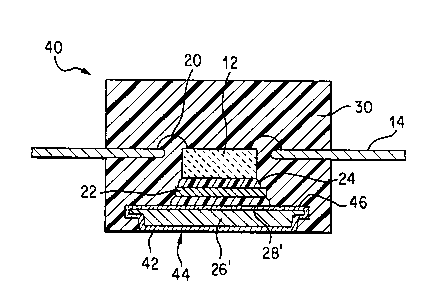
A molded plastic electronic package 40
representing a first embodiment of the invention is
illustrated in cross-sectional representation in ~igure
2. Those features of the molded plastic package 40
which perform substantially the same function as
structures illustrated in Figure 1 are identified by
like reference numerals. Those features of the molded
plastic package 40 which perform related functions in a
different manner are indicated by primed reference
numerals. An aluminum or aluminum alloy heat spreader
26' is, preferably, in thermal contact with a
semiconductor device 12. By thermal contact, it is
meant that the heat generated by the semiconductor
device 12 can travel a continuous path to an external
surface 4g of the aluminum or aluminum alloy heat
spreader 25'. The heat is not required to pass through
the molding resin 30.
The molding resin is a poor ther~al conductor.
Maintaining thermal contact between the device and heat
spreader, in accordance with the preferred embodiments
of the invention, impro-ves thermal dissipation. The
molding resin 30 should also only partially encapsulate
the heat spreader 26'. The exterior surface 44 of the
he~t spreader 26~ is, preferably, not encapsulated to
masimize thermal convection of heat generated by the
device to the surrounding environment. Although, a
fully encapsulated heat spreader is within the scope of
the invention.
W O 94/07263 PC~r/US93/08215
The semiconductor device 12 is bonded to a die
attach paddle 22 by means of a first bonding means 24.
The second bonding means 28~ joins the die attach paddle
22 to the aluminum or aluminum alloy heat spreader 26'.
The second bonding means 28' may be a low melting
temperature solder or polymer adhesive as known from the
prior art or a thermally conductive grease or B-stage
epoxy as described below.
The aluminum or aluminum alloy heat spreader 26'
is anodized. An anodization layer 42 improves both
corrosion resistance and adhesion to the molding resin
30. While the anodization layer may be any color or
transparent, black (shades of black through gray) is
preferred. Black radiates the most heat and is most
effective for dissipating heat from the package to the
surrounding environment. A black color also matches the
typical color of resin. As a result, the infrared
absorption characteristics of the package are not
affected by the heat spreader. Reflow soldering to a
printed circuit board is with the same temperature
profile as used with packages lacking the heat spreade..
The black color may be formed by the addition of
dyes or pigments, but the most durable color is formed
by integral color anodization. ~ollowing anodization,
the coating layer may be sealed to close the pores
inherent in anodization. One suita~le sealing process
is exposure to pressurized steam for 30-60 minutes. It
may be preferred not to seal the pores as mechanical
locking of the molding resin in the pores improves
adhesion as described below.
The aluminum alloys most suitable for black
integral color anodization are those designated by the
ASM (American Society for Metals) as 3xxx and 6xxx
series.
W094/07263 2 1 ~ ~ 8 8 1 PCT/US93~08215
--7--
Alloys of the 3xx~ series contain up to about 1.5
percent by weight manganese along with other alloying
elements. The alloys are characterized by good thermal
conductivity and about 20% higher strength than alloys
designated as lxxx series (having greater than 99.00%
aluminum).
Alloys of the 6~ series contain magnesium and
silicon in an approximate proportion to form Mg25i.
The alloys are characterized by good formability and
qood machinability. They are heat treatable and form a
precipitation hardened alloy.
A most preferred aluminum alloy is aluminum alloy
3003 which has a nominal composition of about 0.12
percent by weight copper, about 1.2 percent by weight
manganese and the balance aluminum. A black anodization
layer may be formed by integral color anodization in an
electrolyte containing a mixture of sulfuric and
sulfosalicylic acids in a concentration range of from
about 1-4 g/l H2SO4 and from about 50-120 g/l
C7H6O6S. The cell voltage is rapidly increased
such that the current density increases from zero to
over 7.53 A/dm (70 ASF~ within about 3 minutes. This
anodization process is described in more detail in U.S.
Patent No. 5,066,368 to Pasqualoni et al. The adhesion
of the molding resin to the anodized heat spreader is
further enhanced by mechanical locking. By proper
control of the anodization parameters, pores of a
desired size form in the anodization layer. A pore size
of from about 50 to about 500 angstroms provides
enhanced adhesion without weakening the strength of the
layer. A preferred pore size is from about 75 to about
200 angstroms.
The minimum thickness of the anodization layer 42
is that effective to prevent corrosion of the heat
WOg4/07~3 2 1 4 ~ ~1 PCT/U593/08~15 ~
spreader 26~. The anodization layer 42 should be as
thin as possible while retaining effectiveness because
the metal substrate is a better thermal conductor than
the anodization layer. A preferred thickness for the
anodization layer 42 is from about 0.0025mm to about
0.076mm (0.1-3 mils), with a preferred thickness being
from about 0.013mm to about 0.026mm (0.5-1.0 mils).
The advantages of the aluminum or aluminum alloy
heat spreader include a weight of about ~0% less than
that of a comparable copper or copper alloy heat
spreader. Surprisingly, as disclosed in U.S. patent No.
4,939,316 to Mahulikar et al., the thermal dissipation
of an electronic package with aluminum base components
is comparable to that of a similarly configured package
having copper base components. The reason for this is
believed to be that the limiting factor for the
dissipation of heat from the semiconductor device 12 to
the surface 44 of the heat spreader 26' is thermal
conduction through the first 24 and second 28' bonding
means. Packages having an aluminum or aluminum alloy
heat spreader are capable of removing approximately the
same amount of heat from the device as a comparable
package with a copper heat spreader.
~he anodization layer 42 provides ~he heat
spreader 26' with resistance to salt spray corrosion, as
well as resistance to other corrosives. A black color
provides better thermal conduction than a reflective
metallic surface such as a copper, aluminum or nickel.
Additionally, by varying the peak current density during
anodization, controlled diameter pores may be formed in
the surface of the anodization layer 42. These pores
provide improved mechanical locking to the molding resin
30.
~ W094/07263 2 1 ~ ~ ~ 8 1 . PCT/US93/08215
The improvement in adhesion when an aluminum heat
spreader is anodized as compared to a non-anodized
component is believed to be based on both a chemical
interaction with the molding resin and mechanical
locking. An anodized heat spreader has better adhesion
than one which is not anodized. A rough anodization
layer, achieved by varying the anodization parameters
(ie current or solution make-up) provides better
adhesion than a smooth anodized surface.
Another advantage of the anodization layer 42 is
electrical isolation. The anodized aluminum heat
spreader is electrically nonconductive. A semiconductor
device mounted on the heat spreader will not be at the
same voltage potential as the heat spreader and a
voltage pulse contacting the outside of the package will
not detrimentally affect the semiconductor device.
Further, when the outer lead ends are electrolytically
plated with solder, a typical operation following
package molding, the electrically nonconductive heat
spreader will not be coated with solder.
The adhesion of the heat spreader 26' to the
molding resin is further improved by mechanically
locking. As shown in Figure 2, the corners of the upper
surface 46 of the heat spreader 26' may extend beyond
the corners of the bottom surface 44 such that the
molding resin partially encapsulates the heat spreader.
It is desirable that the bottom surface 44 remain
exposed to the atmosphere to maximize the dissipation of
heat. Other configurations may also be employed to
mechanically lock the heat spreader in place in the
epoxy molding resin, such as protrusions, holes or edge
deformations.
The thermal dissipation of the molded plastic
package 40 may be further improved by using as the
W094/07263 2 1 ~ 4 8 8 1 ~ ` PCT/US93/08215 ~
--10--
second bonding means 28' a thermal yrease or B-stage
epoxy. The thermal grease 28~ is any suitable thermally
conductive grease such as a silicone grease. One
exemplary thermal grease is Omegatherm 24 manufactured
5 by Omega Engineering, Inc. of Stamford, CT.
When the thermal grease is utilized, the die
attach paddle 22 remains in thermal contact with the
heat spreader 26', but is not bonded to it. As a
result, the coefficient of thermal expansion mismatch
10 between the heat spreader 26' and the semiconductor
device 12 will not generate mechanical stresses on the
semiconductor device 12. Any stresses generated by the
coefficient of thermal e~pansion mismatch are
compensated by movement of the die attach paddle.
15 Thermal contact is maintained by corresponding movement
of the thermal qrease.
The advantages achieved through the thermal grease
are not limited to aluminum heat spreaders and improve
any electronic package having a coefficient of thermal
20 expansion mismatch the heat spreader and the
semiconductor device. The grease is particularly useful
for copper or copper alloy heat spreaders. To enhance
adhesion, the copper heat spreaders are preferably
coated with a second metal such as nickel as disclosed
25 in U.S. Patent No. 4,888,449.
Alternatively, the die attach paddle 22 may be
bonded to the aluminum or aluminum alloy heat spreader
26 by a thermally enhanced B-stage adhesive such as a
silver filled epoxy. The upper surface 46 of the heat
sink 26' is precoated with a layer Gf a conductive
adhesive 28' in form of a film or thin layer of liquid
and cured to the B-stage. By "B-stage" it is meant the
epoxy is partially cured. Adhesion to the die attach
paddle 26' occurs without completion of the cure
reaction.
W094/07263 2 1 ~ ~ 8 8 1 PCT/US93/08215
The heat sink 26' with the B-stage epozy 28'
laminated thereto is placed in a mold cavity. Ne~t, the
leadframe assembly which includes the semiconductor
device 12 and die attach paddle 22 is placed into the
mold. The leadframe assembly and the aluminum or
aluminum alloy heat spreader 26' except for the bottom
surface 44 are then encapsulated in molding resin 30
such as by injection molding. The molding resin is
heated to decrease viscosity during molding and the
heated resin either completes the cure or at least
partially cures the B-stage adhesive 28'. Complete
curing of the B-stage adhesive 28~, if required, occurs
during a post mold cure. One exemplary post mold cure
is to heat the molded package to about 175C in air for
several hours.
Preferred B-stage adhesives have a very low weight
loss (i.e. the adhesive has little out gassing) so that
air bubbles or voids do not form during the mold and
post cure. The B-stage adhesive should also be very low
stress, i.e., have a high degree of compliancy to
compensate for the coefficient of thermal e~pansion
mismatch between the aluminum or aluminum alloy heat
spreader 26' and the semiconductor device 12. A
preferred thickness for the B-stage adhesive is from
about ~.025mm to about 0.Slmm (0.001-0.020 inch), with a
preferred thickness of from about 0.0Slmm to about
0.25mm (0.002-0.010 inch).
The molded plastic package 50 illustrated in
cross-sectional representation in Figure 3, represents
ansther embodiment of the invention. In this
embodiment, the aluminum or aluminum alloy heat spreader
26' which preferably includes a black inte~ral color
anodization layer 42, is bonded to the leadframe 19 by a
third bonding means 52. The third bonding means 52 may
W 0 94/07263 ~ PC~r/US93/08215 -'
214 i881 -12-
be any suitable electrically insulating means such as a
polymer adhesive. A preferred third bonding means 52 is
an epoxy such as Abelstik 550 tAbelstik Laboratories,
Gardenia, California). Preferably, a cover 54 is bonded
to the opposite side of the leadframe 14 ~y a fourth
bonding means 56. The cover 54 may be fashioned from
any suitable material such as ceramic, plastic, glass or
metal. Most thermal dissipation is through the bottom
surface 49 of the heat spreader 26~ so the thermal
conduction characteristics of the cover 59 are not
critical. More importantly, the cover 54 should have a
coefficient of thermal expansion appro~imately matching
that of the heat spreader 26' to avoid flexure during
package heating or cooling. In the preferred
embodiment, the cover 54 is also formed from aluminum or
an aluminum alloy.
The fourth bonding means may be any electrically
insulating means such as a polymer adhesive. The
assembly is then encapsulated within a molding resin 30
with the bottom surface 44 of the heat spreader 26'
e~posed to the atmosphere to maximize thermal
dissipation. The advantage of this embodiment is that
the electrically active face 58 of the semiconductor
device 12 and the bond wires 20 do not contact the
molding resin 30. During package encapsulation, the
molding resin 30 is hot and traveling at high velocity.
Contact with the electrically active face 58 may abrade
the electrical circuits formed on that face or break
bond wires 20. After molding, the cured resin 30 has a
coefficient of thermal expansion different than that of
the semiconductor device 12. During temperature
fluctuations, there is movement of the semiconductor
device 12 relative to the molding resin 3C. The cover
54 creates a cavity 60 protecting the electrically
W094/07263 2 1 9 9 8 8 1 PCT/US93/08215
active face 58 of the semiconductor device 12, as well
as the bond wires 20 from contact with the molding resin
30.
While an uncoated aluminum or aluminum alloy heat
spreader may provide some of the advantages described
above, the full advantage of the invention is achieved
with an anodized aluminum heat spreader. A ~lack
integral color maximizes thermal conduction from the
exposed face of the heat spreader. The anodization
layer improves the adhesion between the heat spreader
and the molding epoxy as is apparent from the Example
which follows. The Example is intended to be
illustrative and not limiting.
EXAMPLE
A test apparatus 70 as illustrated in Figure 4 was
prepared by partially encapsulating two aluminum alloy
3003 strips 72 in a block of molding resin 30. The
strips 72 were pulled in opposing directions as
illustrated by reference arrows 74 with an Instron
tensile tester (Instron Corporation, Canton,
Massachusetts). Test strips 72 were evaluated as both
uncoated aluminum alloy 3003 and aluminum alloy 3003
with an integral color anodization layer. Other test
strips 72 were encapsulated in the resin ~lock and the
molded assembly placed in a pressure cooker at 121C and
100% relative humidity. Exposure time to the pressure
cooker was 96 hours. Table 1 indicates the force in
btoh MPa and psi reyuired to remove the test strips 72
from the block of molding resin 30.
W094/07263 2 1 4~ 1 PCT/US93/08215 ~i
-14-
TABLE l
~Test / Aluminum / Anodized Aluminum
/Condition / AlloY 3003 ~ Alloy 3003
/ / Mean Standard / Mean Standard
/ / MPa (psi~ Deviation / MPa (psi) Deviation i
/ / MPa psi / MPa psi /
/As cured / 4.59 665 l.37 l99 / 6.66 966 .41 60
/96 hours in/
/pressure
/cooker / 4.l0 594 l.29 187 / 5.78 838 .61 88
Table l shows the adhesion of the molding resin 30
to an anodized aluminum heat strip 72 is at least 45%
greater than the adhesion of the molding resin to an
unanodized aluminum test strip. A similar improvement
is observed after pressure cooker exposure.
An additional benefit is noted from the standard
deviations recorded on Table l. More consistent results
are achieved after anodization, indicating that the
uniform dispersion of surface pores created by integral
2Q color anodization presents more uniformity than achieved
by the random surface of unprocessed metal.
While the embodiments of the invention described
above include a single semiconductor device in thermal
contact with the aluminum or aluminum alloy heat
spreader, it is within the scope of the invention to
have a plurality of semiconductor device~ in thermal
contact with a single heat spreader. For example, U.S.
Patent No. 5,124,783 to Sawaya discloses a circuit
pattern mounted on a die attach paddle. A plurality of
semiconductor devices are bonded to the die attach
paddle and electrically interconnected to the circuit
pattern. The thermal dissipation of the disclosed
package would be greatly improved through the use of the
heat spreaders of the present invention, thereby
~ W094/07263 ~ , PCT/US93/08215
214'~i~38''1'
-~5-
permitting the use of higher power semiconductor devices
or a greater number or density of devices.
While the preferred embodiments of the invention
are drawn to an anodization layer on an aluminum or
aluminum alloy substrate, the beneficial effects of the
adhesion promoting coating may be applied to other
substrates as well. These other substrates include
aluminum based composites such as aluminum-silcon
carbide and aluminum based compounds such as aluminum
nitride.
While the preferred embodiment of the invention is
drawn to an anodization layer coating the aluminum or
aluminum alloy heat spreader, other coatings which
enhance adhesion are also believed to be beneficial.
These coatings include chromium, zinc, mi~tures of
chromium and zinc as well as mi~tures of chromium and
phosphorous.
One exemplary alternative coating is a
co-deposited layer of chromium and zinc. This coating
is known to improves the adhesion of a molding resin to
a copper or copper alloy substrate. The preferred
coatings as disclosed in U.S. Patent No. 5,098,796 have
a zinc to chromium ratio in excess of about 4 to l.
The co-deposited chromium zinc layer does not
provide electrical isolation as achieved by the
anodization layer. The co-deposited layer could be
deposited over the anodization layer to maintain
electrical isolation. Alternatively, if electrical
isolation is not necessary, the adhesion enhancing
coating may be applied to any heat spreader.
It is apparent that there has been provided in
accordance with this invention an anodized aluminum heat
spreader which fully satisfies the objects, means and
advantages set forth herein before. While the invention
W O 94/07263 2 1 4 4 8 8 1~ PC~r/US93/0821~ - '
-16-
has been described in combination with specific
embodiments thereof, it is evident that many `
alternatives, modifications and variations would be
those apparent to those skilled in the art in light of
the foregoing description. Accordingly, it is intended
to embrace all such alternatives, modifications and
variations as fall within the spirit and broad scope of
the appended claims.