Note: Descriptions are shown in the official language in which they were submitted.
2145 4'~ 1
57,976
OVERCURRENT TRIP UNIT WITH SEPARATELY
ADJUSTABLE NEUTRAL PROTECTION
BACKGROUND OF THE INVENTION
Field of the Invention
This invention relates to overcurrent trip units for circuit breakers, and
more particularly to such trip units providing protection for the neutral
conductor
which is adjustable separately of the line protection functions.
Background Information
In three-phase electric power systems servicing normal, balanced loads,
no current, or minimal current, flows in the neutral conductor. However, in
installations where single phase loads draw current from a three-phase supply,
substantial currents can be generated in the neutral conductor which can cause
overheating. Such neutral conductor overheating can be caused by inexpensive
power supplies used in some computers. Such loads can generate a third
harmonic on the neutral conductor having an amplitude which is the square root
of 3 times the line current. In new installations, the neutral conductor can
be
sized to accommodate such neutral currents. However, in many older
installations in which the wiring is no longer easily accessible, the neutral
conductor may typically be one-half the size of the phase conductors.
In the United States, codes do not permit opening the neutral conductor.
However, interruption of current in all of the phase conductors terminates
neutral current. While separable contacts are not provided in the neutral
conductor, some circuit breakers monitor neutral current and trip upon
detection
of selected neutral overcurrent conditions. Typically, the sensed neutral
current
is auctioneered along with the phase currents with desired scaling of neutral
current relative to the phase currents being fixed by selection of the per
unit
value of the current transformer sensing neutral current relative to the per
unit
values of the current transformers sensing phase current. Such fixed scaling
is
set at the factory and is not easily changed.
CA 02145471 2000-06-02
- 2 - 57, 976
There is a need for a circuit breaker trip unit with neutral protection which
is operator adjustable separate from the phase protection. This would allow a
single model of a circuit breaker to be easily adapted in the field to be
used, for
instance, with an installation in which the neutral conductor is one/half the
size
of the phase conductors, or an installation in which the neutral conductor is
twice the size of the phase conductor. Preferably, this separately adjustable
neutral protection would include long delay trips, short delay trips and
instantaneous trips.
SUMMARY OF THE INVENTION
These needs and others are satisfied by the invention which is directed
to a circuit breaker trip unit providing neutral protection which is operator
adjustable separately from the phase protection. In the preferred embodiment
~ 5 of the invention, this separate neutral protection is selectable as a
percentage,
which may be greater or less than 100%, of the phase protection. More
particularly, the pick-up currents for the long delay, short delay and
instantaneous protection for the neutral conductor are selected as a
percentage
of the long delay, short delay and instantaneous pick-up currents for the
phase
currents. In a circuit breaker where the pick-up currents for the phase
protection functions are adjustable as a first factor times the rated current
for
the circuit breaker, the pick-up currents for the neutral protection functions
are
selected as a second factor times the rated current. The time intervals for
the
long and the short delays for phase protection are used for the neutral
protection. In the exemplary embodiment of the invention, the neural current
is
scaled by the ratio of the first factor to the second factor and then
auctioneered
with the phase currents, with the protection algorithms only run on the
largest of
the aucioneered currents.
As another aspect of the invention, a neutral overload alarm is actuated
when a high load threshold level, which is less than the pick-up current for
the
neutral long delay protection, is exceeded.
~14547I
- 3 - 57, 976
BRIEF DESCRIPTION OF THE DRAWINGS
A full understanding of the invention can be gained from the following
description of the preferred embodiments when read in conjunction with the
accompanying drawings in which:
Figure 1 is a schematic circuit diagram, partially in block diagram form of
a circuit interrupter incorporating the invention.
Figure 2 is a graphical representation of the current-time characteristic of
the circuit breaker of Figure 1 in accordance with the invention.
Figures 3A - 3F, when arranged as shown in the diagram of Figure 3,
form a schematic circuit diagram of the trip unit which forms part of the
circuit
breaker of Figure 1.
Figure 4 is an illustration of an operator's panel which form part of the
trip unit of Figures 3A - 3F.
Figure 5 is a flow chart of a suitable computer program utilized by the trip
unit of Figures 3A - 3F to implement the invention.
Figure 6 is a flow chart of a subroutine used by the computer program
charted in Figure 5.
DESCRIPTION OF THE PREFERRED EMBODIMENTS
Figure 1 illustrates a circuit breaker 1 in accordance with the invention
connected to provide protection for a three-phase/four-wire electrical system
3.
This electrical system has three-phase conductors 5A, 5B, and 5C and a neutral
conductor 5N. The circuit breaker 1 has three primary current transformers 7A,
7B, and 7C for sensing current flowing in the respective phase conductors.
These primary CT's are physically located inside the housing 9 of the circuit
breaker 1. A fourth primary current transformer 7N, external to the circuit
breaker 1, monitors current flowing in the neutral conductor 5N. The primary
CT's 7 are selected so that the full scale rated current of the electrical
system
generates on the secondary a 5 ampere signal, for instance. All of the phase
- 4 - 57, 976
primary CT's, 7A - C, are the same size; however, the neutral primary CT 7N
can be a different size depending upon the relative size of the neutral
conductor
5N to the size of the phase conductors 5A-C. The auxiliary current
transformers 11 A, B, C, N step down the full scale rated current to, for
example, 0.1 amperes. The secondaries of the primary phase CT's are
connected at 13.
The two wire outputs of the secondary windings of the current
transformers 11 A, B, C, N are applied as inputs to a digital trip unit 15.
The
digital trip unit 15 which is described in Figures 3A-3F performs protection
functions based on the monitored phase and neutral currents. These protection
functions include generating trip signals which actuate a flux shunt trip
device
17 to open separable contacts 19A, 19B, and 19C in the phase conductors 5A -
C. Where applicable codes permit, a set of contacts (not shown) can also be
included in the neutral conductor 5N if desired.
The circuit breaker 1 can also include a relay 21 which may be used for
generating a neutral alarm in accordance with the invention. The relay 21 is
actuated by a signal on the lead 23 from the digital trip unit 15. The relay
21
closes a set of contacts 25 which provides a contact closure indication at
output terminals 27. These terminals 27 may be connected to a remote
indicator (not shown). The neutral alarm is generated when current in the
neutral conductor exceeds a high load threshold.
Figure 2 is a logarithmic plot of an exemplary current-time protection
characteristic of the circuit breaker 1 in accordance with the invention.
Current
is plotted on the abscissa and time on the ordinate. The right hand curve 29
is
the phase protection curve and the left hand curve 31 is the neutral
protection
curve. The farthest right vertical portion 33 of the phase curve 29
establishes
the instantaneous trip current for the phase conductors. This instantaneous
trip
function provides protection against short circuits in the phase conductors.
Typically, the circuit breaker 1 would be used in an electrical system with
other
circuit breakers. The short delay trip function allows coordination with other
circuit breakers in the system, as is well known. The short delay trip is
~I45471
- 5 - 57, 976
generated if current exceeds a pick-up value determined by the vertical
section
35 of the curve 29 for an interval determined by the horizontal line 37.
The circuit breaker 1 also provides long delay protection. The long delay
function provides protection from overheating of the conductors of the
electrical
system due to persistent excessive current. Typically, long delay protection
is
selected so that a trip is initiated if a current which is six times a long
delay
pick-up current level persists for a selected period of time. The long delay
pick-
up current value is represented by the vertical line segment 39 in Figure 2.
The
selected time for the long delay trip is indicated by the time value at the
point
41. As the purpose of the long delay trip is to protect against overheating of
the electrical system, an /~t function which approximates the thermal
condition
of the electrical system is commonly used for long delay protection and is
represented by the diagonal portion 43 of the curve 29. It can be appreciated
from Figure 2 that a current which exceeds the long delay pick-up value will
result in an earlier long delay trip and is represented by the time value
derived
from the diagonal portion 43 of the curve 29 corresponding to the higher
current. In some installations, an /~t function is also used for a short delay
and
is represented by the diagonal dotted line segment 45 in Figure 2. In the
example shown in Figure 2, the short delay protection overlaps the long delay
protection as indicated by the vertical line segment 35 intersecting the
diagonal
line segment 43 above and to the left of the point 41. As will be seen later,
in
the explanary circuit breaker separate switches are provided for setting the
phase instantaneous pick-up current and the phase long delay pick-up. A
separate switch is also provided for setting the phase short delay pick-up
current; however, it is set as a factor times the long delay pick-up current
and
is therefore dependent thereon. This dependence is indicated by the stripped
portion of the curve 29.
In accordance with the invention, separate operator setable protection is
provided for the neutral conductor. In the preferred embodiment of the
invention, instantaneous, short delay and long delay protection are provided
for
the neutral conductor. In the exemplary embodiment of the invention, the pick-
CA 02145471 2000-06-02
- 6 - 57, 976
up values of current for the instantaneous, short delay and long delay neutral
protection are scaled to the pick-up values for phase protection. Furthermore,
in the exemplary trip unit 15 the time delays for short delay and long delay
for
phase protection are also used for neutral protection. Therefore, the curve 31
representing the protection characteristic for the neutral conductor is merely
shifted horizontally by an amount related to the scaling factor. The dotted
curve 31' shows that the neutral protection curve can be shifted to the right
of
the phase protection curve, as where the neutral conductor is larger than the
phase conductors. As the reason for providing separate operator selectable
neutral protection is to accommodate for the fact that the size of the neutral
conductor can vary relative to the size of the phase conductors, providing for
a single adjustment which scales the neutral protection to that of the phase
protection is desirable. Typically, the same factors which dictate the
selection
of the time interval and the pick-up values for the phase conductors will be
applicable to the neutral conductor, and this single adjustment allows a
simple
correction for the relative size of the neutral conductor. It is to be
understood,
however, that separate times and different relative pick-up values for
instantaneous, short delay and long delay pick-ups could be used for the
neutral
protection.
Figures 3A - 3F when aligned as illustrated in Figure 3 illustrate a
schematic circuit diagram of the digital trip unit 15 of the circuit breaker
1. The
heart of the digital trip unit is an integrated circuit (IC) chip 47. This
custom
chip is a complementary metal oxide semiconductor (CMOS) IC which includes
an on-board microprocessor, an analog-to-digital (A/D) subsystem and various
input/output devices on a single monolithic chip. The details of this chip are
disclosed in U.S. patent number 5,270,898 issued on December 14, 1993.
The IC described in this patent includes circuitry for communication through
leads 48 protected by surge protection circuits 50 between the circuit breaker
and remote devices (not shown) for remote control and monitoring. While such
communications are compatible with the present invention they are not a
necessary part of a circuit
~I45471
_ _
- 7 - 57,976
breaker in accordance with the invention, and hence will not be discussed
herein.
The digital trip unit 15 includes an extender board 49 which plugs into
the housing of the circuit breaker for inputting and outputting signals to the
digital trip unit. The extender board 49 includes pairs of connections 51 A,
B,
C, N for inputting phase currents and neutral currents from the secondary CT's
1 1 A, B, C, N, respectively. These phase and neutral current signals are
converted to do signals by full wave rectifiers 53A, B, C, N. The do outputs
of
the full wave rectifier bridges 53 are applied to a common lead 55 which
supplies current to a power supply 57. The power supply 57 provides a roughly
regulated voltage for powering the digital trip unit 15. Thus, the digital
trip unit
is energized by the currents in the protected electrical system. Additional
circuits 59 connected to the IC 47 provide a reference voltage and 5 volt
regulated supply for use by the IC and other circuits in the digital trip unit
15.
The do currents produced by the full wave rectifiers 53A, B, C, N are
applied to current sensing resistors 61 A, B, C, N, respectively. The sensed
currents are read into the IC chip 47 through input resistors 63A, B, C, N. As
explained in the referenced patent, these currents are converted to voltages
by
the analog circuits in the IC 47 and digitized by the on-board A/D converter
for
input to the microprocessor.
The analog do currents from the full wave rectifier bridges 53 are also
auctioneered through the diodes 65A, B, C, N. If the largest analog current
exceeds a value determined by the zener diode 67 to which these diodes are
connected by a lead 66, an override trip signal is generated at the output
terminals 68. This override signal trips the circuit breaker instantaneously
to
avoid the delays that are inherent in the digital circuitry in detecting and
responding to overcurrent conditions. It only responds to very large _
overcurrents such as would be caused by a bolted short circuit. The override
trip is reported to the microprocessor through the lead 69.
~1~5471
- 8 - 57, 976
The phase A ac current is also applied to the IC 47 as the signal SIGNIA
over lead 71 to provide an indication of the sign of the current and is used
by
the microprocessor in determining the frequency of the currents in the
protected
system.
The microprocessor incorporated in the IC 47 uses the current signals
representative of the phase and neutral currents to provide instantaneous,
short
delay and long delay protection in accordance with the protection curves
discussed in connection with Figure 2. As mentioned, the protection for the
neutral conductor is separately adjustable from the phase protection in a
manner
to be discussed below.
When the overcurrent-time limits are exceeded, the microprocessor on the
IC generates a TRIP signal on lead 73. This trip signal turns on a FET 75
which
provides a ground for discharge through a lead 76 of a capacitor 77 in the
power supply 57 to actuate the flux shunt trip device 17 connected to the
connection 79 on the extender board 49 which in turn opens.the contacts 19.
A fly back diode 78 is provided across the shunt trip device. The
microprocessor also generates signals INST, SHORT, NEUTRAL, and LONG on
leads 81, 83, 85 and 87, respectively. These signals are latched by a latch 89
for energization of INST, SHORT, and LONG, LEDs 91, 93, 95 and 97 which
provide a visual indication of the cause of trip. If the trip was caused by an
overcurrent in one of the phase conductors, one of the LEDs 91, 93, or 97 will
be energized. If the overcurrent occurred in the neutral conductor, the
neutral
LED 95 will be energized as well as one of the LD, SD or INST LEDs to indicate
the type of neutral trip.
The microprocessor also generates alarm signals which provide notice of
a condition which could lead to a trip. Thus, an LDALARM signal is generated
on the lead 99 if the circuit breaker has tripped on a long delay. This signal
is
provided at a connection 101 on the extender board 49 for turning on an
indicator on the front panel of the circuit breaker, and a remote alarm if
desired.
The microprocessor generates a HLALARM signal on a lead 103 when a current
reaches a percentage, for instance 85%, of the pick-up value for a long delay
CA 02145471 2000-06-02
- 9 - 57, 976
trip. This signal is provided to the HILOAD ALARM connection 105 on the
extender board 49. The microprocessor also generates an SCALARM signal on
a lead 107 as a short circuit alarm indicating that an instantaneous trip has
been
generated. This signal is provided to the SHCK ALRM connection 109 on the
extender board. A NEUTRAL ALARM signal is generated on the lead 1 10 when
an operator selectable neutral current high threshold level, which is less
than the
pick-up current for neutral long delay protection is exceeded. Alternatively,
the
neutral alarm can be generated when any of the neutral protection pick-up
values are exceeded. This signal is available at the output on the extender
board. The zener diodes 118 protect the IC 47 from any surges from circuits
connected to the alarm outputs.
The digital trip unit 15 also can provide zone interlocking as is known in
the art. Zone interlocking is provided in connection with the short delay
protection in order to coordinate tripping of upstream and down stream circuit
breakers in a manner which is well known. The short delay zone interlock out
signal is provided by the microprocessor on lead 111 connected to the extender
board 49 at the SOUT X connection 113. The short delay zone interlock input
signal is input on lead 1 15 to the microprocessor from the SINX connection 1
17
on the extender board 49.
The digital trip unit 15 can be used with various frame sizes of circuit
breakers. In addition, each of the frame sizes of circuit breakers with which
the
digital trip unit 15 is compatible can be used to protect an electrical system
3
in which the maximum continuous current permitted is less than or equal to the
maximum continuous current permitted by the frame. In order to provide this
information to the digital trip unit 15, a suitable, removable rating plug 1
19 can
be plugged into the digital trip unit. The rating plug 1 19 contains a number
of
resistors (not shown) which are keyed to the frame size, and which set the
maximum or rated current for the particular installation. This rated current
can
be the maximum current allowed by the frame size or some smaller value. For
instance, if the maximum current allowed by the frame is 2,000 amperes, the
resistor combination in the plug 119 can be selected to indicate to the
CA 02145471 2000-06-02
- 10 - 57,976
microprocessor that the rated current is 2,000 amperes, 1, 500 amperes, 1, 200
amperes, or any other value less than 2,000 amperes. The microprocessor
reads the FRAME setting through a dedicated input MUXS and the MXO input
of the multiplexor on the IC 47 and reads the rated current through the MXO
and dedicated input MUX6.
The rating plug 119 also contains a battery (not shown) which provides
a 5 volt source of power + E. As indicated previously, the digital trip unit
15
is powered by current from the protected circuit. When the circuit breaker
trips
and the current is interrupted, the power to the microprocessor is also
interrupted. The five volt do power + E provided by the battery on the rating
plug 119 is applied to the latch 89 so that the cause of trip LEDs 91, 93, 95,
and 97 remain energized following a trip. This battery is also used to
provide,
through the connection + E, power for a reset button 121 which generates a
TRIP reset signal for the microprocessor on lead 123.
When the power to the microprocessor is lost upon tripping of the circuit
breaker, the calculation of the thermal state of the load represented by the
lZt
characteristic maintained by the long delay trip function is also lost. As is
known in the art, the voltage representative of the thermal excitation state
of
the load, as represented by the /~t value, is stored on an external capacitor
125.
In the exemplary digital trip unit 15, the capacitor 125 continuously tracks
the
thermal excitation state signal generated by the microprocessor. When the
circuit breaker trips, and the microprocessor becomes unpowered, the capacitor
125 discharges through a resistor 127. The value of resistor 127 is selected
so that the voltage on the capacitor 125 discharges at a rate which mimics
cooling of the load. When the microprocessor becomes repowered, it utilizes
the residual voltage on the capacitor 125 to set an initial value for the
continued
calculation of the thermal excitation state of the load.
A status LED 129 is energized intermittently by the microprocessor to
provide a status indication that the microprocessor is operational. The
digital
trip unit 15 can be tested by momentarily depressing a test button 131. This
provides a TEST input to the microprocessor on lead 123.
~~~54'~i
- 11 - 57,976
The settings for the various protection functions are input to the
microprocessor through a data bus 135. Connected to the data bus is a first
set of operator adjustable switches 137 for adjusting the parameters for phase
protection, a second set of switches 139 for setting neutral protection, and a
switch 141 for setting the test parameters. The first set of switches 137 for
setting phase protection includes: a switch 143 for setting the long delay
pick
up level for phase protection, a switch 145 for setting the long delay time, a
switch 147 for setting the short delay pick-up level for phase protection, a
switch 149 for setting the short delay time, and a switch 151 for setting the
instantaneous pick-up level.
The second set of switches 139 includes a switch 153 for setting the
long delay pick-up level for neutral protection, and switch 155 for setting
the
threshold level for the neutral high load alarm. Each of the switches 141-155
has eight selectable settings. The settings of the switches 141-155 are read
by the IC 47 through the data bus 135. The IC ports PBO-PB7 determine which
switch is to be read. The port connected to the switch to be read is set to
ground so that the wiper of that switch is grounded. The ports connected to
the remaining switches are set to a high impedance so that the wipers of those
switches are pulled up to + 5 volts by the associated pull-up resistor 136.
The
ports PD1-PD7 read in the wiper position of the interrogated switch in
parallel.
The terminal engaged by the wiper will be at ground. All of the remaining
terminals on the interrogated switch are pulled-up to + 5 volts by the
associated
resistors 138.
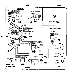
Figure 4 illustrates the operator panel 157 for the digital trip unit 15. The
operator's panel 157 includes a graphical representation 159 of the phase
current-time characteristic and a representation of the neutral current-time
characteristic 161. The switches 143, 147 and 151 for setting the phase long
delay, short delay and instantaneous pick-up values, respectively, are mounted
on the operator's panel adjacent the associated portion of the phase current-
time characteristic 159. The switch 145 for setting the long delay time, and
the
switch 149 for setting the short delay time are also located appropriately
next
CA 02145471 2000-06-02
- 12 - 57,976
to the phase curve 159. The long delay pick-up setting is displayed in a
window 163 next to the switch 143 and adjacent to the window is a legend
indicating that it displays the phase long delay setting. It also indicates
that the
long delay setting /, is equal to the setting in the window multiplied by /"
which
is the rated current set by the rating plug. This factor which sets the long
delay
pick-up level can only be a fraction. Similarly, a window 165 displays the
short
delay pick-up setting which is a multiple of the long delay pick-up value /,.
Thus, when the long delay pick-up setting is adjusted, the short delay pick-up
level is adjusted with it. This feature is disclosed in commonly owned U.S.
patent number 5,367,427 issued on November 22, 1994. A distinguishing color
167 is used on this portion of the curve 159 to indicate this dependency. The
instantaneous trip pick-up setting is displayed in a window 169 adjacent to
switch 151. As indicated, the instantaneous pick-up level is a multiple of the
rated current, In, set by the rating plug 119. The long delay time setting is
~ 5 displayed in the window 171 while the short delay time is displayed in the
window 173. The legend next to the long delay time window 171 indicates that
the circuit breaker will trip after the displayed time in seconds with the
phase
current at six times the long delay pick-up level I',. as discussed
previously. The
INST, SHORT and LONG LEDs, 91, 93 and 97 are mounted in the operator's
20 panel at the appropriate location in the graphical representation 159 of
the
phase protection curve.
The switch 153 for setting the neutral long delay pick-up value is similarly
located adjacent to the upper portion of the graphic representation 161 of the
neutral protection curve on the operator's panel 157. Just above the switch
25 153 is the neutral setting window 175 in which the neutral long delay pick-
up
setting is displayed. While this switch is labeled "neutral long delay
setting",
it is really a neutral conversion factor that affects all the neutral
settings,
including instantaneous. An example of values for the neutral long delay
setting
would be eight values from .25 to 2.0 in increments of .25. As indicated by
the
30 legend on the operator's panel, the neutral long delay pick-up value /, is
equal
to the selected factor times /" , the rated current set by the rating plug 1 1
9.
2145471
- 13 - 57, 976
The switch 155 for establishing the neutral high load alarm setting is also
placed on the operator's panel, adjacent the representation 161 of the neutral
protection curve. The settings of the neutral high load alarm are displayed in
the window 177 directly above the switch 155. In addition, the neutral LED 95
which will be illuminated in response to a neutral trip and which flashes in
response to a high load alarm is also located next to the neutral protection
curve
161.
The test switch 141 which sets the pick-up value for testing is also
displayed in the lower right hand corner of the operator's panel 157.
Immediately above the switch 141 is a window 179 displaying the test pick-up
setting. The adjacent legend recites the conditions for test trip. Below the
test
set switch 141 are the test button 131 the reset switch 121 and the status LED
129. The rating plug 119 is mounted in the upper right hand corner of the
operator's panel 157.
Figure 5 illustrates the flow chart of the interrupt protection routine
implemented by the microprocessor on the IC 47. This interrupt protection
routine 179 is called at 181 approximately every 4 milliseconds, or four times
per cycle. Upon being called, the routine first sets the timer at 183 to
implement the next interrupt, and then services the ATR relays such as the
neutral alarm relay 21 at 185. Each time four samples have been completed,
as determined at 187, the instantaneous and short delay protection
calculations
are made at 189. After each 64 samples, as determined at 191, long delay
protection is calculated at 193. Every 256 samples, as determined at 195,
other related routines such as calculation of energy and power are implemented
at 197. In each case, the routine returns at 199 to the calling routine.
Figure 6 illustrates a subroutine used by the routine 179 for integrating
the phase and neutral protection. The samples accumulated for each of the
phase currents and neutral current are processed to generate RMS current
values as is known. The neutral current is then scaled at 201. For long and
short delay protection, this scaling is implemented by multiplying the neutral
current by the ratio of the phase long delay pick-up setting to the neutral
long
_2145471
- 14 - 57, 976
delay pick-up setting. Since phase instantaneous protection is a function of
the
rated current /" and not /,, the neutral current is multiplied by 1 over the
neutral
long delay setting to scale it for auctioneering with the phase currents for
instantaneous protection. The scaled RMS neutral current is then auctioneered
with the phase RMS currents at 203 with the current of highest amplitude, ImBX
being supplied to the phase protection algorithms at 189, 193 and 197 in
Figure
5.
The present invention allows a circuit breaker to be used in installations
with varying sizes of neutral conductors through operator selection of a
neutral
protection scaling factor on the front face of the trip unit. This is a useful
feature for many installations such as where the use of many personal
computers and other electronic equipment with single phase power supplies
which increase the currents on the neutral conductor have increased the need
to provide adequate neutral protection.
While specific embodiments of the invention have been described in
detail, it will be appreciated by those skilled in the art that various
modifications
and alternatives to those details could be developed in light of the overall
teachings of the disclosure. Accordingly, the particular arrangements
disclosed
are meant to be illustrative only and not limiting as to the scope of
invention
which is to be given the full breadth of the claims appended and any and all
equivalents thereof.