Note: Descriptions are shown in the official language in which they were submitted.
2 1 ~ ~ 7 8 ~
:" '
DC RESISTANCE WELDING APPARATUS
This application is a divisional of Application Ser.
No. 2,003,245, filed November 17, 1989.
The present invention relatas to a DC resistance . -
welding apparatus for resistance-welding workpieces with a
direct current, and more particularly to an inverter-type DC
resistance welding apparatus for rectifying three-phase AC
electric energy into DC electric energy, converting the DC
10 electric energy to high-frequency AC electric energy, then -
converting the high-frequency AC electric energy again into DC
electric energy with a welding transformer and rectifiers, and
then supplying the DC electric energy to welding electrodes to
weld workpieces.
Resistance welding apparatus include a pair of
electrodes for gripping a set of workpiece therebetween.
While a welding current is being supplied between the
electrodes to generate Joule heat, the electrodes are pressed ;
against the workpieces to weld the workpieces to each other.
The resistance welding is highly efficient as it requires no
welding rods.
The resistance welding process requires an electric
current much greater than other welding processes such as the
arc welding process. Therefore, the welding transformer used
by the resistance welding process is large and heavy. The
large and heavy welding transformer is one of the drawbacks
which make it difficult to install the resistance welding '
apparatus on the arm of a welding robot or the like. ~ ~
'i ,-, ,', .
1 , ~ I ~ ,' ~ , ' ;.,:
-- 1 --
2~4 :37~
. ~ .
To make the welding transformer srnaller in size, ~ :
there has recently been employed an inverter-type DC resis~
tance welding apparatus which converts DC electrlc energy to ..
high-frequency AC electric energy, supplies the high-
frequency AC electrlc energy to a welcling transformer to
lower the voltage thereof, then converts the high-frequency
AC electric energy to DC electric energy, and supplies the
DC electric energy to welding gun arms. The DC electric .~
energy is first converted to the high-frequency AC electric ~.
energy because the high-frequency AC electric energy allows .'~
the welding transformer to be relatively small and light-
weight since the cross-sectional area of the core of the
. ~ ........
welding transformer is inversely proportional to the fre- '~
quency of the hlgh-frequency AC electric energy. The reason .;. '~":
for converting the high-frequency AC electric energy back to . . :;
the DC electric energy for application to the welding gun
arms ls that the DC electric energy supplied to the welding
gun arms avoids a voltage drop which would otherwise be ... .
.-
caused by an increased high-frequency impedance due to the
stray inductance resulting from the length and shape o~ the . m;.
welding gun arms, and also avoids a voltage drop which would
otherwise be developed by the skin effect of the welding gun
! ~i arms,'iso that the welding apparatus is highly efficient ih ;
~ operation. .~:.
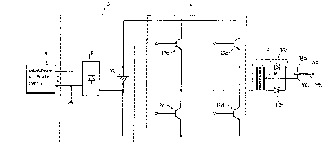
one inverter-type DC resistance welding apparatus
ls shown in FIG. 1 of the accompanying drawings. The DC .
;'' '''~'.'.'~'.'.',',''
,~ . .~..,
- 2 -
2 ~
resistance welding apparatus comprises a converter unit 2, an
inverter unit 4, and a welding transformer assembly 6
including a welding transformer 14. Three-phase AC electric
energy from a commercial three-phase AC power supply 7 is
converted to DC electric energy by a rectifier 8 and a
capacitor 10 of the converter unit 2, and the DC electric ;-
energy is then converted to AC electric energy having a fre-
quency higher than that of the three-phase AC electric
energy by the inverter unit 4 which comprises a bridge of
transistors 12a through 12d. The high-frequency AC electric
energy is then converted to DC electric energy again by the
welding transformer 14 with a central tap 19 on its secon~
dary winding and rectifiers 16a, 16b. The DC electric ~
energy is then supplied between welding electrodes 18a, 18b. ;
The welding electrode 18a is connected to the common joint ;;
between the rectifiers 16a, 16b, and the welding electrode ~
18b is connected to the central tap 19. A pair of work- ~;
pieces Wa, Wb to be welded togethèr is placed between the
welding electrodes 18a, 18b. When a welding current is
passed between the welding electrodes 18a, 18b through the
workpieces Wa, Wb, the contacting surfaces of the workpieces
Wa, Wb are melted and welded to each other.
i I DC resistance welding apparatus are always required
to supply a large welding current and to be small in size.
A large welding current is preferable when welding steel
sheets such as plated steel sheets containing materials of
- 3 - '~
,~ ~,,,,., ., .,",,,, ., .,,,.i " " , - " ~ , ",~ , ," .,, ", ~ .
,,.,;,.,.,, ,~.,,.. ,,, : ~
5~0
different melting points or welding aluminum sheets or the
like having a large thermal conductivity.
If the current capacity of the conventional DC
resistance welding apparatus is to be increased and the DC
reslstance welding apparatus is to be installed on the arm ~
of a welding robot, then the welding transformer 1~ will be ~ -
of an increased weight, requiring the robot to be large in ';-~
size, and it is required to connect the transistors 12a ~;
through 12d of the inverter unit 4 or the rectifiers 16a,
16b parallel to each other. AS a result, the DC resistance ' -
weld1ng apparatus may have stability and reliability ';
problems. '~'
Heretofore, the transistors of the inverter are ~.
operated within a continuous DC rating range. The inverter
is designed such that even if driver circuits connected to
the bases of the kransistors malfunction and the transistors
remain conductlve, the inverter wlll not be broken insofar '~
as it is within its thermal limits. The actual operating
range of the inverter is therefore required to be smaller
than the continuous DC rating range. As a consequence, the
conventional DC resistance welding apparatus is not suitable
for use in applications in which a large welding current is
to be supplied to the welding electrodes. ~ }
SUMMARY OF THE INVENTION ''~
It is a general object of the present invention to '~
provide a DC resistance welding apparatus which has a plu-
- 4 ~
. .
'-' 21~37~D
: !
rality of parallel-connected rectifying circuits each com-
prislng a welding transformer and rectifiers, so that a
large welding current can be supplied to workpieces, and
which is small in size and light in weight.
Another object of the present invention is to pro-
vide a DC resistance welding apparatus having a means for
monitoring the time in which semiconductor devices such as
transistors of an inverter unit are conducted, to allow the - -
semiconductor devices to be operated with a current larger
than a continuous rating range, so that a large welding cur-
rent can be supplied to workpieces. ';
Still another object of the present invention is to
provide a DC resistance welding apparatus having means for
individually detecting failures of parallel inverters, such
as output reductions or overcurrents thereof, so that all
the inverters can quickly be inactivated in response to
detection of such a fallure.
Yet another ob~ect of the present invention is to
provide a DC resistance welding apparatus in which the
trailing edges of switching signals are equalized in tlming
depending on the distorting action of welding transformers
connected to parallel inverters, for thereby preventing ove-
rcurrents from belng generated at the trailing edges of inv-
erter outputs for increased efficiency.
Yet still another object of the present invention ~ '~
is to provide a DC resistance welding apparatus in which a
-
- 5 ~
''" " '
21~ ~ 7 8 ~
si~nal corresponding to an energized conidi-tion of workpieces
to be welded can indirectly and accurately be produced from
a change in a current upon switching operation of inverters,
and the application of electric energy to the workpieces ls
stopped based on the signal thus produced, so that the work~
~- . .. ;.:
pieces can appropriately be welded. ~;~. .:
A further ob~ect of the present lnvention is to
provide a DC resistance welding apparatus comprising a pair ~.
of welding electrodes for sandwiching workpieces to be ;;~
welded therebetween, and a circuit connected to the welding J
electrodes for supplying a welding current to the weldlng '.~
electrodes, the circuit comprising a plurality of parallèl- .'
connected rectifying circuits each comprising a welding i;.
transformer and rectifying means.
A still further ob;ect of the present invention is .. ;~'
to provide the DC resistance welding apparatus wherein the
welding transformer includes a secondary winding having a ~. ~';?';
central tap, and the rectifying means comprises a pair of
rectifiers, the central tap serving as one output terminal
of each of the rectifying circuits, the secondary winding .
havin~ one end connected to one terminal of one of the
rectifiers, and the other end connected to one terminal of
the other of the rectifiers, the other terminals of the rec~
tif~ers being connected to each other as another output ter- ~. '
minal of each of the rectifying circuits, the one output
terminals of the rectifying circuits being connected
~. .~ ,,j.....
- 6
~", ~;
~ 1 4 ~) 7 ~
.. . -
together to one of the welding electrodes, and the other
output terminals of the rectifylng circuits being connected
together to the other of the welding electrodes.
A yet further ob~ect of the present invention is to
provide the resistance welding apparatus further including
an inverter unit comprising a plurality of inverters con-
nected respectively to the rectifying circuits for driving
the rectifying circuits. :~
A yet still further object of the present invention
is to provide the DC resistance welding apparatus further
including main control means connected to the inverters, and
current detecting means for generating a signal proportional
to the welding current supplied from the circuit to the .;~
welding electrodes and feeding the signal back to the main '~
control means, the main control means having feedback con- ~
trol means for keeping the welding current constant based on ~;; '.
the signal fed from the current detecting means to the main
control means. ~ -
Another ob~ect of the present invention is to pro- :
vide the resistance welding apparatus further including aux- ~:
iliary control means connected respectively to the
inverters, and current detecting means for generating sig-
nals proportional to branch welding currents supplied I ~ .
respectively from the rectifying circuits and feeding the :~
signals back to the auxiliary control means, the auxiliary ..
control means having feedback control means for keeping the
,
- 7 ~
i . , . , , , , ~:, : ,,,.. ~ . . -
i~ 2 ~ ~ ~ 7 ~
branch welding currents constant based on the signals Eed
from the current detecting means to the auxiliary control
means.
Still another ob~ect of the present invention is to ':~
provide the DC resistance welding apparatus further includ~
ing auxlliary control means connected respectively to the - -
inverters, first current detecting means for generating sig~
nals proportional to branch welding currents supplied ;
respectively from the rectifying circuits and feeding the .'~
signals back to the auxiliary control means, the auxiliary .';
control means having feedback control means for keeping the '.. ~;~
branch welding currents constant based on the signals fed
from the first current detecting means to the auxiliary con~
trol means, main control means connected to the inverters, '~'
and s~cond current detecting means for generating a signal ~ -
proportional to the welding current supplied from the cir- ..
cuit to the welding electrodes and feeding the signal back '~; ;' ~.
to the main control means, the main control means having
feedback control means for keeping the welding current con~
stant based on the signal fed from'the second current '
. ~. :.....
detecting means to the main control means.
,. ,. ~ ~. ,, ~.
Yet another object of the present invention is to
provid,e the DC resistance welding apparatus further includ-
ing auxiliary control means connected respectively to the .. .'
inverters, current detecting means for generating signals
proportional to branch welding currents supplied respec~
"'.','.'" .,
'; ~''.' ;"''~
;. .;. ~,: ,.
- 8 - ~ : '
:'..'
~, 2 i ~ 0
.
tively from the rectifying circuits and feeding the signals
back to the auxiliary control means, and main control means
connected to the auxiliary control means for calculating
command values indicative of branch welding currents to be
produced by the respective inverters based on a command
value for the welding current, and for supplying the calcu~
lated command values to the auxiliary control means, the
auxiliary control means having feedback control means for ~ :
keeping the branch welding currents constant based on the
calculated command values, the main control means having :
timer means for synchronizing the branch welding currents in
timing.
It is also an ob~ect of the present invention to
provide a DC resistance welding apparatus a pair of welding ~ :'
electrodes for sandwiching workpieces to be welded ;;
therebetween, an inverter unit having semiconductors ~ '~
~
switchable into and out of operation for converting DC elec-
tric energy to AC electric energy, means for converting the
AC electric energy to DC electric energy and applying the DC : '~.
electric energy to the welding electrodes, a base driver for
operating the semiconductors with switching currents higher
than a continuous rating range, and a timer circuit for
measuring a conduction time of the semiconductors and cut~
ting off the switching currents when the measured conduction - .
time exceeds a predetermined time. ~.
Another ob~ect of the present invention is to pro-
vide the DC resistance welding apparatus wherein the timer
_ 9 _ ~ .
~: ,
~ 2 ~ ~ ~ 7 ~
circuit comprises an oscillator for generating a pulsed sig~
nal having a frequency higher than the frequency of the AC
electrlc energy, an AND gate having an input terminal sup-''!, '~
plied with the pulsed signal and an input terminal supplied~ '';h
with a signal corresponding to the AC electric energy, a
presettable counter for counting a pulsed signal from the :~
AND gate and supplying a count signal to the base driver, :: -
and a setting unit for setting the presettable counter to a
preset value corresponding to the predetermined time. ... ' .
Still another ob~ect of the present invention is to ;~
provide a DC resistance welding apparatus comprising a pair
of welding electrodes for sandwiching workpieces to be .
welded therebetween, a plurality of power supplies each com~
prislng a converter, an inverter, a welding transformer, and ~ .
a rectifier, for supplying a welding current produced from ~....... '
the rectifiers.to the welding electrodes, detecting means . .
for detecting currents flowing either between the converters
and the inverters or from the inverters of the power ~.. ~:
supplies, and for producing signals indicating the detected~ . .
currents, comparing means for comparing the signals from the .~'.
detecting means with predetermined levels and for producing .. ~:
decision signals, and control means responsive to the deci-
sion slgnals for applying drive signals to the inverters to~~
inactivate the inverters.
Yet another ob~ect of the present invention is to. . .
provide the DC resistance welding apparatus wherein the .
- 10- '"' , ; .~,.,'
.. ",, ..,.,~..
2 ~ 8 ~ ~
detectlng means include isolator means for removing noise
from the signals produced by the detecting means.
~ et still another ob~ect of the present invention
is to provide a DC resistance welding apparatus comprising a
pair of welding electrodes for sandwiching workpieces to be
welded therebetween, a plurality of power supplies each com-
prising a converter, an inverter, a welding transformer, and -
a rectifier, for supplying a welding current produced ~rom
the rectifiers to the welding electrodes, detecting means
for producing detected signals indicative of operation of
the inverters supplied with switching drive signals, means
for comparing the detected signals and the switching drive '
signals and for producing distorting action signals repre-
senting distorting actions of the welding transformers, and
control means responsive to the distorting action signals
for controlling leading edges of the respective switching
drlve signals to equalize trailing edges thereof in tlming.
A further object of the present invention is to ~-
provide the DC resistance welding apparatus wherein the con-
trol means comprises a clock signal generator for generating
a clock signal, a sawtooth generator for generating a saw-
tooth signal from the clock signal, and a comparator for
compa~ing the dlstorting action signals with the sawtooth
signal to produce switching drive signals having pulse dura-
tions determined by the distorting action signals as a
threshold level and trailing pulse edges equalized in
timing.
-- 1 1 -- . -
2 ~ ~ ~ 7 8 ~ ~
~ .
A still further object of the present invention is
to provide a DC resistance welding apparatus comprising a
welding gun for sandwiching workpieces to be welded ;
therebetween, a power supply unit comprising a converter, an
5 inverter, a welding transformer, and a rectifier, for -~
supplying a welding current produced from the rectifier to the
welding gun, detecting means for producing a detected signal ''
corresponding to an output waveform from the inverter,
leading/trailing edge current detecting means for producing
10 current signals at leading and trailing edges of the detected .
signal, control means for applying a control signal to the '~.
leading/trailing edge current detecting means, and calculating ~ ~
means for producing a differential current signal indicative ~ ... ~.;~
of a change in the resistance of the workpieces when the
15 welding current flows therethrough, from the current signals ; ~:
at leading and trailing edges of the detected signal, and ;~.. ': ;.
applying the di~ferential current signal to the control means. ::~
A yet further object of the present invention is to
provide the DC resistance welding apparatus further including '
~,..:. :
20 de-energizing means for cutting off the welding current .. .
supplied to the welding gun when the differential current : :
signal applied ~rom the calculating means to the control means :~
is of a predetermined value. . ~.
According to a still further broad aspect of the ~ .
25 present invention there is provided a DC resistance welding :~
apparatus which has a pair of welding electrodes.for ~ ~.
sandwiching work-pieces to be welded therebetween. An
inverter unit is provided and has semiconductors switchable
into and out of operation for converting DC electric energy to
AC electric ensrgy. A converter converts the AC electric
energy to DC electric energy and applies the DC electric ! ' ' '
energy to the welding electrodes. A base driver is provided '~
for operating the ssmiconductors with switching currents
higher than a continuous rating range. A timer circuit is
also provided for measuring a conduction time of the
. ~. , .: .
- 12 -
~ 5 7 8 ~3
r ~
semiconductors and cutting the switching currents, thereby
rendering the semiconductors non-conductive, when the measured
conduction time exceeds a predetermined time. -
The above and other objects, features and advan
S tages o~ the present invention will become more apparent ;~
' ' ' ''' ''
!' ~ ' ' I I ~ ~,
' ''' ''~' ' ;' "'''
~ ' '; ~,, ~"",
:~"' ~i,.: ':'~.,;','
- 12a ~
-' 21~77~
... ~ -.
,
', .. ..
from the following description when taken in conjunction ~: -
with the accompanying drawings in which preferred embodi~
ments of the present invention are shown by way of illustra~
tive example. ;
BRIEF DESCRIPTION OF THE DRAWINGS -~
FIG. 1 ls a circuit diagram, partly in block form,
of an electric circuit of a conventional DC reslstance weld- ~ .:
ing apparatus; '.. ;;.
FIG. 2 is a schematic view of a welding robot sys~
tem incorporating a DC resistance welding apparatus accord~
ing to an embodlment of the present invention;
FIG. 3 is a clrcuit diagram, partly in block form, .
of an electric circuit of the DC resistance welding appara-
tus shown in FIG. 2; ; ~
FIG. 4 is a flowchart of an operation sequence of :: :
the DC resistance welding apparatus;
~ IGS. 5 through 7 are circuit diagrams, partly in
~ block form, of electric circuits of DC resistance weldiny ~ '
apparatus according to other embodiments of the present
invention;
FIG. 8 is a circuit diagram, partly in block form,
of an electric circuit of a DC resistance welding apparatus
according to still another embodiment of the present
invention;
FIG. 9 is a diagram illustrating operation of the .
DC resistance welding apparatus shown in FIG. 8;
- 13 - ~:
FIGS. 10 and 11 are clrcuit diagrams, partly in
block form, of electric circuits of DC resistance welding
apparatus according to yet other embodiments of the present
invention;
FIG. 12 is a circuit diagram, partly in block form,
of an el.ectric circuit of a DC resistance welding apparatus
according to another embodiment of the present invention;
FIG. 13 is a block diagram of an abnormal current
detector in the DC resistance welding apparatus shown in
FIG. 12;
FIG. 14 is a diagram showing the manner in which
direct currents are derlved in the DC resistance welding
apparatus shown in FIG. 12; ~ '
FIG. 15 is flowchart of a program of a system con-
troller in the DC reslstance welding apparatus illustrated
. :
in FIG. 12;
FIG. 16 is a block diagram of a DC resistance weld~
ing apparatus according to a further embodiment of the pre~
sent invention; ~;~
FIG. 17 is a block diagram of a base drive pulse ;.
generator in the iDC resistance welding apparatus shown in -~
FIG. 16; ;~
! ' ~ " ! FIG- 18,iS a dia~ram showing signal waveforms and
timing, i11ustrative of operation of the DC-resistance weld~
:: ~ ing apparatus shown in FIGS. 16 and 17; ~ j
. FIG. 19 is a block diagram of à DC resistance weld~ .
ing apparatus according to a still further embodiment of the ., ;.
present invention; and - 14 -
;::
:' 2 ~ ~, 7 ~ ~ ~
FIG. 20 is a diagram showing signal waveforms and
timing, illustrative of operation of the DC resistance weld- -
ing apparatus shown in FIG. 19. :
DETAILED DESCRIPTION OF THE PREFERRED EMBODIMENTS:~ : .
Like or corresponding parts are denoted by like or
corresponding reference characters throughout views.
FIG. 2 schematically shows a welding robot system ~
~ ....incorporating a DC resistance welding apparatus according to
the present invention. The welding robot system basically
comprises a welding robot 20, a robot controller 21, and a.~"'!"""'~"'~
welding controller 22. The welding robot 20 includes a
first arm 26 mounted on a base 24 for rotation in the direc-
tions indlcated by th~ arrow, and a second arm 30 having one
end pivotally coupled to the upper end of the first arm 26,
the second arm 30 being vertically movable in the directions
indicated by the arrow by a cylinder 27 supported on the
first arm 26. The cylinder 27 may comprise a hydraulic cyl-
inder or the like.
., , ~,.:
A gun assembly 34 is mounted on the other end of
the second arm 30 by a rotatable shaft 32. The gun assembly ~ :
34 comprises a welding transformer unit 36, a bracket 38
attached to the welding transformer unit 36, a cylinder 40
fixed to the upper surface of the bracket 38! and a fixedi
gun arm 44 and a movable gun arm 46 which are supported on
the bracket 38 by a pivot shaft 42 mounted substantially
centrally on the bracket 38. Electrodes 48a, 48b are
~ ~:
-'".:;:'' .';' '
- 15 - "~
2~7~
mounted on distal ends of the fixed and movable gun arms 44,
46, respectively. The gun assembly 34 is angularly movable
by the rotatable shaft 32 in the d~rections indicated by
the arrow. The movable gun arm 46 is movable toward and
away from the fixed gun arm 44 in the directions indicated
by the arrowheads A, B by a cylinder 40 which is actuatable
under a pneumatic pressure or the like. The first arm 26,
the cylinder 27, the second arm 30, and the rotatable shaft
32 are electrically connected to the robot controller 21 by
a cable 41. The cylinder 40 and the welding transformer
unit 36 are connected to the welding controller 22 by a -~
cable 43. The welding controller 22 is electrically con~
nected to a three-phase AC power supply 64 by a cable 45 and
also to the robot controller 21 by a cable 47. The robot ~ -~
controller 21 controls the attitude of the welding robot 20
based on teaching data, and gives a welding start command to
the welding controller 22. The welding controller 22 con-
trols various welding conditions such as the level and ene-
rglzatlon time of a welding current which is supplied from ;;
the electrodes 48a, 48b to workpieces Wa, Wb. '~ ~
.- ~ ~ ...
FIG. 3 shows an electric circult for controlling ~'
welding conditions of the DC resistance welding apparatus. ' ~ -
The electric circuit shown in FIG. 3 generally com~
prises the welding controller 22 and the welding transformer -
.; . . ,, ., .. .,:
unit 36. The weldlng controller 22 includes a power con-
verter assembly S0 and a control un1t 52. ~he power con-
- 16 - " - ~ ~
,-,...,,,"",.
2 ~ ~ 3~
verter assembly 50 comprises a converter unit 56 having four
converters s4a through 54d for converting three-phase AC
electric energy to DC electric energy, and an inverter unit
60 having four inverters 58a through 58d for converting the
DC electrlc energy to a high-frequency AC pulse train. The
control unit 52 is baslcally composed of a main welding ~ ,
timer 53 serving as a maln control means and auxiliary - '
welding timers 55a through 55d serving as auxiliary control
means.
The converters 54a through 54d comprise rectifying
diode stacks 62a through 62d with their input terminals sup-
plied with commercial ~C electric energy having a voltage of
400 v from the three-phase AC power supply 64. The commer-
cial AC electric energy is rectifled by the diode stacks 62a
through 62d, and smoothed by DC reactors 64a through 64d and '
capacitors 66a through 66d of the converters 54a through
54d. DC voltages Vl through V4 rectified and smoothed by
the converters 54a through 54d are then applied to the input ' ;
terminals of the inverters 58a through 58d. Each of the
inverters 58a through 58d comprises a full bridge of
.
transistors.
The inverters 58a through 58d have respective out~
put termlnals connected to primary windings 7Oa through 7Od ~ ;
of four welding transformers 68a through 68d of the welding
transformer unit 36 whlch also have secondary windings 72a -
through 72d, respectively. Transformer cores 73a through -
- 17 - '~
:'
2 ~ ~ 5 7 8 ~ !
73d and an electrostatic shield electrode 75 are interposed
between the primary windings 70a through 70d and the secon~
dary windings 72a through 72d. The secondary windings 72a
through 72d have output terminals connected to ends, such as
anodes, for example, of palrs of rectifying diodes 74a
through 74h whose other ends, i.e., cathodes, are connected
to each other in the respective pairs associated with the -~
respective welding transformers 68a through 68d. The junc-
tlons at which the cathodes of the pairs of the diodes 74a "
through 74h are connected are connected to current detectors;~ -~
75a through 75d, respectively, such as current transformers ~ '~
or Hall-effect devices for monitoring branch currents I1
through I4. The current detectors 75a through 75d are then ,; .'
connected in common to the welding electrode 48a through the
fixed gun arm 44.
The secondary windings 72a through 72d have respec- ;
tive central taps 78a through 78d which are connected in
common to the other welding electrode 48b through a current
detector 80 such as a current transformer or a Hall-effect
device for monitorlng a welding current I0 in the secondary ~ -~
windings and also through the movable gun arm 46. The ;
workpieces Wa, Wb are positioned and held between the elec-
.-.. : ,:
trodes ! 48a, 48b.j The welding current I0 is therefore sup- -
plied to the welding electrodes 48a, 48b from the circuit
composed of parallel-connected single-phase rectifying cir- '
cuits with central taps.
- 18 - '
21 ~3 7 ~
The weldlng ~ransformer uni-t 36 is composed o~ ~he
four welding transformers 6~a through 6~d in view of elec-
tric specificatlons such as current capacities o~ the rec~-
ifying diodes 74a through 7~h which supply the welding ;
current, electric specifications such as current capacities
of the full-bridge-connected power transistors of the inve-
rters 58a through 58d, and mechanical specifications such as
weights of the gun assembly 34 supported by the second arm
30 of the welding robot 20. The separate welding transform-
ers are more advantageous than a single welding transformer
in that the semiconductors such as transistors and diodes~ ,
are smaller in size, the magnetic paths extending between ~ ;
the primary and second windingis across the transformer cores
are shorter, and the transformers themselves are smaller and '
lighter as the transformer cores have increased heat-
radiating surface areas.
An output signal from the current detector 80,
i,e., a signal proportional to the welding current I0, is
fed to the main welding ~imer (main control means) 53 which
monitors the welding current I0 and feeds back the same for
control. The maln welding timer 53 comprises a one-chip
microprocessor having a CPU, a ROM, a RAM, and an interface,
and serves as aisystem controller for effecting sequence
control on a welding process. To the main welding timer 53,
there are connected a condition setting unit 82 which sets
welding conditions such as a welding current, an
1 9 - ' ' ' '~'
21~a780
energlzation time, etc., and also an interface ~ coupled to ~ ~ ~
.i ,", "
the robot controller 21. The main welding timer 53 and the ~ -;--~
robot controller 21 cooperate with each other in carrying ;~
out an interlock operation.
Output signals from the current detectors 76a
through 76d are applied to the inverters 58a through 58d, ~'
respectively, through the auxiliary welding timers 55a --;
through 55d which serve as auxiliary welding control means
and have timer means and base drivers for energizing the -; '
bases of the full~bridge-connected transistors of the ;~ ;
inverters 58a through 58d. The auxiliary welding timers 55a ;'~
through 55d are connected to the main welding timer 53. ;~ ~
Each of the auxillary welding timers 55a through ;~ ';
55d comprises a one-chip microprocessor having a CPU, a ROM,' ' ~'
a RAM, and an interface~ and have pulse-width-modulation ~ ~
(PWM) circuits wlth a fixed frequency. The auxiliary weld- ' '
ing timers 55a through 55d controls the welding system under
the control of the main welding timer 53.
The DC resistance welding apparatus of the present
invention is basically constructed as described above. ';~
operation and advantages of the DC resistance welding appa-
ratus will now be described with reference to the flowchart
of FIG. 4 which,represents an algorithm of a program stored ''
in the ROMs of the main welding timer 53 and the auxiliary
weldlng timers 55a through 55d and also in a ROM of the
robot controll~r 22.
- 20
. , . ., . -
21~78~
The cylinder 40 (FIG. 2) is actuated by the weldingcontroller 22 to move the movable gun arm 46 in the direc-
tion indicated by the arrow A, thereby holding the elec- .
trodes 48a, 48b apart from each other. Then, the first arm .
26 and the cylinder 27 are operated to vertically move the
second arm 30 and rotate the rotatable shaft 32 based on : .
teaching data stored in the robot controller 21, until the :~
fixed gun arm 44 and the movabl0 gun arm 46 are moved to a
position to grip the workpieces Wa, Wb, in a step STPl.
Then, a welding start command is applied from.the
robot controller 21 to the main welding timer 53 through the
interface 84 of the welding controller 22. Prescribed weld-
ing commands which are representative of a welding current
and an energization time depending on the thickness and
material of the workpieces Wa, Wb are applied from the con- . .
dition setting unit 82 to the main welding timer 53 in .
response to the welding start command in a step STP2. . ~ .
Based on the applied welding commands, the main :
welding timer 53 reads data corresponding to the welding
current IO for the workpieces Wa, Wb from its own RAM, and
calculates current settings il through i4 corresponding to
:::
branch welding currents Il through I4 to be produced by the
respective inverters 58a through 58d, each of the current~
settings 11 through i4 being 1/4 of the welding current IO, :
in a step STP3. .~
.: .. :~
Thereafter, the cylinder 40 is actuated to move the
movable gun arm 46 in the direction indicated by the arrow B .~
- 21 ~ '~ .
. . ' .',~ ~,.
. :~
'' 2 ~ 7 ~
~, ~
to bring the electrodes 48a, 48b into abutment against the ;~
workpieces Wa, Wb, respectively. The workpieces Wa, wb
start being initially pressurized under an initial pressure
read from the memory, in a step STP4.
Then, the maln welding timer 53 reads data corre- ;~
sponding to the energization time tO from the RAM, and
applies the welding current settings il through i4 and an
energization start command to the auxiliary welding timers
55a through 55d in a step STP5. '
The auxiliary welding timers 55a through 55d now
.:, . :~ .:. ~
conirols energization of the welding transformer unit 36 in '~
a step STP7. More specifically, the auxiliary welding tim-
ers 55a through 55d simultaneously energize the inverters ~'
58a through 58d, respectively, based on the welding current
settlngs il through i4. Stated otherwise, the inverters 58a ''~
through 58d start belng energized synchronously by the
. 1 ., ... ;,
respective auxiliary welding timers 55a through 55d.
High-frequency alternating currents having a fre-
quency of 800 Hz, for example, from the inverters 58a
.. ~, -
through 58d are transferred from the primary windings 70a
through 70d to the secondary windings 72a through 72d of the
welding transformers 68a through 68d, and then rectified by
!~ ~ the pa'irs of the diodes 74a through 74d connected to the -
output termlnals of the secondary windings 72a through 72d.
.. ... ~ .
Then, the rectifled currents are added together and supplied
as the welding current I0 between the electrodes 48a, 98b.
,: :
- 22 - ;,
.,, ~, ,:,,-
.. ~- .. .: .
2~7~
. .,'
,,..''' !
The auxillary welding timers 5sa through 55d, which have
feedback control means such as comparator/amplifiers, com-
pare signals corresponding to the branch currents Il through
I4 from the current detectors 76a through 76d with the weld-
ing current settlngs il through i4 from the mairl weldlng
timer 53, and pulse-width-modulate currents to be applied to
the bases of the transistors of the inverters 58a through
58d for feedback control of the branch currents Il through
I4. Therefore, the branch currents Il through I4 are equal- :~
ized to the respective welding current settings il through
i4 and supplied as constant currents combined together to : ';
the workpieces Wa, Wb through the respective current detec- ~ - .
tors 76a through 76d. ~ ~'
The maln welding timer 53 is supplied with a signal
corresponding to the welding current I0 from the current ~ '
detector 80 which monitors the welding current I0 passing :
between the workpieces Wa, Wb. If an abnormal current is ~ :
detected by the current detector 80, the main welding timer
53 applies an energization end command to the auxiliary
; .;
welding timers 55a through 55d, and also supplies a welding
error signal as an interlock signal to the robot controller .. - .
21 through the interface 84. More specifically, if the ;~:
welding current,I0 falls within a predetermined range corre- : ~
sponding to a command value for the welding current I0 in ~' '
a step STP8, then a step STP9 determines whether a predeter- ;
mined energization time tO has been reached or not. If the
- 23 - '~ ~ '
, .
'
. . . . . ; . . ~ . ~ , ~ . . . .
21~ a ~
energization time tO has been reached, then the main welding
timer 53 applies an energization end command to the auxil~
iary welding timers 55a through 55d in a step STP10. Then,
the auxiliary welding timers 55a through 55d simultaneously - '
stop supplying the base currents to the transistors of the
inverters 58a through 58d in a step STPll. Accordingly, the .. ~
inverters 58a through 58d driven by the respective auxiliary ''~-
welding timers 55a through 55d are de-energized synchro-
nously by the main welding timer 53. The supply of the
welding current IO to the workpieces Wa, wb is now cut offO
The workpieces Wa, wb remain gripped and held ~ '' --'
between the fixed and movable gun arms 44, 46 for a certain '~
period of time while the welding current IO is being cut '~ '
o~f in a step STP12. During this time, a nugget (not shown)
formed between the workpieces Wa, wb is substantially fully
solldified, thus ~oining the workpleces Wa, Wb together. . ~ ;:
Subsequently, a welding process end signal is applied from
the main welding timer 53 to the gun assembly 34, whereupon .
the movable gun arm 46 is moved in the direction indicated
by the arrow A away from the fixed gun arm 44 by the cylin~
der 40. The workpieces Wa, wb are retracted away from the
gun arms 44, 46, thus finishing the welding process in a ~'
stepi5TP13.
Wlth the aforesaid embodiment (hereinafter also
referred to as a first embodiment), since the inverters 58a .' ' .
through 58b are connected parallel to each other and the .-.
'"',''~'',,'",''.
, . ~ .
- 24 _ '
,"., ,'- ' .',.".
''':'' ''
' 21~8~3 I
.. . .:.
welding transformers 68a through 68d are also connected par-
allel to each other, the DC gun assembly 34 may be small in
size and light in weight. Therefore, -the welding robot 20
with the gun assembly 34 attached to the second arm 30
thereof will not be reduced in durability. The gun assembly ~ ;
36 can move in an increased space range as the workpieces
Wa, Wb and the gun assembly 36 of a reduced size are less
liable to physically interfere with each other.
Inasmuch as the load on the second arm 30 is
reduced, the arms 26, 30 of the welding robot 20 can move at
an increased speed, and hence the time of each welding cycle '
is shortened. Since each of the transistors of the inver- ~ ;
ters 58a through 58d has a reduced current capacity, it is
not necessary to connect these transistors parallel to each
other. This is advantageous in that the transistors are not
required to be sorted out for well-balanced current capaci- ~
ties whlch would otherwise be taken into consideration if -
they were to be connected parallel to each other.
Accordingly, the inverter unit 60 is highly stable in
operation. If any one of the inverters 58a through 58d
fails, it can easily be replaced with a new one. Thus, the
inverter unit 60 can quickly be recovered from a malfunction~ -
I ; caused by a failure of any one of the inverters 58a through
58d.
In the above first embodiment of the present
invention, the auxiliary welding timers 55a through 55d feed~ ;
- 25 -
~ ~ 2 i ~
~ "~.,,,,,.,"
back the branch currents Il through I4 for making the weld- ~-
ing current constant. However, currents to be fed back may
not be detected from the output sides of the welding trans-
formers 68a through 68d, but may be detected somewhere else. '~
For example, the current detectors 76a through 76d may be '~'
connected to the input terminals of the inverters 58a
through 58d as shown in FIG. 5 according to a second
embodiment, or may be connected to the output terminals of -~
the lnverters 58a through 58d as shown in FIG. 6 according
to a third embodiment. The second and third embodiments -~
shown in FIGS. 5 and 6, respectively, are advantageous from ~;
the manufacturing standpoint in that the current detectors ~-~
76a through 76d can be wired within the welding controller ' ~ "
22 rather than the welding robot 22. ~'
In the first through third embodiments above, the ;
auxlliary welding timers 55a through 55d ha~e feedback con~
trol means such as comparator/amplifiers, and the main weld~
ing timer 53 monitors the welding current IO for an abnormal '~
condition, but does not effect feedback control. '~
Consequently, the sum of the branch currents Il through I4
may not necessarily be equal in magnitude to the welding ~
current IO due to stray capacitances present in the gun arms ;
44, 46i. If more accurate control of the welding current IO
is required, a feedback control means such as a comparator/
amplifier may be added to the main welding timer 53 shown in ~;
FIGS. 3 through 5 in accordance with a fourth embodiment, so
' ~ - ': ; '
- 26 - '
.,:' '
-'' 21~7~ ~
that the welding current I0 can more accurately be con-
trolled under feedback control for agxeement with a command
current value.
According to a fifth embodiment of the present
invention, as shown in FIG. 7, no feedback control is
effected by the auxiliary welding timers 55a through 55d, ~
but a feedback control means is added to only the main weld- ~ -
ing timer 53 for the control of the welding current I0.
With this arrangement, currents ~10wing through the transis-
tors of the inverters 58a through 58d are not equalized to
each other and current flowing through the diodes 74a
through 74h are also not equalized to each other. However,
these currents may be equalized by selecting those transis- '~
tors and diodes which have either specifications and charac- ~ '
teristics with sufficient margins or equal specifications
and characteristics.
According to a sixth embodiment, the components of
the inverters 58a through 58d and those of the welding
transformer unit 36 are sorted out for close performance and
specifications or performance and specifications with suffi-
cient margins, as with the fifth embodiment above, and the
feedback control means composed of the current detectors 76a
through 76d, 80, the main welding timer 53, and the auxil-
iary welding timers 55a through 55d are dispensed with. In
the sixth embodiment, no feedback control for the welding
curren~ IO is carried out, but the welding current I0 is
supplied with only a feed-forward command. ;-
~ . . ..
- 27 - '
21~37~0 ~
;:.
In the first through sixth embodiments, the welding
current to be supplied to the welding electrodes is produced
by the current supply circuit which is constructed of
parallel-connected rectifying circuits each comprising a
welding transformer and rectifiers. This arrangement makes
it possible to employ a relatively large welding current to ,
be fed to the workpieces, and also al:Lows the welding gun ~'
assembly to be small and light, thereby rendering the DC
resistance welding apparatus well accessible for
maintenance.
A DC resistance welding apparatus according to a
seventh embodiment of the present invention will hereinafter
be described with reference to FIGS. 8 and 9. According to
the seventh embodiment, the time during which the semicon- ;
ductors such as transistors of the inverters are conductive
is monitored to allow the semiconductors to be used with
currents higher than a continuous rating current range, so
that a large welding current can be supplied to the ;
workpieces. The seventh embodiment is not limited to the ~-
parallel connection of inverters and welding transformers. ~ '-
As shown in FIG. 8 ! the DC resistance welding appa-
ratus basically comprises a converter unit 122 for convert-
ing~three-phase DC electric energy supplied from a ;~ '
three-phase AC power supply 120 to DC electric energy, an
inverter unit 124 for converting the DC electric energy from -~
the converter unit 122, an output transformer 128 as a weld-
";~; ' ' ''''.:
- 28 - ~
- 21~$78~3
., . . ~
. .,
ing transformer for changing the voltage from the inverter
unit 124 to a different voltage, a base driver 130 for sup-
plying pulse-width-modulated base currents to full-brldge-
connected semiconductors such as power transistors 136a
through 136d of the inverter unit 124, a control circuit
132, and a timer circuit 140. The base currents supplied
from the base driver 130 are of a value large enough to make
collector currents of the transistors 136a through 136d
higher than a continuous DC rating range.
The timer circuit 140 comprises an AND gate 141, an
oscillator 142 for generating a pulsed signal having a fre-
quency higher than that of high-frequency AC electric energy
produced from the inverter unit 124, a counter 144, and a
setting unit 146 for setting the counter 144 to a preset
count. The control circuit 132 supplies the timer circuit
140 with a timing gate signal Tm synchronous with a conduc-
tion time of the transistors 136a through 136d driven by
base driver 130. In response to the timing gate signal Tm
thus supplied, the counter 144 is operated to count the
energization time. If the counted conduction time becomes
longer than the preset count established by the setting unit
146, then the timer circuit 140 applies an output signal
Toff to the base driver 130, which then cuts off the base~
currents supplied to the transistors 136a through 136d.
The converter unit 122 comprises a rectifying diode
stack 134a, a reactor 134~, and a capacitor 134c. The out~
.'',''~
- 29 - ~
' ", ;' ' :~',',.
~ ~ =
~ 21~57 ~
put transformer 128 comprises a primary winding 152, a ~ '~
transformer core 154, and a secondary winding 156 having a '
central tap 157. The secondary winding 156 is connected at
its opposite ends to terminals of the rectifiers 131a, 131b
whose other terminals are connected in common to a welding
electrode 158a. The central tap 157 of the secondary wind-
ing 157 is connected to a welding electrode 158b. ; -~;
Workpieces Wa, Wb are held between the welding electrodes ; ''
158a, 158b. '' '~
Operation and advantages of the DC resistance weld- ' ~
ing apparatus of the seventh embodiment thus constructed '
will be described below.
The workpieces Wa, Wb are gripped between and ini-
tially pressurized by the welding electrodes 158a, 158b. '
Three-phase AC electric energy from the three-phase AC power
supply 120 is converted by the rectifying diode stack 134a, ~ '
the reactor 134b, and the capacitor 134c of the converter
unit 122 to DC electric energy whlch is applied to the inv-
erter unit 124.
The base driver 130 is supplied with a timing gate ~'
signal Tm (see FIG. 9 at (a)) from the control circuit 132, '~
and amplifies the timing gate signal Tm into base currents
large enough to'energize the transistors 136a through 136d
connected in a full bridge of the inverter unit 124. The ;'
base currents are supplied to the respective transistors
136a through 136d to make the transistors 136a through 136d
_ 30 - "~
21~780
, !
conductive and nonconductive at successive times. The DC
current supplied to the inverter unit 124 is now converted
to AC electric energy.
The AC electric energy produced by the inverter
unit 124 is then supplied to the primary winding 152 of the
output transistor 128, which induces AC electric energy of a
different voltage across the secondary winding 156. The AC
electric energy induced across the secondary coil 156 is
rectified by the rectifiers 131a, 131b into DC electric
energy which is thereafter supplied through the welding
electrodes 158a, 158b to the workpieces Wa, Wb.
As described above with respect to the prior art, ~ ;
the transistors of the inverter unit of the conventional DC ~ ;
resistance welding apparatus are designed such that they
operate within a continuous rating range. If the output
signals from a base driver are maintained at a level corre~
sponding to a transistor conduction state and as a result ~ ;
the transistors remain conductive, the transistors are pre-
vented from being broken or destructed if they are within '~
its thermal limits. Therefore, the actual level of electric
energy applied to the lnverter unit has to be held within
the continuous rating range. The conventional DC resistance
welding apparatus has not been suitable~for use in applica-
tions wherein a large current is to be supplied to a welding
machlne. .
The inventor has found that in a DC spot resistance
welding machine, the time (utilization factor) during which '
- ,',.: ,':
- 31 ~
. .
a current is passed between the welding electrodes is con- ;-
siderably shorter than the time during which the DC spot
resistance welding machine operates. For example, when
welding workpieces of aluminum, the time during which a cur-
rent is supplied to the electrodes is about 15 cycles (e.g~
0.3 sec.), and its ratio to the operation time of the weld~
ing machine including the time in which to energize the
electrodes and move the workpieces is about 10 %. If it is
. ~, ,- .--,
assumed that the inverter is switched at 800 Hz, then the ~ -
time during which one of the transistors of the inverter is
rendered conductive is 0.625 msec. at maximum, and remains ;
nonconductive beyond that period of time. It is known that ~;
semiconductors such as power transistors, if used as switch- '~
ing elements of an inverter, can consume a large current ~ '
with respect to a continuous rating range. Therefore, the
semiconductors of the inverter in the spot resistance weld-
ing machine can be used with a switching current higher than
the continuous rating range. In this case, however, when -
the switching operation is stopped and the semiconductors
remain conductive, they tend to be broken. The inverter
therefore needs a protective circult for protecting the sem-
iconductors from damage.
The timer circuit 140 is added for the purpose of
protecting the transistors 136a through 136d. The control ~ ;
circuit 132 supplies the transistors 136a through 136d with
. .
current signals (base drive signals) through the base driver - ;~
. .
- 32 - '
- 21~57~
. ' ~ I
130. When a timing gate signal Tm (see FIG. 9 at (a)), ~ .
which is in synchronism with the conduction time of the
transistors 136a through 136d, is applied to the timer cir-
cuit 140, the AND gate 141 is enabled during a high level ~.
interval corresponding to the conduction time, thus allowing ~ :
output pulses Sl (see FIG. 9 at (b)) from the oscillator .
142 to pass through the AND gate 141. The pulsed signal
that has passed through the AND gate 141 is applied as a
pulsed signal S2 (see FIG. 9(c)) to the counter 144, which
then starts to count the pulsed signal S2. The counter 144
now measures the conduction time of the transistors 136a ~. .
through 136d. When the measured conduction time exceeds a
tlme ts preset in the setting unit 146 at a time tl, the . ~.
timer circuit 140 produces an output signal Toff (see FIG. 9 .~
at (d)). The output slgnal Toff is applied to the base ;
drivor 130 to forcibly cut off the base currents supplied
from the base driver 130 to the trànsistors 136a through
136d. Accordingly, in the event that the conduction time of ' .'.
th~ transistors 136a through 136d exceeds a predetermined
time, the transistors 136a through 136d are forcibly ren- h''.
dered nonconductive for protection against damage. '
~he counter 144 starts counting pulses in response ;
to a positive-going edge of the timing gate signal Tm, and
stops counting pulses and is reset in response to a '
negative-going edge of the timing gate signal Tm which is
applied to a RESET terminal of the counter 144.
'. ''.'',"'''~,~
- 33 ~
~;, ... ..
. . .: - . . ,: ,~
,~
21~7~0
;, ,.: . , .: .
In the above embodiment, the time corresponding to . :
the conduction state of the transistors 136a through 136d ~ :.
is detected based on the base drive signals (i.e., the tim~
ing gate signal Tm) from the base driver 130. According to .~
an eighth embodiment of the present invention, however, the
actual conduction time of the transistors 136a through 136d ;
may be detected as shown in FIG. 10. More specifically, a ~.
current detector 160 comprising a Hall-effect device or the ~:
like is connected to an output terminal of the inverter unit
124. An output signal from the current detector 160 is .
shaped ln waveform by a waveform shaper 162 into such a . .
level that can enable the AND gate 141. The output signal
from the current detector 160 is applied to the AND gate 141 .
and the RESET terminal of the counter 144. With this
arrangement, the timer circuit 140 can monitor the actual
conduction time of the transistors 136a through 136d.
FIG. 11 shows a ninth embodlment in which two .
current detectors 160 are connected to the input terminals: .:;
of the inverter unit 124, and two waveform shapers 162 are '
connected to the respective current detectors 160. Output
signals from the waveform shapers 162 are applied to the :
timer circuit 140 through an electronic switch 164 such as a: :
multiiplier which is switched over each time a positive-going
edge of the timing gate signal Tm is applied from the con-
trol clrcuit 132 to the electronic switch 164. The timer
circuit 140 can therefore measure the actual conduction time . ;
of the transistors 136a through 136d. .~ .
.' .~
- 34 - ~ -:- .'
. .
~ ',',
~ 1 4 ~ 7 ~ ~
According to the seventh through ninth embodiments
described above, the conduction time of the semiconductors
of the inverter unit is monitored by the timer circuit.
When the semiconductors are conducted for a period of time
longer than a predetermined period of time, they are forci~
bly rendered nonconductive. Consequently, the semiconduc-
: .
tors can be used within a switching rating range, and cansupply the welding robot with a welding current that is
twice or three times larger than if they were operated
within the conventional continuous rating range.
, .
A DC resistance welding apparatus according to a
tenth embodiment of the present invention will now be ;~'
.. . ~ :: ...
described below with reference to FIGS. 12 through 15.
According to the tenth embodiment, failures such as output
reductions or overcurrents of parallel inverters are indi~
. ; . ..
vidually detected, and all the inverters are quickly shut ' ;
off in response to detection of such a failure.
As shown in FIG. 12, the DC resistance welding
apparatus includes a device 210 (including an ELB) for turn~
ing on and off three-phase AC electric energy having a volt~
age of 400 V, and parallel-connected power supplies A, B, C,
D. The power supplies A, B, C, D respectively have convert- ~'~
ers 21!2a through 212d~, inverters 214a through 214d, welding
, ~. , ,..:
transformers 216a through 216d, and rectifiers 218a through ~ '
218d. DC electric energy El, which is the sum of output
currents from the rectifiers 218a through 218d, is supplied .
".~
~ 35 ~ ;~
a ~ .
,.. ~ ..
-'~''''''.
: ' ! . .
to a welding gun 220. The welding gun 220 has a palr of
welding tips 220a, 220b for gripping workpieces 222 ;
therebetween. - -
sase drivers 226a through 226d are connected
respectively to the inverters 214a through 214d for supply-
lng base drive currents to the bases of switching transls-
tors Trl, Tr2, Tr3, Tr4 which are connected in a full
bridge. The base drivers 226a through 226d operate on the ;
principle of pulse width modulation for varying the on and
off times of pulses with a fixed frequency. '
A system controller 230 comprises a one-chip micro-
processor (welding timer) including a CPU, a RAM, a ROM, an
I/O, and a PWM circuit. The system controller 230 is con-
nected to a setting means/central control system including a
computer for an FMS for effecting fully-closed numerical
control, and carries out weldlng sequence control.
Three-phase AC electric energy of 400 V is recti-
fied by the converters 212a through 212d into DC electric
energy, which is then converted back to high-frequency
pulses (which wlll also be referred to as AC electric
energy) by the inverters 214a through 214d. This AC elec-
tric energy is supplied to the welding transformers 216a
thrdugh 216d which converts the AC electric energy to large
AC currents of a relatively low voltage of 10 V, for
example. Then, the AC currents are rectified by the recti-
fiers 218a through 218d by way of full-wave rectification
- 36 -
78a - ~
into direct currents which are added together into DC elec-
tric energy El . ;.
The system controller 230 is supplied with detected
signals from failure detectors (not shown), the signals ~ ~;
indicating a bus fuse breakage, a primary cable leakage, and ;
temperatures of the switching transistors Trl through Tr4
and the welding transformers 216a through 216d. In response
to these detected signals, the system controller 230 pro- ~ ~
duces sequence control signals for effecting certain con- '~,
trolling operations such as de-energization of the
converters 212a through 212d and the inverters 214a through '-
214d and shutting-off of the three-phase AC electric power
by operating the power supply on/off device 210.
: , . .
The above arrangement is a known inverter- ~ '
controlled power supply system for use with a welding robot.
Current detectors 232a through 232d and 234a ' ~a
through 234d each in the form of a toroidal coil are dis~
posed around the wires interconnecting the converters 212a ' ;
khrough 212d and the inverters 214a through 214d of the
power supplies A through D. These current detectors produce
signals corresponding to polarity-inverted currents Ial,
Ibl, Icl, Idl and Ia2, Ib2, Ic2, Id2 which flow upon switch- ;'
ing operation of the inverters 214a through 214d, and supply
the produced signals to respective current determining units
236a, 236b, 236c, 236d.
The current determining unit 236a will hereinafter
be doscribed by way of example. The other current determin- ~,.'''!~'~,~.,'.
\, ' i ,' ' ' ~ I ~ i
- 37 - ~
2 ~ 7 ~ ~
, . :
ing units 236b, 236c, 236d are identical in construction to
the current determining unit 236a and will not be described
in detail.
The current determining unit 236a has two signal
processing sections connected respectively to the current
detectors 232a, 234a. The two signal processing sections
are structurally identical to each other.
As shown in FIG. 13, signals from the current
detectors 232a, 234a are supplied respectively to
comparators 250, 252. The comparators 250, 252 are also
supplied with reference levels from variable resistors VRl,
VR2, respectively, the reference levels being the same as
the levels of signals generated by the current detectors ~'
232a, 234a when the inverters 214a through 214d operate
normally. when the signals from the current detectors 232a,
234a are higher than the reference levels, as detected by
the comparators 250, 252, output signals are produced by the
comparators 250, 252. Noise is removed from the output sig-
nals from the comparators 250, 252 by isolators 256, 258.
The signals from the isolators 256, 258 are then supplled to ~ -
latches 262, 264 in the form of JK flip-flops which time the
control operation of the system controller 230 and also to
AND gates 266, 26~'of negative-true logic, from which deci-
sion signals Sla, Slb are produced. ~;
It is assumed that the currents Ial through Idl and
Ia2 through Id2 wlth their polarity lnverted on a time base ;
. ." '~
- 38
214 '~ 7 8 ~
are flrst constant as shown in FIG. 14 at (a) through (d),
i.e., the power supplies A through D operate normally. If
the power supply A reduces or stops its power output after a
time t, then the power supplies B through D produce over~
currents after the time t ~FIG. 14 at (f) through (h)). As
a result, the currents Ibl through Idl and Ib2 through Id2
are increased, and the current determining units 236b ~ ~ -
through 236d apply decision signals S2a, SZb through S4a, '~
S4b to the system controller 230. The system controller 230
sequentially determines whether there are decision signals
Sla, Slb through S4a, S4b or not. In this case, since the
system controller 230 first encounters a decision signal ''-~
S2a, it is determined that the inverter 214b is producing an
overcurrent. The system controller 230 now stops supplying'''""','''~''/'!'~;'~'';
drive signals C3 (synchronous with a timing gate signal)
through a signal distributor 232 in order to de-energize the
swltchlng translstors Trl through Tr4 of the lnverters 214a
through 214d, i.e., to interrupt switching operation of the
inverters. Therefore, in the event of an output reductlon
.., ., ... ~.
or fallure of the inverter 214a due to damage of the switch~
ing transistor Trl, for example, because of a distorting ~'
action of the welding transformer 216a, and the other
invertèrs 214b through 214d produce overcurrents, all the ~' -
lnverters 214a throuclh 214d are de-energized to prevent the
other switching transistors from being damaged.
Any of the inverters 214a through 214d which has,, .,~
produced a reduced output or failed to produce an output may' '-,
- 39 - ~ ~ ;
',." ;. ~ '-; .
.. - . . .. .
21~780
.... .
be visually indicated by an LED, for example, so that such a
failing inverter, the inverter 214a in the above example,
can quickly be confirmed.
Sequence control of the system controller 230 for
the control of the drive signals c3 acc:ording to a program
stored in the ROM of the system controller 230 will be
described below with reference to FIG. 15.
The program is executed by a welding start command
from the setting means/central control system after the DC
resistance welding apparatus has started operating.
First, the system controller 230 is instructed to
receive decision signals Sla, Slb in a step 101. A next
,, :. :
step 102 determines whether the system controller 230 has ;
recelved decision s~gnals Sla, Slb. If not, then control
goes to a step 103, and if yes, control goes to a step 109.
Then, the system controller 230 ls instructed to
receive declsion signals S2a, S2b in the step 103. A next
step 104 determines whether the system controller 230 has
received declsion slgnals S2a, S2b. If not, then control
goes to a step 105, and if yes, control goes to the step
1 0 9 . ' ' ' "" '
The system controller 230 is instructed to receive
! ' decision signals S3a, S3b in the step 105. A next step 106
determines whether the system controller 230 has received
decision signals S3a, S3b. If not, then control goes to a
step 107, and if yes, control goes to the step 109.
. ' ~
- 40 -
~ 2 ~ ~ 3 7 8 ~
The system controller 230 is instructed to receive
decision signals S4a, S4b ~n the step 107. A next step 108
determines whether the system controller 230 has received
decision signals S4a, S4b. If not, then the program is i~
ended, and if yes, control goes to the step 109. t~
In the step 109, the system controller 2~0 stops ' ~ '
applying the drive signals C3 to the base drivers 226a ' ~
through 226d. ~I~hen, the program is brought to an end. '; ~'
After the step 109, the program starts being exe~
cuted again. The execution of the program is repeated as
long as the system controller 230 is operated. ~ -~
In the above embodiment, overcurrents from the con- ~'
verters 212a through 212d are detected, and then the inv- - ''
erters 214a through 214d are de-energized. However, the
current determining units 236a through 236d may detect
whether the inverters 214a through 214d have reduced or ~'
stopped their outputs, and stop operation of the inverters
214a through 214d. Alternatively, the current detectors
232a through 232d and 234a through 234d may be connected '
between the inverters 214a through 214d and the welding ' '
transformers 216a through 216d.
With the above embodiment, failures of the parallel
inverters, i.e.;t output reductions or overcurrents, are
individually detected, and upon detection of such a failure,
all the inverters are quickly de-energized for effective
protection of the switching transistors of the inverters.
"'.'',,,''~.,'.~
- 41 ~
7 ~ ~ ! :
A DC resistance welding apparatus according to an
eleventh embodiment of the present invention will be
described with reference to FIGS. 16 through 18.
As shown in FIG. 16, the DC resistance welding
apparatus includes a device 210 (including an ELB ) for turn
ing on and off three-phase AC electric energy having a volt-
age of 400 V, and parallel-connected power supplies A, B, C,
D. The power supplies A, B, C, D respectively have convert~
ers 312a through 312d, inverters 314a through 314dr welding
transformers 316a through 316d, and rectifiers 318a through
318d. DC electric energy El, which is the sum of output
currents from the rectifiers 318a through 318d, is supplied
to a welding gun 320. The welding gun 320 has a pair of ''~
welding tips 320a, 320b for gripping workpieces 322
therebetween.
~ ase drivers 326a through 326d are connected
respectively to the inverters 314a through 314d for supply-
ing base drive currents to the bases of switching transis~
tors Trl, Tr2, Tr3, Tr4 which are connected in a full
brldge. Detectors 328a through 328d in the form of toroidal -
coils ~or producing detected signals corresponding to
switching waveforms from the converters 312a through 312d to
the;ihverters 314a through 314d are disposed around the l i ~
wires interconnecting the converters 312a through 312d and ~ ;
the lnverters 314a through 3l4d. The detected signals from
the detectors 328a through 328d are supplied to respective
- 42 - '
.
~ 2 ~ ~ ~ 7 ! ~ ~
. ' ~,. '.
base drive pulse generators 330a through 330d which generate
and apply drive pulses S5, S6, S7, S8 to the base drivers
326a through 326d. i~
~ system controller 340 comprises a one-chip micro~
processor (weldlng timer) including a CPU, a RAM, a ROM, and
an I/O. The system controller 340 is supplied with control
signals Cm from a setting meanstcentral control system
including a computer for an FMS for effecting fully-closed - ;'
numerical control, and carries out welding sequence control. ~-
The system controller 340 generates a setting signal Cr
which selects a switching frequency for the inverters 314a
through 314d to set a change in the DC electric energy El
applled to the welding gun 320, i.e., welding energy, to a ' ~~
desired level. The system controller 340 applies the ~.
setting signal Cr to the base drive pulse generators 330a '~
.:'-' '' ;:
through 330d. , -
A clock signal Cm is generated and applied by a '
clock signal generator 342 to the base drive pulse genera~
tors 330a through 330d in response to an operation start
com~nd ~rom the system controller 340.
The base drive pulse generators 330a through 330d ~ ;
are shown in detail in FIG. 17. They are identical in con- -~
!~ . i struction to each other, and those reference characters
placed in parentheses correspond to the base drive pulse
generators 330b, 330c, 330d.
The base drive pùlse generators 330a (330b, 330c, - ;
330d) have integrators 350a (350b, 350c, 350d) supplied with -~
., '''''''','.,',''','''','''''
_ 43 - ''
:, ' ' ' ~'.' .~ '
- 2~.37~
detected signals S1 (S2, S3, S4), and comparators 352a
(352b, 352c, 352d) which are supplied with the setting
signal Cr and integrated signals from the integrators 350a
(350b, 350c, 350d) and produce differential signals SlOa -
(SlOb, SlOc, SlOd). The base drive pulse generators 330a
(330b, 330c, 330d) also have sawtooth generators 354a (354b,
354c, 354d) supplied with a clock signal Ck from the clock
signal generator 342 for generating sawtooth signals S12a
(S12b, S12c, S12d), and comparators 356a (356b, 356c, 356d)
supplied with the differential signals SlOa (SlOb, SlOc,
SlOd) and the sawtooth signals S12a (S12b, S12c, S12d). The
comparators 356a (356b, 356c, 356d) produce drive pulses S5,
S6, S7, S8 with the differential signals SlOa (SlOb, SlOc,
SlOd) used as a'threshold level.
The circult arrangement composed of the clock sig-
nal generator 342 and the base drive pulse generators 330a
through 330d operate on the principle of pulse width modula~
tion for varying the on and off times of pulses with a fixed
frequency.
operation of the DC resistance welding apparatus
shown in FIG. 12 will be described below.
When control signals Cm are supplied to the system
controller 340~ a clock signal Ck is supplied to the saw-
tooth generators 354a through 354d. Sawtooth signals S12a
through S12d generated by the sawtooth generators 354a --
through 354d and differential signals SlOa through SlOd
- 44 -'~
; '":
',' ;: ' ~' '
" 214 3 7 ~
correspondlng to detected signals Sl through S4 are applied ~; ;
to the comparators 356a through 356d. Drive pulses S5
through S8 with the differential signals SlOa through SlOd
used as a threshold level are supplied to the base drivers
326a through 326d. The drive pulses S5 through S8 are ' ~'
divided and shaped in waveform by the base drivers 326a l;~-
through 326b, and then supplied to the bases of the switch~
ing transistors Trl through Tr4 of each of the inverters
314a through 314d to turn on the transistors Trl through '-~
Tr4. DC electric energy suppIied from the converters 312a
through 312d to the inverters 314a through 314d is now con- ~ ;
verted to pulsed high-frequency AC electric energy. This AC
electric energy is then supplied to the welding transformers
316a through 316d by which it is converted to large cur- '
rents having a relatively low voltage of 10 V, for example. '~'
The currents from the weldlng transformers 316a through 316d -~
are rectified by the rectiflers 318a through 318d by way of
full-wave rectification into direct currents which are com-
bined into DC electric energy El. -';~''
The above arrangement is a known inverter-
controlled power supply system for use with a welding robot.
If any one of the welding transformers 316a through
316d causes a distorting action due to a change in their '
impedance resulting from a fluctuation in the load presented'~
by the workpieces, then the pulse duration of one of the
detected signals Sl through S4 is varied. Therefore, a cor~
- 45 - '~ ;
~.'., ' ' ~! ' ' ' .' ', .-... ."
2 ~ 4 ~ 7 ~ ~
responding one of the differential signals SlOa through SlOd
varies as shown in FIG. 18. It is assumed here that the
detected signal S2 varies as indicatecl at ~b) in FIG. 18.
From the sawtooth signals S12a through S12d sup-
plied to the comparators 356a through 356d are generated
drive pulses S5 through S8 using the clifferential signals
SlOa through SlOd. The generated drive pulses S5 through S8
are then applied to the base drivers 326a through 326d.
As can be seen from FIG. 1~, the drive pulses S5
through S8 have trailing edges equalized to each other in
timing, so that no peaky currents or overcurrents are gener-
ated at the trailing edges of the output waveforms from the
inverters 314a through 314d.
While the detectors 328a through 328d are connected
between the converters 312a through 312d and the inverters
314a through 314d in the illustrated embodiment, the detec- ;
tors 328a through 328d may be connected between the inYer-
ters 314a through 314d and the welding transformers 316a ;
through 316d.
In the embodiment shown in FIGS. 16 through 18, the ;~
tralling edges of base drive pulses are equalized in timing
to cope with a distorting action of the welding transformers
associated with;the plural power supplies. Since no;over
currents are ~enerated at the trailing edges of the output ~ .
signals from the inverters, the DC resistance welding appa~
ratus has increased efficiency. . :
. .:.::'' ,'
- 46 - '
'',',,:~''','"''.'',"'''""
:... ~'-.:'',,
~.,,. i:, , :
2 1 ~ ~ 7 ~
~i' I ' .. ,
~, . ~. .
FIGS. 19 and 20 illustrate a DC resistance welding .. ~
apparatus according to a twelfth embodiment of the present
invention. According to this embodiment, a signal corre~
sponding to an energized condition of workpieces is indi~
rectly and accurately produced from a change ln a current ;~ '.
upon switching operation of inverters, and the application
of electrlc energy to the workpieces is stopped based on the ;'~
signal thus produced, so that the workpieces can appropri-
ately be welded. This embodiment is not limited to
parallel-connected inverters and parallel-connected
transformers.
As shown in FIG. 19, the DC resistance welding .' '
apparatus comprises an lnverter-controlled power supply unit ' .:.'
A including a welding gun, a detector unit B (detecting
means) for producing a signal corresponding to an output :.
signal (waveform) upon switching operation of the power sup- . ..
ply unit A, a differential signal calculating unit C
~corresponding to a leading/trailing edge current detecting
means and a calculating means) for.generating leading and
trailing edge current signals from the signal produced by .~ :;. :.
the detector unit B, and generating and applying a differen- ;~
tial current signal, and a control unit D (control means) :;
for~generating a control signal for the detection of leading .;.
and tralling edge currents) and effecting the closed-loop ;~
control of the entire apparatus.
~ The power supply unit A has a converter 412, an
inverter 414, a welding transformer 416, and rectifiers ~
~..,: ': . '
- 47 - "~
': '.~.: ;,.' ;'
21~37~
. . ~ I
418a, 418b. DC electric energy El combined by the output
terminals of the rectifiers 418a, 418b is applied to a weld-
ing gun 420. The welding gun 420 has a pair of welding tips
420a, 420b for gripping workpieces 422 therebetween.
The detector unit B comprises a current detector in
the form of a toroidal coil or the like, which is disposed
around the wire interconnecting the inverter 414 and the
welding transformer 416 for producing a detected signal Sla
correspondlng to swltching operation signal Sl.
The differentlal slgnal calculating unit C com- '~
prises track hold amplifiers 424, 426 which are supplied
with tlming signals Stl, St2 for holding the leading and '
trailing edges of the detected signal Sla, and a logarithmic
amplifier 428 which is supplied with output signals S3, S4
from the track hold amplifiers 424, 426 through respective
resistors Rl, R2 and which produces an analog logarithmic ~ .
si~nal S6. ~ .
The control unit D comprises a welding system ~ :
controller, for example, and includes a base driver 430 for . ::;
applying drive signals to the bases of switching transistors
Trl, Tr2, Tr3, Tr4 connected in a full bridge, a timing gen~
erator 432 for producing timing signals Stl, St2, and a PWM :
circuit 434 for producing a signal processed by the princi~
ple of pulse width modulation which varies the on and off
times of pulses with a fixed frequency, and applying the -: :
produced signal to the base driver 430. The control unit D . '~
.. .,. .. :.:
- 48 ~
...,.,,.,.".
2 ~ ~ : ~ ~ ;
:- '
also has a microprocessor (MPU) 436 including a CPU, a RAM,
a ROM, and an I/O. The microprocessor 436 controls the DC
resistance welding apparatus under closed-loop control, and . :
is supplied with the calculated signal S6 and a welding
start command signal Cc from a setting means/central control
system including a computer for an FMS for effecting fully-
closed numerical control, and carries out welding sequence .
control.
To the control unit D, there are connected a moni-
. -
tor 440 for visually displaying numerical values and ~
waveforms representative of data processed by the various ~ : '
components of the apparatus, and a setting unit 442 for
indicating numerical values and waveforms to be displayed
and establishlng control instructions in cooperation with
the MPU 436. .:
The DC resistance welding apparatus of the twelfth
:
embodlment will operate as follows~
In response to a welding start command signal Cc
applied to the MPU 436, the MPU 436 operates the PWM circuit ~ ~ :
434. Drive signals from the base driver 430 are applied to
the inverter 414 to start operating the inverter 414.
Three-phase AC electric energy of 400 V is rectified by the
!i~; converter 412 to DC electric energy, which is converted by
the inverter 41~ to a pulsed high-frequency AC switching
:. ::: .
operation signal Sl. This signal Sl is then supplied to the
welding transformer 416 which converts the signal Sl to a
- 49 -
21~7~
large current having a relatively low voltage of 10 V, forexample. The alternating current is rectified by the recti-
fiers 418a, 418b by way of full-wa~ve rectification into DC
electric energy El. ~ .
The detector unit B produces a detected signal Sla -
(FIG. 20 at ~a)) corresponding to the switching operation
signal Sl produced by the inverter 41g. The detected signal
Sla is then supplied to the track hold amplifiers 424, 426,
which are also supplled with timing signals Stl, St2 ~FIG.
20 at (b) and (c)) that correspond to a leading edge ~
(current I) and a trailing edge (current I0) of the detected '-
: i .
signal Sla. The timing signals Stl, St2 are generated by --
the timing generator 432 based on the signal from the PWM
circuit 434. The track hold amplifiers 424, 426 produce
output signals S3, S4 and apply them through the respective ;~
.. ,..;: .,.~..
resistors Rl, R2 to the logarithmic amplifier 428. The
output signals S3, S4 have levels Vl, V2, respectively, cor~
respondlng to the currents I, I0 at the leading and tralling
edges, as shown in FIG. 20 at ~d) and (e). The logarithmic '~ '
amplifier 428 generates an analog logarithmic signal S6 ~ ,
through an analog logarlthmic process defined by~
loge Io = - RLT = Ra ~ i' " ~,
where L is the inductance of the secondary winding of the '
welding transformer 416, R iS the resistance of the secon-
dary winding of the welding transformer 416, T is the time
..... ~
, ' ~
21 4 .~ 7 8 0
--''~ ! .
during which the detected signal Sla remains low in level,
and o is a constant.
The signal S6 thus produced is of a value based on ;
the assumption that the reslstances of the rectifiers 418a,
418b and the welding gun 420 are constant and can be
ignored. An area indicated by m in FIG. 20 at (a) corre-
sponds to the amount of energy consumed by the workpieces
422 when the welding current passes therethrough, i.e., a
change in the resistance of the workpieces 422 due the for-
mation of a nugget at the time the workpieces 422 are welded
together.
The signal S6 is supplied through a squarer (not
shown) to the MPU 436 which converts the signal to a digital ;~
signal by quantizatlon. Then, the digital signal is sampled
with a timing signal shown in FIG. 20 at (f), and the numer-
; , .
ical value and waveform of the sampled signal are visually
. :,, .. ~
displayed by the monitor 440. - ;-
In thls manner, a change in the resistance of the
workpieces 422 gripped by the welding tips 420a, 420b at the
time the walding current passes through the workpie~es 422
can indirectly be obtained from the currents I, I0 at the
leadlng and trailing edges of the switching operation signal
Sl of the inverter 414.
By referring to the displayed numerical value and
wavefoxm, the operator can apply electric energy to workp-
ieces 422 of a different kind while controlling the DC power
'::
- 51 - '
21~578~
:
El applied between the welding tips 420a, 420b so as to
achieve a high mechanical strength without expulsion and
surface flash which would otherwise be experienced empiri-
cally and experimentally. -
The control of the DC power El is e~fected as
follows: Times for starting and stopping energization and a ~ -
conduction time are entered through the setting unit 442 and
the monitor 440 into the RAM in the MPU 436.
Then, the workpieces 422 are fed and fixed accord-
ing to various fully-closed numerical control modes on the
production line controlled by setting means/central control ~ -~
system including a computer for an FMS. After the workpi- '
. .,; . . ,: .
eces 422 have been pressurized by the welding gun 420, the';i ~;
~,
MPU 436 lnstructs the PWM circuit 434 to apply a signal to ~;
the base driver 430 based on the times for starting and
stopping energization and the energization time which are
stored in the RAM thereof. In this manner, the workpieces
422 can be welded for a high mechanical strength without
expulsion and surface flash. '- -
With the embodiment shown in FIGS. 19 and 20, a '~
- .. ,.;
signal corresponding to the energized condition of the work~
.. ~ . :~ .
pieces is indirectly obtained based on a change in the cur-
rentifrom the inverter. Consequently, any wire for
detecting a change in the voltage between the welding tips '
or electrodes, i.e., a change in the resistance of the wor-
kpieces upon growth of a nugget through which the welding '~
? '
~ ' ! . . ' ' . .: ~
- 52 - ''
, ~
:. .,, ~
~.
.~, .,,. .:
21~xr~80
.
current passes, is not required. Any noise produced when
the detected voltage is dropped or the current is passed is
reduced, and the change in the resistance of the workpieces
at the time the welding current passes therethrough can be
produced highly accurately.
Furthermore, based on the resistance of different
workpieces at the time the welding current passes through,
the times for starting and stopping energization of ;~
workpieces, i.e., the supply of the welding current to the -
workpieces, and the energization time can appropriately be ' ~-
controlled.
Although certain preferred embodiments have been
shown and described, lt should be understood that many
changes and modifications may be made therein without
departing from the scope of the appended claims.
': ' ',
.': ~, "' '. ~
,' :',:-~ ',
~ '' ~. ..'~'
...
,, :,.,
''.,.
- 53 ~
~ , . ,. ~ -