Note: Descriptions are shown in the official language in which they were submitted.
214581'
i0
"DEVICE FOR THE PHASE REALIGNMENT OF ATM CELLS IN OPTICAL
ATM NODES"
The present invention refers to switching nodes of optical fast cell
switching networks - or ATM (Asynchronous Transfer Mode) networks - and more
specifically it concerns a device for the phase realignment of the cells
incoming to one of
such nodes.
The ATM technique is taking on a growing importance for the transport
and switching of digital flows at very high speed, such as those present in
wide band
integrated services digital networks. In this technique, the information
associated with
the various services is organized into contiguous packets of fixed length
(about 400 bits))
called "cells", formed by an information field and a header field (tag) that
carries service
information) including the information necessary for the routing through the
network.
In an ATM network) the switching nodes must carry out two fundamental
tasks: routing the cells (thus performing a space switching function), and
avoid possible
conflict situations, which occur when several cells entering the node
simultaneously from
different inputs have to be routed toward the same output (thus, the node
performs a
memorization function). In order to satisfy the requirements for bit rate and
bandwidth of
modern integrated services networks, ATM switching nodes based on optical
techniques
have been proposed. There) both routing and memorization are performed by
means of
optical devices: in this way, it is possible to operate at very high bit
rates, of the order of
various Gbit/s. An example of a node of this type is described, for instance,
in European
Patent Application EP-A-0 411562 of the same applicant.
In a communication system based on the ATM technique, the flows of
cells containing informarion emitted by the various transmitting stations can
arrive at the
switching node with random phases. The optical systems so-far proposed
require, in
2
214581
order to correctly operate, that the cells arrive at the various node inputs
at predefined
instants and therefore the need arises for a phase realignment or
synchronization of the
cells. In a large optical switching node, comprising a mufti-stage network,
there may be a
further synchronization need, due to the uncertainty about the length of the
optical paths
that the cells travel through in the node. In the first case, the cell
synchronization system
must be able to recover relatively high phase shifts) above all at the
beginning of a
transmission (for example phase shifts of up to a cell time or even more),
whereas in the
second case the phase shift to be recovered may be of much smaller entity, of
the order
of a few nanoseconds.
The synchronization of the ATM cells arriving at the different inputs of a
single-stage optical switching node is described in European Patent
Application EP-A-0
411 562 mentioned above. The phase realignment is performed by temporarily
storing
signals converted into electrical form, within the devices performing the tag
processing
necessary for muting. The possibility to directly operate on optical signals
is also
suggested However, e~cientdigital optical memories are still unavailable and)
in any
case) their useincreases system realization and management complexity.
In Canadian Patent Application No. 2,138,107, filed on 14.12.1994, of
the same applicant) a method and a device are described for the fine
synchronization of
ATM cells, suitable to recover the limited phase shifts that can occur in
steady state
conditions at node inputs or those due to small path differences within a
node. A cell to
be realigned is sent into a span of an optical fiber with high chromatic
dispersion, of a
predefined length, after having been associated with an optical rephasing
carrier whose
wavelength is such that, due to transit along the fiber) the cell reaches a
node switching
element input at a predefined instant. There are provided: means for
extracting a function
of the optical signal associated with the cell to be realigned; means for
recognizing the
beginning of a cell,by using said optical signal fraction, and for generating
a signal
representing the occurred recognition; means for receiving the signal
representing the
occurred recognition of the beginning of the cell) for comparing it with a
signal
representing a reference instant and for generating an error signal indicative
of the entity
of the phase shift between the two signals, and a tunable wavelength
converter, driven by
said error signal, to transfer the cell to be realigned from an original
carrier) with which
the cell received by the device is associated, to the rephasing carrier.
Such a method and a device are not able to recover the initial cell phase
shift) that can be rather high. Moreover, phase shifts) that in steady state
conditions are
essentially due to thermal drifts, accumulate in time and therefore, at a
certain time) the
known method and device are no longer effective.
_214581
The purpose of the invention is to provide a device for the phase
realignment of ATM cells that enables presenting at the same moment to the
node cells
from different flows, allowing both compensating the initial phase shifts and
preventing
possible variations of steady state phase shifts.
The device includes) for each input line, means for extracting a fraction of
the optical power associated with a cell incoming to the node; means for
recognizing the
beginning of a cell, by using said optical power fraction, and for generating
a signal
representative of the occurred recognition; means for evaluating the phase
shift of a cell
with respect to a reference instant) which means receives the signal of
occurred
1o recognition of the beginning of the cell) compares it with a local
reference signal and
generates an error signal representative of the phase shift entity; and means
for
compensating the phase shift, driven by the error signal. The device is
characterized in
that:
- the means for compensating the phase shift includes a logarithmic optical
delay line,
~5 that is connected upstream of the extracting means and is composed of a
chain of
optical switches mutually connected both via a direct path, that does not
substantially
introduce a delay on the cells travelling through it, and via a delay element,
that
introduces on the cells a fixed delay decreasing, according to a constant
ratio, from an
element to the following one along the signal propagation direction along the
delay
20 line, the last element introducing a delay corresponding to a minimum delay
variation
step;
- the optical switches are slow switches of which the switching time is much
greater
than a cell duration and that are actuated individually and independently from
one
another by means of control signals obtained from the error signal, to insert
on the cell
25 path the delay elements adapted to compensate the detected phase shift;
- the last delay element and the corresponding last path with substantially
null delay end
at the inputs of a fast optical switch) with switching time comparable with
the cell bit
time or with a fraction thereof; and
- the means for evaluating the phase shift entity generates a digital error
signal where
30 each bit is associated with a delay line switch ' and sets such switch in a
straight or
cross position) according to its logic value, such digital signal obtaining
phase shift
compensation by the delay line, under steady state conditions) by actuating a
single
switch at a time.
Use of a logarithmic delay line for the synchronization of two optical
35 packet flows is described in the paper "Time of Flight Packet
Synchronizers" submitted
by C. E. Love and H. F. Jordan at the "Optical Computing" Conference) 16-19
March
1993, Palm Springs (CA., USA) and issued in 1993 Technical Digest Series, Vol.
7, page
214581
326 and ff. In the system described in this paper, every switch in the delay
line sends on
the longest path (delayed path) the first signal arriving at its input and on
the non-delayed
path the second signal) and the phase shift between the two flows is halved at
every step
along the delay line. This type of system cannot be used to synchronize cells
of a plurality
of ATM flows with respect to a common synchronization signal: in fact) even
supposing
that the synchronization signal be assimilated to one of the flows incoming to
the
logarithmic delay line, the output signal phase cannot be guaranteed a priori;
moreover)
phase alignment with the synchronization signal cannot be guaranteed for
signals present
on different outputs of logarithmic delay line, which signals would have to be
mutually
realigned, making the system extremely complex.
For the sake of further clarification, reference is made to the
accompanying drawing, in which:
- Figure 1 is a block diagram of a switching node utilizing the invention;
- Figure 2 is a block diagram of the device according to the invention; and
~5 - Figures 3, 4 are more detailed diagrams of some of the blocks in Fig. 2.
In the drawings, thick lines show the optical signal path and thin or
double lines show the electric signal path.
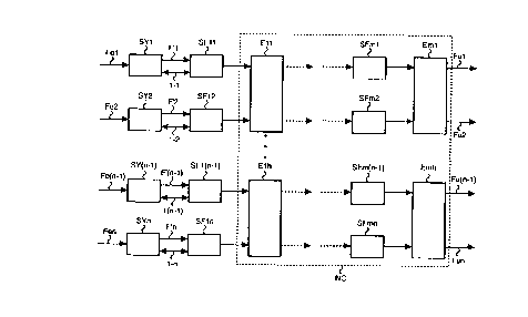
In Figure 1, NC is the connection network of an optical ATM switching
node with n inputs and n outpus connected to respective optical fibers Fe
1...Fen,
Ful...Fun. The node comprises) in the most general case, ~ stages composed of
elements
E 11...E 1 h...Em 1...Emh that, purely as an example, are represented as
elements with two
inputs and two outputs. The structure of the node and of the switching
elements has no
interest for the purposes of the present invention. In general, at any rate,
current ATM
optical nodes comprise an optical connection network and an electrical control
structure;
the latter one is not indicated in the Figure because it is not influenced by
the invention.
Input fibers Fel...Fen are associated to devices SY1...SYn which perform a
phase
realignment of the cells, by discrete steps. The cells phase-realigned by
devices SY are
supplied through fibers F'1...F'n to fine synchronization devices SF1...SFn
aimed to
continuously compensate for remaining phase shifts. Furthermore, since
response times
of devices SY are relatively long, as will be better seen afterwards) devices
SF are also to
operate in place of devices SY in the periods when these latter ones respond
to the
detection of a phase shift. In order to allow cooperation, devices SY, SF will
exchange
information through connections 1-1...1-n. Fine synchronization devices
SFml...SFmh
are also associated with the inputs of the stages following the first one in
node NC,to
compensate possible optical path differences of the cells between a stage and
the
following one.
_ 214581 ~
Devices SF can be of the type described in the already mentioned Italian
Patent Application.
Fig. 2 shows a preferred embodiment of a device SY. For this
embodiment, let us assume that ATM cell flows incoming to the node are
substantially
5 continuous flows, apart from a guard time between subsequent cells that is
necessary to
enable setting of the node elements and operation of the synchronization
device, as will
be better explained below. As an example) where necessary, reference will be
made to a
transmission at 622 Mbit/s, with cells formed by 64 bytes, so that every bit
lasts 1.6 ns.
The guard time can for example be 7 bytes long (therefore about 100 ns),
within the 64
bytes.
As can be seen in the Figure) fiber Fe is connected to an optical delay line
LR with variable delay, capable of delaying the incoming signal for the time
necessary to
realign the cell with a local reference signal (hereinafter also called
"synchronization
signal"). The delay line LR is a so-called logarithmic delay line, realized
through optical
switches CL1...CLx with two inputs and two outputs, that send signals either
on a direct
path Z1...Zx, whose delay can be considered null, or on a delay element
R1...Rx, that
delays signals travelling through it by a fixed time that is progressively
decreasing
according to a constant ratio, in particular equal to 2. Paths Z1...Zx and
elements
R1...Rx are optical fiber spans of suitable lengths. The delay introduced by
the last delay
element Rx of the line is a fraction of the maximum delay that can be
compensated by
devices SF, to allow overlapping between the operations of the two devices.
For
example, if devices SF compensate phase shifts up to one bit time ( 1.6 ns in
the example
taken into account), the delay introduced by Rx can be 1/4 of the bit time
(400 ps). The
number of switches CL1...CLx and therefore of delay elements RI...Rx will
obviously
determine the maximum phase shift that can be compensated by LR. In practice)
11
elements R1...Rx can be employed, with delays ranging from 1/2 cell (256 bits,
about
400 ns) to 1/4 bit, so that delays included between about 0 and 800 ns ( 1
cell) can be
compensated by steps of 400 ps.
Optical switches CL1...CLx) that can be controlled individually and
independently from one another, have no particular speed requirements and are
for
example thermo-optical couplers. These switches have a switching time of the
order of a
few milliseconds. Switching of switches CL1...CLx is controlled by signals
supplied
through wires 3-1...3-x by driversDR, which bring to the level necessary for
the switch
control, the bits composing a digital error signal ER supplied through a
connection 2 by
a circuit VE determining the phase shift entity. In particular, as will be
better seen below,
every bit in signal ER is associated with one of switches CL and causes that
switch to be
6 2145817
set to a straight position for example when the bit has logic value 0 and to a
cross
position when it has logic value 1.
The last delay element Rx and the last direct path Zx are connected to the
two inputs of a further, relatively fast optical switch (or Y coupler) CV) for
example a
LiNB03 switch. Such a switch has a switching time less than 1 ns. Switching of
CV is
controlled by a signal supplied by drivers DR through a wire 4 and obtained
from a signal
SW emitted by VE: value 0 of such signal causes for example switching of CV on
the
input connected to path Zx, while value 1 causes switching of CV on the input
connected
to the element Rx. Also the two positions of CV will be denoted as straight
and cross
positions. Use of switches like CV within a delay line is not convenient, both
because
they are much more expensive than the thermo-optical couplers) and because
they are
sensitive to optical signal polarization, whose maintenance along delay line
LR cannot be
guaranteed by using conventional fibers and would require use of polarization
maintaining fibers that are much more expensive.
The output of CV is connected to an optical amplifier AM, that
compensates attenuations introduced by delay line LR and is followed by an
asymmetric
power divider RP1 that sends a small fraction (for example 1/10) of the
optical signal
power associated with a cell to a detector RIC of the beginning of a cell)
through a fiber
span fl. The remaining power is sent to output F' of device SY.
Detector RIC can be realized as described in the above-mentioned Italian
Patent Application, and is based on the recognition of an initial cell word,
in particular a
4- bit word. Its structure will be described with reference to Fig. 3.
Detector RIC
generates a signal IC representing the occurred recognition) that is sent to
circuit VE and
to a circuit having the same functions as VE in device SF through a wire 1 a
of one of the
respective connections 1 (1- 1...1-n).
Circuit VE determines the entity of the phase shift between cell-beginning
signal IC and a local reference or synchronization signal SS 1, that is the
same for all
devices SY and is supplied by the time base of the node (not shown). For its
operation)
VE receives through wires lb of connection 1 information about the phase shift
entity
measured by the homologous device in SF. As will be seen after, circuit VE is
realized so
that in steady state conditions the error signal compensates possible phase
shifts through
actuation of a single switch CL.
In Fig. 3, device RIC includes a second power divider RP2 that shares the
power present on fl among four different outputs connected to respective
optical fiber
spans f2...f5. The four fiber spans have such a length that signals go out of
f3, f4, f5 with
a delay respectively exceeding by 1, 2 or 3 bit times the delay introduced by
f2. Fiber
spans f2...f5 form therefore an optical series-to-parallel converter SP. The
four bits of the
215817
initial word are detected in parallel in as many detectors represented within
block RIV
and, after having been converted into logic signals by threshold decision
circuits DS, are
supplied to a comparator COM that compares the pattern present at the output
of RIV
with the pattern foreseen for the initial word) read in a memory ME. Should
the
comparison outcome be positive, comparator COM sends a signal with an adequate
logic
level (for example level 1). The output of COM is connected to a contml
circuit CC, that
must verify that the word recognized by the comparator is really the initial
word and not
an identical pattern present in the data in a cell. For example, CC will send
on output
wire la the cell beginning signal IC only if COM has issued a "1" signal for a
predefined
i0 number of times (for example 4) at intervals of one cell time. For this
purpose, CC will
have to receive synchronization signal SS 1. Devices like CC are well known in
the art.
Fig. 4 shows a preferred embodiment of device VE. The device includes a (x-2)-
bit counter CN 1 that is started by the synchronization signal S S 1 and is
stopped by the
cell beginning signal IC (or vice versa) and counts the pulses of a clock
signal CK at the
transmission rate on fiber Fe. Counter CN 1 then evaluates phase shift between
the two
signals with the precision of one bit time. Preferably, CN1 is realized so
that the binary
value read at the count stop instant represents the delay to be introduced on
the cell to
obtain realignment with the synchronization signal. The count reached by CN 1
at the
stop instant is loaded into a first x- position register RG1, that loads into
the two least
2o significant positions a pair of bits supplied by an analog-to-digital
converter AN that
converts into digital signals the phase shift value measured by device SF.
With such an
arrangement, each one of the x bits in RG 1 is associated with one of the
elements
Ra...Rx and indicates, when it is at 1, that the associated element must be
inserted along
the optical signal path. The content of RG 1 is supplied to ad adder S M where
it is added
to the value contained in a second register RG2, where the phase shift
compensated up
to the immediately preceding cell is stored. The result of the addition is
loaded into RG2
to update the content thereof. Adjacent bits of the content of RG2 are
combined in
exclusive OR in a combinational network EX to generate the error signal ER,
composed
of x bits that are presented on a first group 2a of wires of connection 2. The
least
significant bit of the value stored in register RG2 will further be
transformed into
command SW for CV, through AND gates A1 and A2, a set-reset flip-flop FF1
(that
receives this bit at its set or reset input depending on the logic value being
1 or 0) and a
D flip-flop FF2.
The bits stored in RG 1 are also supplied to a phase shift recognition
device RS, in practice a logic NOR gate, that recognizes that at least one bit
in RG 1 is
different from 0. In case of a phase shift, RS generates a signal that starts
the count, by a
counter CN2, of a time T 1 sufficient to guarantee that more than 50% of the
optical
g 2145817
power is present on the desired output of switches CL1...CLx (for example a 3
ms time).
The signal generated by RS is supplied to CN2 after having been delayed in a
delay
element RT by the time necessary to perform the addition in SM and to update
RG2. The
signal going out of RT also disables counter CNl: this is necessary since
device SY is
able to process a new cell only after switching of switches CL (Fig. 2). The
terminal
count signal of CN2 enables transferring the least significant bit of RG2 to
FF1 through
gates A 1, A2. The actual signal SW is then generated through FF2) to enable
switching
of CV during the guard time between two consecutive cells, which is signalled
by a
second synchronization signal SS2 also generated by the system time base. The
terminal
count signal of CN2 also enables again counter CNl.
Operation of the invention will now be described) referring, for the sake
of simplicity, to an example in which LR includes 5 delay elements R1...R5
that introdu
ce delays from 400 ps to 6.4 ns (from 1/4 of the bit time to 4 bit times), so
that LR is
able to compensate phase shifts up to 12.8 ns. For the operation, a
distinction must be
made between a transient period, corresponding to the beginning of a
transmission on the
line concerned and during which even important phase shifts will have to be
compensated, and a steady state condition, in which phase shifts are supposed
to be
limited and slowly variable: this is typical) for example, of phase shifts due
to thermal
drifts. As long as the initial phase shift is not compensated, all cells will
be lost.
Let us suppose that initially switches CL1...CLS are arranged in a straight
configuration, so that incoming signals on fiber Fe are forwarded along null-
delay paths
Z1...Zx and therefore they immediately reach the phase shift determining
devices.
Obviously CV too will be in a straight position. The first operation to be
performed is
locking device SY to cell synchronism SS 1. Locking is obtained when control
circuit CC
in device RIC (Fig. 3) has recognized the initial bit pattern, for the
predefined number of
times, at intervals corresponding to the cell period. After such locking has
been achieved,
SY is actually able to operate. The first signal IC starts CNl which counts
the pulses of
CK till the instant shown by SS 1. Let us suppose that phase shift is 4.5 ns
(that is a phase
shift between 2 and 3 bits and more precisely between 2 3/4 bits and 3 bits).
The value
read in CN1 at that moment will be 010 and the pair of bits supplied by SF
will be 11:
these 5 bits are loaded into RG 1 and are stored unmodified in RG2 and
transformed by
EX into error signal 01110) that sets CL2) CL3, CL4 to cross position, while
CL1 and
CLS remain in straight position: the cells therefore follow the path Zl, R2,
Z3, R4, RS
that inserts a global delay of 4.4 ns (3.2 ns, that is 2 bits, in R2, 1/2 bit
= 0.8 ns in R4 and
1/4 bit = 0.4 ns in RS). A phase shift having been recognized) the count of
time T1 is
started. At the end of the count of Tl, the least significant bit of RG2 is
transferred to
the output of FF 1 through gate A 1 to generate S W. Since this bit is 1, CV
is set to cross
_2145817
position, and therefore it actually transfers to its output the signals coming
out of the last
delay element. From that instant on, the cells going out of LR are in phase
with SS 1)
apart from the remaining phase shift of 0.1 ns that is compensated by SF, and
the steady
state condition is reached.
For the first cell arriving at RIC after the steady state condition has been
reached, register RG 1 will contain all 0's; the content of RG2 and the
position of
switches CL) CV do not change. The situation remains unchanged as long as the
phase
shift between signals IC and SS 1 if any, remains less than 1/4 of a bit time:
SY does not
intervene and possible variations of the instants of arrival of the cells are
compensated by
SF. If at a certain instant the phase shift reaches 1/4 of the bit time
(taking the global
phase shift to 4.9 ns), the least significant bit supplied by AD becomes 1.
Pattern 00001
is now present in RG 1 and, when added to the one present in RG2 (01011 ),
results in a
new pattern 01100 that is transformed by EX into the new error signal 01010.
Consequently) switch CL3 is set to the straight position and the cells now
follow path
Z1, R2, R3, Z4, ZS that compensates a 4.8 ns phase shift. The remaining 0.1 ns
phase
shift is compensated by SF as above.
As it can be noted, only one bit has changed in error signal ER with
respect to the previous pattern, in particular the bit associated with the
third switch CL3)
that will be set to a straight position in order to insert delay element R3.
As a
consequence of the change of position in CL3) R4 and R5, that were previously
inserted,
will remain cut off. Furthermore, the least significant bit in RG2 has become
0, and this
corresponds to extracting the signal from Z5. As during the transient time)
adder SM is
inhibited during switching time Tl of switches CL and therefore SY does not
carry out
any action on the cells following the one taken into account) till after the
possible CV
switching. However, even during that time, part of the power goes on striving
to divider
RP1 along the previous path and it is supplied to SF, that compensates the
detected
phase shift: since the optical signal path variation has been supposed to be
much slower
than the switching time of switches CL, the phase shift will surely be within
the operation
range of SF.
It is immediately apparent that, with the described arrangement, if a slow
phase shift variation is assumed) whichever the configuration assumed by
switches CL to
compensate the initial phase shift, under steady state conditions, the
variation of a single
thermo-optical switch always occurs upon the least significant bit in RG 1
becoming 1.
This allows obtaining the phase realignment without losing information, in
spite of the
switches CL being slow. Should more than one switch be actuated, a
superimposition of
differently delayed replicas of the same cell would occur, making it
impossible to process
the cell within the node.
_.: ~ 1~ _ 214581 ~
It is obvious that what has been described has been given only as a non-
limiting example
and that variations and modifications are possible without departing from the
scope of
the invention, particularly as regards the realization of electronic circuits.