Note: Descriptions are shown in the official language in which they were submitted.
2~.~~9~a
RCA 87,591
-1-
MEDIA ERROR CODE GENERATION AS FOR A
V117E0 INVERSE TRANSPORT PROCESSOR
This invention relates to a method and apparatus for
inserting medial error codes in packets of compressed video signal
for alerting a video signal decompressor to reset to a
predetermined state.
It is known from, for example, United States Patent No.
5,168,356 that it is advantageous to transmit compressed video
signal in packets, with respective packets including a measure of
error correction. Television receivers designed to decompress
transmitted packeted compressed video signal may not receive
the entire sequence of transmitted packets. In the absence of a
packet in the received signal, it is known from United States
Patent No. 5,289,276 to insert a media error code in the signal
1 S stream for a lost packet, which media error code will condition the
decompression circuitry to reset at a predetermined signal entry
point at which the decompressor can reliably continue
decompression.
Apparatus for performing the inverse packeting
2 0 process, at least for high definition television (HDTV) signals must
operate a extremely high speed to process the relatively high data
rates of a HDTV signal. The present inventors, in designing
inverse packet processors found it extremely difficult to arrange
apparatus to include media error codes after detecting that a.
2 S particular packet had been lost in transmission. The present
invention solves the problem of inserting media error codes in a
non-complicated manner, without incurring any timing constraints
over those constraints associated with simple inverse packet
processing.
3 0 The present invention is apparatus in an inverse
transport processor of the type which directs the video payloads
of respective packets to buffer memory space, for writing a media
error code at sequential first memory address locations ahead of
each packet payload while the processor is checking for lost
3 S packets. If a packet is lost, the payload is written to memory in
subsequent sequential address locations. If there is no loss of
packet, the sequential first memory address locations are simply
overwritten by the packet payload to excise the undesired media
error code.
_ _2_
RCA 87,591
BRIEF DESCRIPTION OF THE DRAWINGS
The invention will be described with reference to the
drawings, wherein:
FIGURE 1 is a pictorial representation of a time
division multiplexed packet television signal;
FIGURE 2 is a pictorial representation of respective
signal packets;
FIGURE 3 is a block diagram of a receiver for selecting
and processing packets of multiplexed component signals
embodying the present invention;
FIGURE 4 is a block diagram of exemplar memory
management circuitry which may be implemented for element 17
of FIGURE 3; and
1 5 FIGURE 5 is a block diagram of exemplary lost packet
detection circuitry.
FIGURE 1 shows a signal stream consisting of a string
of boxes which represent signal packets which are components of
2 0 a plurality of different television or interactive television
programs. These program components are assumed to be formed
of compressed data and as such the quantity of video data for
respective images is variable. The packets are of fixed length.
Packets with letters having like subscripts represent components
2 5 of a single program. For example, V;, A;, D; represent video, audio
and data packets and packets designated Vl, A1, D1, represent
video, audio and data components for program 1, and V3, A31, A32
D3, represent video, audio 1, audio 2 and data components of
program 3. In the upper line of the string of packets the
3 0 respective components of a particular program are shown grouped
together. However there is no necessity of packets from the same
program being grouped as is indicated by the packet sequence
shown in the middle of portion of the string of packets. Nor is
there any particular order for the sequence of occurrence of
3 5 respective components.
The respective packets are arranged to include a
prefix and a payload as shown in FIGURE 2. The prefix of this
example includes two 8-bit bytes comprising five fields, four (P,
2i~~~~~
_ _3_
RCA 87,591
BB, CF, CS) of which are 1-bit fields, and one (SCID) of which is a
12-bit field. The SCID field is the signal component identifier.
The field CF contains a flag to indicate whether the payload of the
packet is scrambled, and the field CS contains a flag which
indicates which of two alternative unscrambling keys is to be
utilized to unscramble scrambled packets. The prefix of every
packet is packet aligned, thus the location of the respective fields
are easily identifiable.
Within every payload is a header which contains a
1 0 continuity count, CC, modulo 16, and a TOGGLE flag bit which are
program component specific. The continuity count is simply a
successive numbering of sequential packets of the same program
component. The TOGGLE flag bit, in video component packets, is a
one bit signal which changes logic level or toggles at the
occurrence of a picture layer header, that is at the beginning of a
new frame.
FIGURE 3 illustrates in block form a packet
detector/selector of a digital television receiver. Signal is detected
by an antenna 10 and applied to a tuner detector, 11, which
2 0 extracts s a particular frequency band of received signals, and
provides baseband compressed signal in a binary format. The
frequency band is selected by the user through a microprocessor
19 by conventional methods. Nominally broadcast digital signals
will have been error encoded using, for example, Reed-Solomon
2 5 forward error correcting {FEC) coding. The baseband signals will
thus be applied to a FEC decoder, 12. The FEC decoder 12 will
synchronize the received video and provide a stream of signal
packets of the type illustrated in FIGURE 1. The FEC 12 may
provide packets at regular intervals, or on demand, by for
3 0 example, memory controller 17. In either case a packet framing
or synchronizing signal is provided by the FEC circuit, which
indicates the times that respective packet information is
transferred from the FEC 12.
The detected frequency band may contain a plurality
3 5 of time division multiplexed programs in packet form. To be
useful, only packets from a single program should be passed to
the further circuit elements. In this example it is assumed that
the user has no knowledge of which packets to select. This
RCA 87,591
-4-
information is contained in a program guide, which in itself is a
program consisting solely of data which interrelates program
signal components through SCID's. The program guide is a listing
for each program, of the SCID's for the audio, video, and data
S components of respective programs. The program guide (packets
D4 in FIGURE 1) is assigned a fixed SCID. When power is applied
to the receiver, the microprocessor 19 is programmed to load the
SCID associated with the program guide into one of a bank of
similar programmable SCID registers 13. The SCID field of the
prefix portion of respective detected packets of signal from the
FEC 12 are successively loaded in a further SCID register 14. The
programmable registers and the received SCID register are
coupled to respective input ports of a comparator circuit 15, and
the received SCID is compared with the program guide SCID. If
1 5 the SCID for a packet matches the program guide SCID, the
comparator 15 conditions a memory controller 17 to route that
packet to a predetermined location in the memory 18 for use by
the microprocessor. If the received SCID does not match the
program guide SCID, the corresponding packet is simply dumped.
2 0 The microprocessor waits for a programming
command from the user via an interface 20, which is shown as a
computer keyboard but which may be a conventional remote
control, or receiver front panel switches. The user may request to
view a program provided on channel 4 (in the vernacular of
2 5 analog TV systems). The microprocessor 19 is programmed to
scan the program guide list that was loaded in the memory 18 for
the respective SCID's of the channel 4 program components, and to
load these SCID's in respective other ones of the programmable
registers of the bank of registers 13 which are associated with
3 0 corresponding component signal processing paths.
Received packets of audio, video or data program
components, for a desired program, must ultimately be routed to
the respective audio 23, video 22, or auxiliary data 21, (24) signal
processors respectively. The exemplary system of FIGURE 3, first
3 5 routes the respective packets to predetermined memory locations
in the memory 18. Thereafter the respective processors 21-24
request the component packets from the memory 18. It should be
appreciated that the signal components are compressed and that
RCA 87,591
_ -5-
decompression devices do not require input data on a continuous
basis. Routing the components through the memory provides a
measure of desired signal throttling.
The audio, video and data packets are loaded into
predetermined memory locations to enable the signal processors
easy access to the component data. In order that the appropriate
packets get loaded in the appropriate memory areas, the
respective SCID comparators must be associated with those
memory areas. This association may be hardwired in the memory
controller 17, or the association may be programmable. If the
former, specific ones of the programmable registers will always be
assigned the audio, video and data SCID's respectively. If the
latter the audio, video and data SCID's may be loaded in any of the
programmable registers, and the appropriate association be
programmed in the memory control 17 when the respective SCID's
are loaded in the programmable registers.
In the steady state, after the program SCID's have
been stored in the programmable registers 13, the SCID's of
received signal packets are compared with all of the SCID's in the
2 0 programmable SCID registers. If a match is made with either a
stored audio, video or data SLID, the corresponding packet
payload will be stored in the audio, video or data memory area
respectively.
The respective signal packets are coupled from the FEC
2 5 12 to the memory controller 17 via a signal decryptor 16. Only
the signal payloads are scrambled. Whether or not a packet is to
be descrambled is determined by the CF flag in the packet prefix,
and how it is to be descrambled is determined by the CS flag. If
no SCID match is had for a respective packet, the decryptor may
3 0 simply be disabled from passing any data. Alternatively, if there
is no SCID match for a packet the decryptor may be allowed to
decrypt according to its last settings and the memory write
control may be disabled to dump the respective packet.
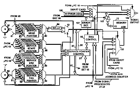
FIGURE 4 illustrates exemplary apparatus for the
3 5 memory controller 17 shown in FIGURE 3. Each program
component is stored in a different contiguous block of the memory
18. In addition other data, such as data generated by the
RCA 87,591
-6-
microprocessor 19 or a Smart Card (not shown) may be stored in
the memory 18.
Addresses are applied to the memory 18 by a
multiplexor 105, and input data is applied to the memory 18 by a
multiplexor 99. Output data from the memory management
circuitry is provided to the signal processors by a further
multiplexor 104. Output data provided by the multiplexor 104 is
derived from the microprocessor 19, the memory 18 or directly
from the multiplexor 99. Program data is presumed to be of
standard picture resolution and quality, and occurring at a
particular data rate. On the other hand high definition television
signals, HDTV, which may be provided by this receiver, occur at a
significantly higher data rate. Practically all data provided by the
FEC will be routed through the memory 18 via the multiplexor 99
1 5 and memory I/O circuit 102, except for the higher rate HDTV
signals which may be routed directly from the multiplexes 99 to
the multiplexor 104. Data is provided to the multiplexes 99 from
the decryptor 16, the smart card circuitry, the microprocessor 19,
and a source of a media error codes 100. The term "media error
2 0 codes" as used herein, mean special codewords to be inserted in a
data stream, to condition the respective signal processor
(decompressor) to suspend processing until detection of a
predetermined codeword such as a start code, and then to resume
processing in accordance with the e.g. start code.
2 5 Memory addresses are provided to the multiplexor
105, from program addressing circuitry 79-97, from the
microprocessor 19, from the Smart Card apparatus (not shown)
and possibly from other auxiliary devices. Selection of the
particular address at any particular time period is controlled by a
3 0 direct memory access DMA, circuit 98. The SCID control signals
and "data needed" signals from respective signal processors are
applied to the DMA 98, and responsive thereto, memory access
contention is arbitrated. The DMA 98 cooperates with a Service
Pointer Controller 93, to provide the appropriate read or write
3 5 addresses for respective program signal components.
The respective addresses for the various signal
component memory blocks are generated by four groups of
program component or service pointer registers 83, 87, 88, and
RCA 87,591
_7_
92. The starting pointers for respective blocks of memory, into
which respective signal components are stored, are contained in
registers 87 for the respective signal components. The start
pointers may be fixed values, or they may be calculated by
conventional memory management methods in the microprocessor
19.
The last address pointers for respective blocks are
stored in the bank of service registers 88, one for each potential
program component. Similar to the start addresses, the end
addresses may be fixed values or they may be calculated values
provided by the microprocessor 19. Using calculated values for
starting and end pointers is preferred because it provides a more
versatile system with less memory.
The memory write pointers or head pointers are
generated by the adder 80 and the service head registers 83.
There is a service head register for each potential program
component. A write or head pointer value is stored in a register
83, and provided to the address multiplexor 105 during a memory
write cycle. The head pointer is also coupled to the adder 80,
2 0 wherein it is incremented by one unit, and the incremented
pointer is stored in the appropriate register 83 for the next write
cycle. The registers 83 are selected by the service pointer
controller, 93, for the appropriate program component currently
being serviced.
2 5 In this example it is assumed that the start and end
pointers are 16-bit pointers. The registers 83 provides 16 bit
write or head pointers. The memory 18, on the other hand has
18-bit addresses. The 18-bit write addresses are formed by
concatenating the two most significant bits of the start pointers to
3 0 the 16-bit head pointers, with the start pointer bits in the most
significant bit positions of the combined 18-bit write address. The
start pointers are provided by the respective registers 87 to the
service pointer controller 93. The service pointer controller
parses the more significant start pointer bits from the start
3 5 pointers stored in registers 87, and associates these bits with the
16-bit head pointer bus. This is illustrated by the bus 96 shown
being combined with the head pointer bus exiting the multiplexor
85.
2~.~~~(l0
_g_
RCA 87,591
Similarly, memory read pointers or tail pointers are
generated by the adder 79 and the service tail registers 92. There
is a service tail register for each potential program component. A
read or tail pointer value is stored in a register 92, and provided
to the address multiplexor 105 during a memory read cycle. The
tail pointer is also coupled to the adder 79, wherein it is
incremented by one unit, and the incremented pointer is stored in
the appropriate register 92 for the next read cycle. The registers
92 are selected by the service pointer controller, 93, for the
appropriate program component currently being serviced.
The registers 92 provides 16 bit tail pointers. 18-bit
read addresses are formed by concatenating the two most
significant bits of the start pointers to the 16-bit tail pointers,
with the start pointer bits in the most significant bit positions of
the combined 18-bit write address. The service pointer controller
parses the more significant start pointer bits from the start
pointers stored in registers 87, and associates these bits with the
16-bit tail pointer bus. This is illustrated by the bus 94 shown
being combined with the tail pointer bus exiting the multiplexor
2 0 90.
Data is stored in the memory 18 at the calculated
address. After storing a byte of data, the head pointer is
incremented by one and compared to the end pointer for this
program component, and if they are equal the more significant
2 5 bits of the head pointer are replaced with the lower 14 bits of the
start pointer and zeros are placed in the lower two bit positions of
the head pointer portion of the address. This operation is
illustrated by the arrow 97 pointing from the service pointer
controller 93 to the head pointer bus from the multiplexor 85. It
3 0 is presumed that application of the lower 14 start pointer bits
override the head pointer bits. Replacing the head pointer bits
with the lower start pointer bits in the address for this one write
cycle, causes the memory to scroll through the memory block
designated by the upper two start pointer bits, thus obviating
3 5 reprogramming write addresses at the start of each packet to a
unique memory location within a block.
If the head pointer ever equals the tail pointer (used
to indicate where to read data from the memory 18) a signal is
RCA 87,591
-9-
sent to the interrupt section of the microprocessor to indicate that
a head tail crash has occurred. Further writing to the memory 18
from this program channel is disabled until the microprocessor re-
enables the channel. This case is very rare and should not occur
in normal operation.
Data is retrieved from the memory 18 at the request
of the respective signal processors, at addresses calculated by the
adder 79 and registers 92. After reading a byte of stored data,
the tail pointer is incremented by one unit and compared to the
end pointer for this logical channel in the service pointer
controller 93. If the tail and end pointers are equal then the more
significant bits of the tail pointer are replaced with the lower 14
bits of the start pointer and zeros are placed in the lower two bit
positions of the tail pointer portion of the address. This is
illustrated by the arrow 95 emanating from controller 93 and
pointing to the tail pointer bus from the multiplexor 90. If the tail
pointer is now equal to the head pointer then the respective
memory block is defined as empty and no more bytes will be sent
to the associated signal processor until more data is received from
2 0 the FEC for this program channel. The actual replacement of the
head or tail pointer portions of the respective write or read
addresses by the lower 14 bits of the start pointer may be
accomplished by appropriate multiplexing, or the use of three
state interconnects
2 5 It will be appreciated by those skilled in the art of
digital signal processing that the combination of memory and
addressing circuitry utilized above effectively conditions the
random access memory 18 to operate as a plurality of first-in-
first-out memories or FIFO's
3 0 Memory read/write control is performed by the
service pointer controller and direct memory access, DMA,
elements 93 and 94. The DMA is programmed to schedule read
and write cycles. Scheduling is dependent upon whether the FEC
12 is providing data to be written to memory or not. FEC data
3 5 write operations take precedence so that no incoming signal
component data is lost. In the exemplary apparatus illustrated in
FIGURE 4, there are four types of apparatus which may access the
memory. These are Smart Card (not shown), the FEC 12 (more
-10-
RCA 87,591
precisely the decryptor 16), the microprocessor 19 and one of the
application devices such as the audio and video processors.
Memory contention is handled in the following manner. The DMA,
responsive to data requests from the various processing elements
listed above, allocates memory access as follows. Access to the
memory is provided in 95 nS time slots during which a byte of
data is read from or written to the memory 18. There are two
major modes of access allocation, defined by "FEC Providing Data",
or "FEC Not Providing Data" respectively. For each of these modes
the time slots are allocated and prioritized as follows, assuming a
maximum FEC data rate of 5 Mbytes/second, or one byte for each
200 nS. These are:
FEC Providin Data
1 ) FEC data write;
2) Application device read/Microprocessor read/write;
3) FEC data write;
4) Microprocessor read/write;
and for
FEC Not Providin Data
2 0 1) Smart Card read/write;
2) Application device read/Microprocessor read/write;
3 )Smart Card read/write;
4) Microprocessor read/write.
Because FEC data writes cannot be deferred, the FEC (or more
2 5 correctly the decryptor), when providing data must be guaranteed
memory access during each 200 nS interval. Alternate time slots
are shared by the application devices and the microprocessor.
When there is no data available for the requesting devices, the
microprocessor is provided use of the application time slots.
3 0 The Controller 93 communicates with the SCID
detector to determine which of the respective Start, head and end
pointer registers to access for memory write operations. The
controller 93 communicates with the DMA to determine which of
the start, end and tail registers to access for memory read
3 5 operations. The DMA 98 controls selection of the corresponding
addresses and data by the multiplexers 99, 104 and 105.
As stated earlier, it is advantageous to insert media
error codes into the video component signal stream when packets
~- ~ ~ ~ ~ ~ RCA 87,591
-11-
are lost, to condition the video signal decompressor to suspend
decompression until a particular signal entry point occurs in the
data stream. It is not practical to predict where and in which
video packet the next entry point may occur. In order to find the
next entry point as fast as possible, it is necessary to include a
media error code at the beginning of the first video packet after
detection that a packet is lost. The circuitry of FIGURE 4 places a
media error code at the beginning of every video packet and then
excises the media error code in respective packets if there is no
loss of a preceding packet. The media error code is inserted in the
first M memory address locations reserved for the current video
packet payload, by writing to memory 18 for M write cycles prior
to the video payload arriving from the decryptor. Concurrently
the multiplexor 99 is conditioned by the DMA 98, to apply the
1 5 media error code from the source 100 to the memory 18 I/O. M is
simply the integer number of memory locations required to store
the media error code. Assuming the memory to store 8-bit bytes,
and the media error code to be 32 bits, M will equal 4.
The addresses for loading the media error code in
2 0 memory are provided by the respective video component service
register 83 via the multiplexes 82 and multiplexes 85. It will be
appreciated that the first M addresses provided from the pointer
register 83 for loading the media error code into the memory
locations that would otherwise be loaded with video component
2 5 data, will simply be the next M sequential addresses that would
normally be produced by the video head pointer. These same
addresses are coupled into an M-stage delay element 84, so that
immediately after the last byte of the media error code is stored
in the memory 18, the first of the M addresses is available at the
3 0 output of the delay element 84.
The timing of the loading of the media error code into
memory coincides with the determination of a lost packet.
Loading the media error code while packet loss determination is
performed places no additional timing constraints on signal flow
3 5 processing. Packet error or loss detection is performed by an
error detector 101 which is responsive to the CC and HD data of
the current packet. The detector 101 examines the continuity
count CC in the current packet to determine if it differs from the
2~~~~~4
RCA 87,591
-12-
CC of the previous packet by one unit. In addition the TOGGLE bit
in the current packet is examined to determine if it exhibits a
different state from the TOGGLE bit of the previous packet. If
either of these conditions are not satisfied, a packet error has
occurred, and the media error code may be retained in memory
for the current packet to reset the video decompressor. The
preferred criterion for determining packet loss is for both of the
above conditions not to be satisfied.
If a packet loss is detected, the video component of the
current packet is stored in memory 18, starting at the next or
(M+1 )th address location. This is accomplished by conditioning
the multiplexer 85 to continue to pass undelayed head pointers
from the appropriate register 83. Alternatively, if a packet loss is
not detected, the first M bytes of the video component in the
current packet are stored in the memory locations in which the
media error code was immediately previously stored. This is
accomplished by the service pointer controller conditioning the
multiplexer 85 to pass the delayed head pointers from the delay
element 84, for M write cycles. At the end of the M write cycles
2 0 the service pointer controller 93 will condition the multiplexer to
again pass undelayed head pointers. When the multiplexer
switches back to non delayed pointers, the next non delayed
pointer will correspond to the . M+lth address.
Depending upon the particular designs of a given
2 S receiver, it may or may not be conducive to include media error
codes in different ones of the signal components when respective
component transport packets are lost. In addition it may be
advantageous to utilize different media error codes for different
signal component formats or compression processes. Thus one or
3 0 more media error code sources may be required. Regardless of
the number and/or type of media error codes needed, the
foregoing method of including a media error code with every
packet, and then overwriting the media error code if it is not
actually needed, is an extremely advantageous approach to the
3 5 problem of inserting the codes.
FIGURE 5 illustrates exemplary circuitry for detecting
lost packets. The hardware elements may however be realized in
software within a microprocessor which may be used to control
~1~ ~~Qd
-13-
RCA 87,$91
the memory management apparatus. In FIGURE 5, timing
circuitry 201, responsive to the packet framing pulse provided by
the FEC and a byte clock, generates a positive going transition
during the period the third byte of the current packet is available
from the decryptor. This positive going transition loads the third
data byte into the one of the byte registers 205 selected by the
SCID detector control signal. The byte loaded in the register 205
includes the continuity count bits, CC, and the TOGGLE bit in the
service header of the packet. The CC bits and the TOGGLE bit
loaded into register 205 are respectively compared, in the
comparators 206A and 206B, with similar bits in the appropriate
one of the registers 202 selected by the SCID detector control
signal. The output connections of the comparators 206A and 206B
are coupled to the memory controller 17, which is responsive to
the condition of these signals to effect certain remedial action in
the event of mismatch.
The values in register 202 are generated as follows.
The continuity count, CC, of successive packets of the same signal
component increment by one unit for each successive packet,
2 0 hence each sequential CC value is one unit greater than the prior
value. The CC of the current packet is applied to the input of an
adder 203 wherein it is incremented by one unit so that it equals
the value of the next expected CC value for the component. The
incremented value from the adder 203 is stored in the register
2 5 202, addressed according to the received SCID, for use in
comparing the CC of the next payload.
The TOGGLE bit for the video component, on the other
hand, is the same for all packets in a frame, and changes state in
the packet containing a picture layer header. Each successive
3 0 TOGGLE bit is stored unchanged in the appropriate register 202.
At the termination of the current packet, the timing
circuit 201 generates a pulse which conditions the register 202 to
store the incremented CC value from the current packet, and the
TOGGLE bit from the current packet, in the appropriate register
3 S 202. These CC and TOGGLE bit values correspond to the CC and
TOGGLE bit values expected in the next packet of the same signal
component.
214900
RCA 87,591
-14-
The memory controller monitors the output of the
comparator 206A for CC mismatch detection. If a mismatch in the
CC values is indicated, then the output of the comparator 206B is
examined for TOGGLE mismatch. If a mismatch has occurred in
both the CC and TOGGLE values, a first mode of remedial action is
initiated. If a mismatch has occurred only in the CC value, a
second mode of remedial action is initiated. The first mode causes
the transport processor to search for the next occurring packet
containing a picture layer header. This packet may be at the
beginning of the next frame of data, or it may be a packet
especially arranged to contain redundant picture layer header
data. See for example United States Patent 5,289,276. The
processor will recommence passing video component data to the
memory 18 starting with the first packet containing the picture
layer header.
In the second mode, the presumption is made that a
less severe data loss has occurred, and it is not necessary to reset
processing on a frame boundary. Rather processing is reset to a
slice boundary. For the definition of a slice the reader is referred
2 0 to GENERIC CODING OF MOVING PICTURES AND ASSOCIATED
AUDIO, Recommendation H.262, ISO/IEC 13818-2 Committee Draft
(International Standardisation Organization). Resetting to a slice
boundary is initiated by causing the system to not pass further
video component data to memory 18 until occurrence of the next
2 5 packet which contains an MPEG start code.
The packets containing the picture layer header or the
slice start code are detected via the programmable matched filter
09. Filter 09 is conditioned by the memory controller 17 to detect
packets containing the one or the other of picture layer or slice
3 0 layer start codes, responsive to one or both of the comparators
206A and 206B indicating mismatch respectively.
It should be noted that at each packet containing a
picture layer header the comparator 206B will produce an
erroneous mismatch because the TOGGLE bit changes in these
3 5 packets. This is of no consequence. The mismatch of the TOGGLE
bit only comes into play if the CC's are also mismatched, and then
it only effects conditioning of the system to reset to a packet
containing a picture layer header. Such action will of necessity be
2I~~9~~
- -15-
RCA 87,591
required if there is a CC mismatch for the packet containing the
picture layer header whether or not there is an erroneous TOGGLE
bit mismatch.
S