Note: Descriptions are shown in the official language in which they were submitted.
APPARATUS FOR CONVERTING OPTICAL BIPOLAR SIGNALS TO
OPTICAL UNIPOLAR SIGNALS
Technical Field
This invention relates generally to optical converters, and more particularly,
to
optical converters for converting an optical bipolar signal to an optical
unipolar signal.
Background of the Invention
Optical information processing entails the ability to perform analog
operations
such as correlation, convolution, and differentiation with optical beams.
These
operations provide results that are both positive and negative in value. Since
the
1o intensity of an optical beam is always positive, positive and negative
values may be
represented as the difference in power between two optical beams. As a result,
a signal
initially in unipolar form (i.e., a signal represented by the always positive-
valued
intensity of a single optical beam) must be converted to a signal in bipolar
form (i.e., a
signal that has both positive and negative values). After processing the
optical signal in
15 bipolar form, it is often desirable to convert the result back into
unipolar form,
particularly when the result is intended to form an image. An output that
forms an
image is desirable because often it may be readily understood from a visual
inspection.
An apparatus for converting an optical bipolar signal to a unipolar signal is
described by Miller in IEEE J. Quantum Electron., Vol. 29, Number 2, February
1993,
2o pages 678-698, specifically on page 681 and in FIG. 3 of that article. One
limitation of
this apparatus is that an optical bias beam must be added to one of the rails
of the
bipolar input signal. Accordingly, this known apparatus requires a relatively
complex
optical system.
CA 02145913 1998-07-09
2
Summary of the Invention
In accordance with one aspect of the present invention there is provided an
apparatus for converting a bipolar optical signal to a unipolar optical
signal, the
apparatus comprising: first and second photodetectors coupled in series for
receiving a
bipolar optical signal; an electro-absorption modulator and a first transistor
serially
coupled to said modulator, said modulator being responsive to an electrical
signal
received from said first and second photodetectors for providing a unipolar
optical
output signal; said modulator equipped to modulate power of an optical beam
incident
thereupon; said first transistor forming a constant current source for
supplying a current
that shifts power of the optical beam incident upon said modulated by a
predetermined
amount so as to form a unipolar optical signal.
In accordance with another aspect of the present invention there is provided
an
apparatus for converting a bipolar optical signal to a unipolar optical
signal, the
apparatus comprising: first and second photodetectors coupled in series for
receiving a
bipolar optical signal; an electro-absorption modulator and a first transistor
serially
coupled to said modulator, said modulator being responsive to an electrical
signal
received from said first and second photodetectors for providing a unipolar
optical
output signal; said modulator equipped to modulate power of an optical beam
incident
thereupon; and a second transistor electrically coupled to said first
transistor such that
said first and second transistors form a current mirror; the current mirror
forming a
constant current source for supplying a current that shifts power of the
optical beam.
incident upon said modulator by a predetermined amount so as to form the
unipolar
optical signal.
In accordance with yet another aspect of the present invention there is
provided
an apparatus for converting a plurality of bipolar optical signals to a
plurality of
unipolar optical signals, the apparatus comprising: a plurality of optical
converters,
each of said converter including: first and second photodetectors coupled in
series for
collectively generating a f rst photocurrent supplied to a node; an electro-
absorption
modulator coupled to said photodetectors for generating a second photocurrent
in
response to an optical beam and for supplying said photocurrent to said node;
and
means for supplying a predetermined current to said node, wherein said
modulator is
responsive to an electrical signal received from said first and second
photodetectors for
CA 02145913 1998-07-09
2a
providing a unipolar optical output signal; and said modulator is equipped to
modulate
power of the optical beam incident thereupon.
In accordance with still yet another aspect of the present invention there is
provided an apparatus for converting a bipolar optical signal to a unipolar
optical
signal, the apparatus comprising: first and second photodetectors electrically
coupled in
series for receiving a bipolar optical signal; an electro-absorption modulator
electrically
coupled to said photodetectors for transmitting therethrough a portion of the
power of
an optical beam in an amount proportional to the power of the bipolar optical
signal to
form a transmitted beam; and power shifting means for selectively shifting the
power of
the transmitted beam by a predetermined amount to form a unipolar optical
signal, said
power shifting means shifting the power of the optical beam in response to an
electrical
signal received from said first and second photodetectors.
In one embodiment of the invention, the constant current source is a
transistor.
The transistor is configured so that a voltage applied thereto determines the
value of the
current employed to shift the power of the optical beam. Alternatively, the
constant
current source may be a current mirror, in which case the value of the current
is
determined by an input current supplied to the input of the current mirror.
In one particular embodiment of the invention, the photodetectors are
photodiodes that supply a first current to a node in response to the bipolar
optical
signal. The electro-absorption modulator generates a second current in
response to the
optical beam transmitted therethrough and supplies this second current to the
node. ~ The
transistor or current mirror supplies a predetermined current to this same
node.
In an alternative embodiment of the invention, a plurality of the optical
bipolar
to unipolar converters of the present invention are provided to form a
converter array
21~~~~.~
for converting a plurality of bipolar signals to a plurality of unipolar
signals. A single
control circuit such as the input stage of a current mirror, for example, may
be used to
supply the same control input (such as a control voltage) to each of the
individual
converters in the array so that the shift in power of the optical beam
transmitted
through the modulator is substantially identical for all the converters.
Brief Description of the Drawings
FIG. 1 shows one embodiment of an apparatus for converting a bipolar optical
signal to a unipolar optical signal in accordance with the present invention.
FIG. 2 shows one embodiment of a converter array that includes a plurality of
1o the converters shown in FIG. 1.
FIG. 3 shows an alternative embodiment of the converter array shown in FIG. 2
in which the control voltage source is replaced with a control transistor.
FIGS. 4-5 show examples of known current mirror circuits.
Detailed Description
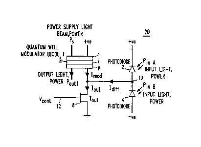
FIG. 1 illustrates one embodiment of the optical bipolar to unipolar converter
of the present invention. A bipolar optical signal comprises two unipolar
signals and
the power of the bipolar optical signal may be represented as the difference
in power
between two optical signals each defining one rail of the bipolar signal. In
FIG. 1 the
bipolar input signal is represented by optical beams PEA and P~ and thus the
value
20 of the bipolar signal is equal to the power difference (PEA - PCB). The
converter 20
includes two photodetectors 2 and 4 coupled in series. In the embodiment of
the
invention shown in FIG. 1 the photodetectors 2 and 4 are reversed biased
photodiodes.
A node 10 located between the photodiodes 2 and 4 is connected to an electro-
4
absorption modulator 6 and the drain of an output transistor 8. The electro-
absorption
modulator 6 generates a photocurrent that is proportional to the power of an
optical
beam incident thereon. The source of the output transistor 8 is coupled to
ground and
the gate of the transistor 8 is coupled to a constant voltage source 12. While
the
embodiment of the invention shown in FIG. 1 incorporates a field-effect
transistor
(FET), one of ordinary skill in the art will recognize that bipolar
transistors may be
employed instead. However, for the sake of clarity the following discussion
will
describe the invention as employing a FET.
In operation, the optical input beams P~ and Puig are incident upon
1o respective ones of the photodiodes 2 and 4. Because the photodiodes are
reverse-
biased, they each generate a photocurrent. As is well-known, the current
generated by
a typical reverse-biased photodiode is linearly proportional to the input
optical power.
For many photodiodes the proportionality between the current and input power
is such
that for every incident photon one electron of current is generated, i.e.,
IPC - ~ P~~ ( 1 )
where Ipc is the current generated by the photodiode, ~w is the incident
photon energy
and a is the electronic charge. For the sake of clarity the following
discussion will
assume that the converter of the present invention employs photodiodes
possessing this
characteristic. However, one of ordinary skill in the art will recognize that
the present
2o invention may employ instead photodiodes having a different relationship
between the
incident power and the generated photocurrent. Nevertheless, regardless of the
particular power-current relationship of the photodiodes employed, the net
photocurrent I~ff flowing out of the node 10 is proportional to the power
difference
between the optical beams PEA and Pig incident upon the photodiodes 2 and 4,
~5 respectively. Specifically, assuming that one electron is generated per
incident photon,
I~ff = e/~o,~(P~A - Puig)
The output FET 8 is biased so that the current Iout flowing through its drain
is
a function of the gate-source voltage and is substantially independent of the
source-
drain voltage. It is well-known that such ideal behavior may be obtained over
a given
operating range that varies from FET to FET. Accordingly, if the gate-source
voltage
of the output FET 8 is maintained at a constant value as indicated by the
arrangement
in FIG. 1, Imp will depend only on the currents I~ff and Iout~ where Imp is
the
current generated by the electro-absorption modulator 6. More particularly, by
conservation of current
1o Imod ~ lout - Idiff
It is well-known that certain electro-absorption modulators generate one
electron of photocurrent for every photon absorbed from the incident optical
power
beam. For such a modulator, the photocurrent Imp is proportional to the
optical
power absorbed in the modulator 6. This mode of operation is known as the
"self-
linearized modulator" mode and a modulator operating in this mode is referred
to as a
self linearized modulator. An example of a self linearized modulator that may
be
employed in the present invention is disclosed in the reference by D.A.B.
Miller et al.,
IEEE Journal of CZuantum Electronics, Vol. QE-21, Number 9, September 1985,
pages
1462-1476. While the electro-absorption modulators shown in FIG. 1 transmits
light
2o therethrough, other modulators may be employed in which the modulator
contains a
reflective surface for reflecting light back through the modulator. Moreover,
other
electro-absorption modulator having a self-linearized mode of operation may be
employed such as, for example, a bulk semiconductor diode that utilizes the
Franz-
Keldysh effect. Additionally, while the present invention will be described
below as
employing a self-linearized modulator, one of ordinary skill in the art will
recognize that
21~~~1~~
6
any electro-absorption modulator may be used for which the generated
photocurrent is
proportional to the absorbed optical power.
As seen in FIG. I, the modulator 6 is powered by an optical supply beam Ps
that generates the photocurrent Imp. The modulator 6 emits an optical output
beam
Pout that is smaller than the optical supply beam Ps due to the photons
absorbed to
generate the photocurrent Imp. If the modulator 6 operates in the self-
linearized
mode, the output beam Pout is smaller than the supply beam Ps by an amount
corresponding to one photon for every electron of current generated by the
modulator,
i.e.,
to Pout = Ps - (~c~Ye)Imod (4)
Eliminating Imp by substituting equation 3 into equation 4 yields:
Po~~ _ Ps - ~tc~ (Io~~ - Id~rr) (5)
a
Finally, substituting equation 2 into equation 5 provides a relationship
between the
output beam Pout and the difference between input signals PEA and Pte:
Po~~ _ (P~".4 - P~na) + Ps~ - ~w Io~~ (6)
a
Accordingly, the power of the output beam Pout is proportional to the input
2o power difference (PiI.~A - Pte) of the bipolar input signal, offset by an
amount linearly
dependent on the current Iout flowing through the drain of the output FET 8.
It should
be noted that if the term Iout were not present in equation (6) the converter
20 could
not convert an input signal for which Pip was greater than Pig because such a
CA 02145913 1998-07-09
7
situation would require that the output beam power Pout be greater than the
supply
beam PS, which is not possible because the modulator 6 is not a source of
optical
energy. In fact, if the term in equation 6 containing Iout were not present
the
modulator would not operate in its self linearized mode whenever PEA was
greater
s than Puig.
FIG. 2 shows a converter array that includes two converters 20 and 30 in
accordance with the present invention. While the converter array shown in FIG.
2-
includes only two converters, one of ordinary skill in the art will recognize
that the
array may include as many converters as desired for a particular application.
As
1o indicated in FIG. 2, the converters all may be powered by the same control
voltage
source 12 supplied to the gate of each transistor. One advantage achieved by
employing a single control voltage is that if the output transistors employed
in each
converter are substantially the same, then each converter will provide the
same linear
offset to the bipolar signal when it is converted to a unipolar signal since
the values of
15 lout for all the output transistors will be the same (see equation 6).
In an alternative embodiment of the invention the control voltage source 12
may be replaced by a control transistor 14 such as shown in FIG. 3, which is
powered
by an input current. The gate of the control transistor 14 is coupled to the
gate of each
output transistor of each individual converter employed in the array. The
control
2o transistor 14 is arranged so that it forms a current mirror with each of
the output
transistors. Current mirrors are well-known and serve to reproduce a current
from one
location to one or more other locations.
FIGS. 4-5 show examples of current mirrors that employ bipolar transistors and
enhancement-mode FETS, respectively. Examples of various current mirrors are
25 disclosed in U.S. Patent Nos. 5,134,358, 5,166,553 and 4,896,121.
CA 02145913 1998-07-09
g
Regardless of the type of transistor employed, each current mirror shown in
FIGS. 4-5 has an input transistor T;" and an output transistor Tot whose gates
(or bases in the case of the bipolar transistors shown in FIG. 4) are coupled
together.
The sources (or emitters) of the input and output transistors T;n and Tot are
also
coupled together and n the exemplary current mirrors shown in the figures the
sources (or emitters) are connected to ground. The drain (or collector) of the
input
transistor T;~ is coupled to the gate (or base) of both the input and output _
transistors T;" and Tot. In operation, a current I;" supplied to the drain (or
collector) of the input transistor T;" will be reproduced at the drain (or
collector) of
the output transistor To",. If the input and output transistors are not
identical, the
input current I;~ will be proportional to the output current Ia"t with non-
unity gain. In
FIG. 3, the control transistor 14 forms the input transistor of the current
mirrors and
the output transistors of each converter in the array form the corresponding
output
transistors of the respective current mirrors.
1 S The control transistor 14 allows the output current Io"t of each converter
to
be controlled by a single input current I;" supplied to the converter array.
As
a result, the value of the input current determines the value of the offset
applied
to the bipolar signal when it is converted to a unipolar signal. This
arrangement
may be advantageous over the arrangement in FIG. 2, in which the control
voltage
determines the value of the offset, because the offset is linearly
proportional to
the input current supplied to the control transistor ,14. In contrast, if a
control
voltage is used, the offset generally will not be linearly proportional to the
control voltage. This nonlinear relationship occurs
9~1~~~1~
because the source-gate (or emitter-base) voltage of a transistor is not in
general
linearly proportional to the source-drain (or emitter-collector) current.
Another
advantage achieved by using an input current to control the converter array
rather than
a control voltage is that the characteristics of a current mirror are
relatively insensitive
to temperature changes whereas a single transistor is significantly
temperature
dependent. In the case of bipolar transistors particularly, the relationship
between the
emitter-collector current and the emitter-base voltage is very temperature
dependent.
The converter and converter array of the present invention may be fabricated
from discrete components or as a single component monolithically integrated on
a
semiconductor wafer. Monolithic integration employing enhancement-mode FETs
may
be achieved by using conventional GaAs fabrication technology such as
described in
S.M. Sze, Physics of Semiconductor Devices, Wiley, New York, 2nd ed. 1981, p.
322.
Monolithic integration employing depletion-mode FETs, quantum well modulators,
and
photodetectors may be achieved, for example, by a method disclosed in L.A.
D'Araro
et al., IEEE Journal of (Zuantum Electronics, Vol. 29, Number 2, February
1993, pages
670-677.