Note: Descriptions are shown in the official language in which they were submitted.
~ 1 4~369
_
Microwave Apparatus For Depositing Thin Films
FIELD OF THE INVENTION
This invention relates generally to apparatus for sustaining a substantially
uniform microwave initiated plasma over a relatively large area and more particularly
5 to novel apparatus for the simultaneous microwave initi~ted glow discharge chemical
vapor deposition of uniform layers of thin film material over a plurality of large area
zones on an elongated web of microwave tr~n.~mi~.sive substrate material. The
microwave deposition assembly includes a linear, elongated applicator adapted to either
radiate or transmit microwave energy via evanescent waves into the interior of an
10 enclosure m~int~in~-l at sub-atmospheric pressure. In the most preferred embodiment,
the thin film material deposited upon the deposition surface of the web of substrate
material is an ultra-thin, transparent barrier layer for inhibiting the diffusion of oxygen
therethrough. Specific processing parameters are enumerated herein.
BACKGROUND OF THE INVENTION
One application of microwave energy is to efficiently create activated species
from gaseous precursors for use in plasma treatment processes, such as semiconductor
etching and thin film deposition. Previous microwave plasma deposition techniques,
which illustrate the state of the art and highlight both the problems encountered in
increasing the energy uniformity and the advantages provided by the microwave plasma
20 generating structure and thin film deposition apparatus of the instant invention, will be
discussed in the following paragraphs.
Commonly assigned, U.S. Patent Nos. 4,517,223 and 4,504,518 to
Ovshinsky. et al., both entitled "METHOD OF MAKING AMORPHOUS
SEMICONDUCTOR ALLOYS AND DEVICES USING MICROWAVE ENERGY"
~5 describe processes for the deposition of thin films onto small area substrates in a low
pressure, microwave glow discharge plasma. As specifically noted in these Ovshinskv
et al. patents, operation in the disclosed low pressure regimes not only elimin~tes
powder and polymeric formations in the plasma, but also provides the most economic
mode of plasma deposition. While these patents describe the revolutionary concept of
30 operating at low pressure and high energy density utili7ing microwave energy, i.e.,
operating at the substantial minimllm of the modified Paschen curve, the problem of
uniformity of the deposition of thin films over large areas remained addressed.
2 ~ ~ 4~3~ i
Turning now to microwave applicators for large area substrates, commonly
assigned U.S. Patent No. 4,729,341 of Fournier, et al. for "METHOD AND
APPARATUS FOR MAKING ELECTROPHOTOGRAPHIC DEVICES" describes a
5 low pressure microwave initi~te~l plasma process for depositing a photoconductive
semiconductor thin film on a large area cylindrical substrate using a pair of radiative
waveguide applicators in a high power process. However, the principles of large area
deposition described therein are limited to cylindrically shaped substrates, such as
electrophotographic photoreceptors, and the teachings provided therein are not directly
10 transferable to elongated, generally planar substrates.
While workers in the field have disclosed methods of processing thin films
lltili7in~ the high power of microwave sustained plasmas, previously microwave plasma
treatments have not been altogether applopliate for large surface area and/or low
pressure deposition. This is because of the non-uniformity of the plasma over an15 enlarged or elongated substrate due to the non-uniformity of the energy initi~ting the
plasma. One attempt to provide greater large area uniformity was the use of a slow
wave microwave structure. A problem that is inherent in slow wave structures,
however is the very rapid decline of microwave coupling into the plasma as a function
of distance transverse to the microwave applicator. This problem has been addressed
20 in the prior art by various structures that vary the spacing of the slow wave structure
from the substrate to be processed. In this way the energy density at the surface of the
substrate can be kept constant along the direction of movement of the substrate. For
example, U.S. Patent No. 3,814,983 to Weissfloch et al. for "APPARATUS AND
METHOD FOR PLASMA GENERATION AND MATERIAL TREATMENT WITH
25 ELECTROMAGNETIC RADIATION" and U.S. Patent No. 4,521,717 to Kieser et al.
for "APPARATUS FOR PRODUCING A MICROWAVE PLASMA FOR THE
TREATMENT OF SUBSTRATE IN PARTICULAR FOR THE PLASMA
POLYMERIZATION OF MONITORS THEREON", both address this problem by
proposing various spatial relationships between the microwave applicator and the30 substrate to be processed. More particularly"Weissfloch et al. discloses that in order
to obtain the uniform electric field intensity necessary for a plasma of uniform power
density along the full
_~0 94/11544 2 I 4 6 3 pcr/us93/1o841
structure at an angle with respect to the substrate. It should be app6l~:nt, however, that
inclinAtion of the slow wave waveguide structure with respect to the substrate, to achieve
~mirollllity, leads to an inefficient coupling of microwave energy into the plasma.
Recognizing this ~ficiPnçy, Kieser. et al. described that the c- n-lition~ resulting
5 from ~upel~osing of two energy inputs, i.e., two microwave applicators, can be further
improved if the two slow wave applicators are set at an angle to each other such that the
planes norrnal to the mP~iAn~ of the applicators intersect at a straight line which extends
parallel to the surfaces of the substrate to be treated and at right angles to the direction
of travel of the substrate. M~ er, Kieser. et al. I~co...l.~f~ e~ that in order to avoid
de;,~ clive int~,.rcl~ncc of the wave field p~t~.l.s of the two applicators, the applicators
should be displaced from each other transversely of the direction of travel of the substrate
by a ~istAn~e equal to half of the space between the cross-bars of the waveguide. In this
way the miclo~vavc field pattern is substAntiAlly s.-pplessed.
The l,lu~lenl of plasma unirollnily and more particularly, energy unifollllily was
treated by J. ~m~lssen and his co-wull~e.~, for example in T. Roppel, et al. "LOW
TEMPERATURE OXIDATION OF SlLICON USING A MICROWAVE PLASMA DISC
SOUROE", J. Vac. Sci. Tech. B-4 (J_nuary-rcb, ~ 1986) pp. 295-298 and M. DAhimPne
and J. Asmussen "THE PERFORMANOE OF M~CROWAVE ION SOUROE IMMERSED
IN A MULTICUSP STATIC MAGNETIC PELD" J. Vac. Sci. Tech. B-4 (January-
r*blualy 1986) pp. 126-130. In these, as well as other papers, Asmussen and his co-
WW~ described a miclowa~e reactor which they refer to as a ~I~icl~wdve plasma disc
source ("MPDS"). The plasma is lepol~,d to be in the shape of a disc or tablet, with a
diameter that is a function of micluwa~G frequency. A critical &dval,lage claimed by
Asll"lssen and his c~workers is that the plasma disc source is scalable with rl~uen~
that is, at the normal microwave frequency of 2.45 gigahertz, the plasma disc diameter
is 10 cçn~ cters and the plasma disc thir~nes~ is 1.5 cent;.~.~ter~, but that the disc
diameter can be inclGased by re~lçing the microwave frequency. In this way, the plasma
geometry was said to be sc~l~ble to large diameters, potentially yielding a Uni['Ollll plasma
density over a large surface area. However, ~smussen, et al. only desc~ibed a microwave
plasma disc source which is operational at 2.45 gigahertz, where the plasma confined
diameter is 10 centimeters and the plasma volume is 118 cubic centimeters. This remains
4 2~ 3~
_
far from being a large surface area. In order to provide for the deposition onto large
area substrates, Asmussen, et al. proposed a system operational at the lower frequency
of 915 megahertz, which would provide a plasma diameter of approximately 40
5 centimeters with a plasma volume of 2000 cubic centimeters. Furthermore, the
deposited material quality and deposition rate is dependent on excitation frequency. The
modulation of frequency to increase plasma dimensions comprises material quality and
film deposition rate.
Workers at Hitachi have described, for example in U. S . Patent No .
10 4,481,229 to Suzuki et al., the use of electron cyclotron resonance (ECR) to obtain a
high power plasma having a relatively high degree of uniformity over a limited surface
area. However, the Hitachi patent does not teach, nor even suggest a method by which
uniform large area plasmas may be achieved. Moreover, the use of ECR imposes theadded requirement of highly uniform m~gnPtic field structures in the microwave
15 apparatus, and may be restricted in operation to only those very low pressure regimes
where electron collision times are long enough to allow the ECR condition to be
achieved.
U.S. Patent Nos. 4,517,223 and 4,729,341 referred to above, describe the
necessity of using very low pressures in very high microwave power density plasmas
20 in order to obtain high deposition rates and/or high gas utilization. However, the
relationship between high deposition rates, high gas utilization, high power density, and
low pressure further limits the utility of slow wave structures and electron-cyclotron
resonance methods. The limitations of the slow wave structure and of the
electron-cyclotron resonance methods were obviated by the method and apparatus
25 disclosedincommonlyassignedU.S. PatentNo. 4,893,584, toDoehleretal., "LARGE
AREA MICROWAVE PLASMA APPARATUS".
However, the apparatus of the '584 patent, as well as the apparatus of the
prior art, each suffer from a specific inherent design problem. That is, the prior art
apparatus, due to their specific configuration, allow coating of the microwave ra~ ting
30 applicator isolating means (i.e. microwave window, protective cylinder, etc.) by the
deposition thereonto of material intended for the substrate web. In a continuous roll to
roll process, this coating of the isolating means can cause reduced microwave efficiency
5 2 ~ ~83~
-
at the intended deposition region, overheating of the isolating means and larger amounts
of "downtime" due to the necessity of cleaning or replacing the isolating means.It would be commercially advantageous to create a deposition apparatus in
5 which material could be deposited onto a continuous web of substrate material at
multiple sites upon the web during a single pass through the apparatus. This would
allow for higher overall web speed, and in the case of temperatures sensitive substrate
materials, would allow for multiple cooling stages between deposition sites to prevent
overheating and possible destruction of the web of substrate material.
One particular application for the deposition of thin film coatings onto an
elongated relatively wide web of substrate material is for the food packaging industry.
More particularly, there has recently arisen a desire to deposit thin film oxygen and
water vapor impermeable coatings atop an elongated polymeric web to be employed for
packaging and giving extended shelf life to perishable foodstuffs. In order to
15 accomplish this objective, researchers have previously developed thin film SiCO
coatings and have even suggested the significance of controlling the hydrogen content
of that thin film.
More particularly, the importance of controlling the hydrogen content of
prior art films for the purpose of, inter alia, depositing oxygen impermeable films has
20 been discussed in commonly assigned U.S. Patent No. 4,737,379. As was noted therein,
plasma deposited amorphous silicon hydrogen alloys, as well as alloys of silicon and hydrogen
with one or more of carbon, oxygen and nitrogen suffered from various shortcomings. The
hydrogen content was strongly dependent upon the substrate temperature, that content decreasing
at high temperatures and increasing at low temperatures. The deleterious effect of
25 hydrogenation on film properties, such as oxygen and water vapor permeability, is a direct
consequence of hydrogen's role as a chemical bond terminator. As such, hydrogen can disrupt
the connectivity of the chemical bond network of the deposited film, thereby reducing its
average atomic coordination number. The solution preferred by said '379 patent was to
eliminate the presence of hydrogen for the feedstock gases. This was at least partially due to
30 the fact that thermally sensitive substrates, such as plastics, could not be heated sufficiently to
eliminate hydrogen bonding in the deposited thin films. This inability to drive off hydrogen
produced thin films characterized by greatly deteriorated properties which limited the utility of
said films. However, the recipes set forth in the '379 patent fail to provide a film which
exhibits the type of oxygen and water vapor permeation
WO94/11544 2146369 PCI/US93/1~_
_ 6
characteristics d~m~nflecl by the food pack~ging industry.
Thelefcle, there is a need in the art for a continuous, roll to roll deposition
~)p~a~uS which substantially elimin~tss coating of the microwave ra~ ting applicator
isolating means by deposition material and allows for multiple simultaneous depositions
S upon a low l~lnpe-dlulc web of substrate material in a single pass through the ~)p~aluS.
There also exists a need for the deposition of thin film oxygen and water vapor
ilnp.,- .~-oahlP flexible co~tin~ atop a low telllpGlalule web of substrate material. These
and other needs are met by the micç~wave ~palalus and deposilion meth~ describedhereinbelow.
BRIEF SUMMARY OF THE rNVENIlON
There is di~rlose~l herein app~alus for the plasma enh~nr~ed chemir~l vapor
d~,~si~ion of thin film m~teri~l onto an elongat~ web of substrate m3tPri~ tili7ing a
linear microwave applicator. More specifir~lly, the a~p~ualus inrludes a d~,po~iL,on
chamber which is capable of being ev~ru~tP~l~ means for ev~u~ting the d~,po~i~ion
15 chamber to sub atmosphclic ~ Ul~;, and an elnng~ted web of substrate matP,ri~l disposed
in the dcpG~ilion chamber so that the dcposilion surface thereof substanti~lly enrloses a
first interior volume of the chamber. The volume enrlosed by the web of substrate
m~t~ri~l defines a first plasma region. The apparatus also inrlu(l~s means for intro1ucin~
a pl~ or mixture of d.,~o~ilion gases into the first plasma region, a first linear, non-
20 ev~l-escel-t applicator for the s~lbst~nti~lly uniçollll introclurtion of mi-,lowa~e energy from
a source into the first deposition region for dic~soci~ting the ~ or gas llliX , into
a plasma of activated species and depositing the mixture of activated species onto the
substrate. The linear applicator is operatively disposed adj~rent to the non-deposition
surface of the substrate. The ~l~;ul~or llliX~UlG of gases is subst~nti~lly col-r.,-ed by the
25 disposition of the web of substrate m~t~ri~l relative to the linear applicator, ~ "eby the
a~soci~ted pr~cul~ol llliXIul~ is subst~nti~lly prevented from depo~iling on the linear
applicator.
The ~alaLuS also inrlu-lP,s means for i~ol~ting the microwave radiating applicator
from the low pl~,s~ule deposition region. The ~l~lition~ ol~ting means is formed from
30 a material through which microwave energy can be radiated from the applicator means
into the vessel and is configured into a shape substantially optimized to withstand the
O 94/11544 21 ~ 63 6Y Pcr/US93/l084l
pressure differential to which it may be exposed. In this manner, the thir~nP.ss of the
isolating means may be minimi7~d and a substantially unifolm plasma operation may be
pelro"l,ed along the surface of the elong~tP~1 web of substrate m~tPri~1 disposed in the
deposition chamber. The i~ol~sing means is preferably cylindnc~lly or hemi-cylindrically
5 shaped so as to ell~A~ tç at least that portion of the applicator means which extends
into the vessel, though other generally smoothly curved surfaces may be employed with
equal success. A vacuum seal is disposed b~ ~n the cy1in-lri~11y shaped isolating
means and the vessel wall, so that a pl~.S:~Ulc dirr~ al may be m~inlAi~ bel~.~n the
interior and the exterior of the cylin-lrir~lly-shaped isolating means. Accordingly,
lO pressure (vacuum) m~inl~ini~g means is provided to m~int~in the ~l~s~u,e (vacuum) of
said vessel disposed eYterirJr1y of said cy1i~ ;c~11y-shaped isolating means at a p~GS:~UlC
apl,lv~;...~ting that l~u~d for plasma operation near the minimum of a modified
Paschen curve. The thirl~nçss of the cu~;ulllfelGn~ial wall of the i~ol~ting means is
designPcl to wi~ n-l that pl~,S~ , dirr~l~,ntial which exists ~,en the exterior and
15 interior thereof.
The applicator preferably takes the fo~n of an çlong~tP~ wa~eE,uide which in~ esat least one a~l ~u.~ for subst~nti~l1y ullirollllly r~i~tin~ mi~ wavt energy ~ ,Ll~ , into
the interior of the vacuum vessel. It is to be understood that the si~ of the ~ ulcs may
be periodic or ~pP,rio lir~ and the size of the a~ u,~ may be equal to or less t,han one
20 wavelength of the miclc~wà~ energy. In other emboflimPnt~, a plurality of apcllu,~s are
spacedly position~ along the 1onginldin~1 extent of the waveguide. Here, as above, the
size and sp~ing of the apellulGs may be either perio~ or ~pçliodi~
An el~ng~tçd ~ub~l.atG web is adapted to be co..l;..uQusly moved past the
]on~inldin~l extent of the waveguide. It is ~,lGfcll~,d that the substrate web is operatively
25 disposed within a near field distance of said applicator. The applicator is adapted to
s~1bst~nti~11y w~ llllly radiate mi~,lowave energy from the waveguide over a dimension
greater than one wavelength of the mic,~wa~,~,s and, preferably, greater than twelve
inches. The applicator may further include shutter means adapted to ensure that a
subst~nti~lly UllirOllll density of microwave energy is emitted from the apellul~, means
30 along the entire ]ongih1clin~1 extent thereof.
Thè ap~tus preferably further includes applicator cooling means. The cooling
WO 94/11544 21 4 6 3 6 9 PCI /US93/lC~_
means may be a flux of air adapted to flow about the interior of the isol~ting means. In
another preferred embodimPnt, the cooling means may include a concellL ic enclosure
formed interiorly of and shaped similarly to said i~ol~ting means so as to define a conduit
between said isol~ting means and said conce~lLlic enclosure. It is into this cond-1it that
5 a coolant fluid, examples of which include water, oils or freon, is adapted to flow.
The ability to utili~ thin i~ol~ting means insures that said isol~ting means can be
thermally cooled to a s-1fficiently low lenl~e;~LL~ that relatively high power miclu~ave
energy can be introduced into the vacuum vessel and excite a high electron density plasma
without the heat which is ~soci~tPfl tL~,~ith cracking said i~ol~ting means.
These and ûther objects and advantages of the instant invention will become
a~albllt from the Detailed Des~ ~ion, the Drawings and the Claims which follow
hereinafter.
BRIEF DESCRIPTION OF THE DRAWINGS
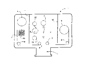
Fig. 1 is a schPm~tic cross s~ ;nn~1 view of a first embodiment of the del)osilion
15 al~palalus of the instant invention, spe~ifir~lly illu~llating the e~ f nl~ O~,a~ ,ly
oserl therein for ~.rr~ing the vn;ro~ micl~,..d~, plasma ~lepQsition on an e1nngPtP~
sub~llate; this figure iilu~llal~S an embol;...~nl of the instant invention having a single
plasma deposition region, employing a single gas manifold and a single e1rngatedmicrowave applicator;
Fig. 2 is a sçhPm~tir cross-sp-ction~l view of a second embolimP-nt of the
d~o~ilion a~zl~l~s of the instant invention, this embodilllent employing a single
dPpo~;l;on region, a single e1ong~tPJl micl~,~.d~,e applicator, and two gas manifolds, the
first of which is adapted to introduce the pre-cursor gase~,us Illi~lul~, and the second of
which is ~ pte-l to introduce a non-d~i~ing gas IlliAIUlC; to er~;lu&tt; plasma pre-
2~ l,.. er.t of the ~,posilion surface of the çlong~tP~ web of substrate m~tPri~l;
Fig. 3 is a schPm~tic cross-sp-ction~l view of a third embodhllellt of the deposition
al)pâlatus of the instant invention, this apl)dlalus employing two deposition regions, two
elongated mic~ a~/e applicators and two ~lecul~ol gas Illi~lule injection manifolds;
Fig. 4 is a schpm~tir cross-section~1 view of a fourth embodilllent of the deposition
30 a~tus of the present invention, this embodiment employing two elongated microwave
applicators and three gas manifolds, two of which are adapted to introduce precursor
~_ NO 94/11544 21 ~ 63 6 PCr/USs3/10841
gaseous llli~lWe into the deposition regions and a third adapted to introduce a non-
d~osi~ing gas mixture for the plasma pre-treatment of the deposition surface of the
elongated web of substrate m~teri~1;
Fig. 5 is a cross-sectional view of a portion of the apparatus of the instant
~ 5 invention, speci~lr~lly depicting a radiative linear microwave applicator unit opclillively
~rhp~d interiorly of the deposition chamber;
Fig. 6 is a fra~...e..l;~.y perspective view illustrating a first emb~liment of the
radiative microwave applicator of the instant invention with spacedly ~ pose~l discrete
urf s formed through one of the wider faces II,e~f,
Fig. 7 is a fragmPnt~ry pc,sp~li~e view illustrating a second emboflimpnt of theradiative mic,v..a.Je applicator of the instant invention with a single ç1ong~tPA ay~,.lwe
formed th~ough one of the wider faces thereof and shutter means ~i~posed ~ll~f~.~., and
Fig. 8 is a fr~...Pnti~y p~ .~;~ive view illu~ ~ing a second embo~ of the
linear radiative miclowd~ applicator of the instant invention in which the spacedly
15 disposed ~,.lur~s are formed along the 1Onpitn~lin~1 extent of one of the na,l.,.._r faces
thereof.
DETAILED DESCRIPI~ON OF THE INVENTION
The instant ul~,f n~ion relates to an ~ alus for the simullanc.,us plasma Pnh~n~e~l
chPmi~1 vapor depositic-n of thin film m~eri~l onto multiple portions of an e1Ongatçc
20 web of substrate m~teri~l ~lti~ ng a linear microwave applicator. Depositinn occurs
within an evac~tPd ~lf,po~;l;on chamber. By m~int~ining the vessel, at sub atmospheric
pl~s~ules, it is possible to opeMte the plasma at a p,es..u~e ~lv~ te1y that l~uir~d
for operation near the minimum of the modified Paschen curve. Low ~ .ul~, operation
also allows for a longer mean free path of travel for the plasma excited speciP s~ thereby
25 contributing to overall plasma ullifollllily. In tnis way, it is possible for the Illiclu~ave
deposition apparatus to sustain a urPiro~lll plasma reaction upon a substrate disposed witnin
the near field distance of the mi~;lowave source.
Fig. 1, illustrates, in schPm~tic cross-sfxtion, a first embalimçnt of a microwave
deposition app~u~lus 1 for ~ IA;~itlg a subst~nti~lly unirollll mi.;r~dve plasma over a
30 relatively wide web of substrate materiaL As used herein, the term "wide" refers to a
body having a wid~ di,nf nsion greater than one microwave wavelength, and preferably
WO 94/11544 2 1 4 6 3 6 ~ PCr/US93/10~_
greater than twelve inches. The apparatus 1 includes, inter alia, a vacuum vessel
deposition chamber 2, the walls of which are preferably formed of a durable, corrosion
resistant material such as stainless steel. The vacuum vessel deposition chamber 2 further
includes a pump-down port 3 adapted for suitable connection to a vacuum pump for5 maintaining the interior of the vacuum vessel deposition chamber 2 at an ap~.lo~u~iate sub-
atmospheric pressure. The vacuum pump is further adapted to remove reaction products
from the interior of said vessel 2.
The vessel 2 further includes at least one process gas input line connected to aprocess gas input manifold 9, which manifold 9 is operatively disposed so as to uniformly
10 distribute processed gases into the interior of said reaction vessel 2, and specifically into
the plasma deposition region 12 thereof. The process gas input manifold 9 is operatively
disposed b~ ..e~l- a pair of process gas c~ ,ent means 11 and between at least two
sections of the web of substrate material which define the deposition region 12. In
combination, the web of substrate material and the process gas containment means 11
15 contain the process gas introduced by the manifold 9 into the plasma region 12 of the
vacuum vessel deposition chamber 2.
During operation, the web of substrate material is drawn from payoff roll 5 and
guided by guide rollers 8 toward the deposition region. Guide rollers 8 may be variable
tension rollers to relieve stress upon the web of substrate material as it passes through the
20 deposition chamber. After passing along one or more guide roller 8, the web of substrate
material is passed between the linear microwave applicator 4 and the process gas injection
manifold 9. The web of substrate material is then passed around chill roller 7, again
passing gas port 9, around additional guide rollers 8, and collected upon take-up roll 6.
The sectinn~ of the web of substrate m~tçri~l extending between guide roller 8 and chill
25 roller 7 create an enclosed plasma deposition region 12. The precursor gas mixture
injected from gas manifold 9 interacts with the microwave energy supplied by theelongated microwave applicator 4 to create energized species in deposition region 12.
Deposition therefore occurs on both the section of substrate matçri~l leading toward and
moving away from chill roller 7. Because plasma deposition is inherently a high
30 temperature process, temperature sensitive substrates must be intermittently cooled so that
destluction thereof is avoided. This cooling is accomplished by chill roller 7. Cooling
~ ~O 94/11544 21 g 63 69 PCr/US93/10841
11
the web of substrate material allows for a longer overall exposure time to the plasma
deposition. The apparatus of Fig. l allows for high deposition rates and good process gas
utilization by allowing for deposition on at least two discrete portions of the web of
substrate material on a single pass.
The microwave deposition apparatus l further includes a microwave applicator unit
4 which extends at least partially into the interior of said vacuum vessel deposition
chamber 2. The microwave applicator unit 4 is adapted to radiate microwave energy from
a source thereof, into the interior of said vacuum vessel deposition chamber 2 for
initi~ting and m~int~ining a plasma of the process gases introduced into said vessel 2
through a process gas manifold 9. The specifics of the microwave applicator unit 4
inc1uding the microwave applicator and microwave applicator isolating means will be
discussed in detail hereinbelow.
Turning now to Fig. 2, there is shown a schem~tic cross-sectional view of a second
embodiment of the microwave deposition apparatus of the instant invention. This second
embodiment is similar to the microwave deposition apparatus of the first embodiment
(Fig. l) with the exception of the ~ ition of a deposition surface pretreatment zone. The
instant inventors have surprisingly found that microwave plellGalll,ellt of the deposition
surface of the web of substrate m~t~ri~1 enh~nces the barrier p~ Lies of the deposited
thin film. This microwave pre-tre~tmçnt is preferably a plasma pre-treatment and most
preferably an argon plasma pre-tre~tm~nt The argon plasma pre-treatment of the
deposition surface of the web of substrate m~teri~1 occurs in a plasma pre-treatment zone
13. The argon is injected into the plasma pre-treatment zone 13 by pre-treatment gas
manifold 14. The injected argon interacts with the microwaves from the linear microwave
applicator 4 thereby pretreating the deposition surface of the web of substrate m~teri~1
In order to pass the deposition surface of the web of substrate m~teri~1 past pre-treatment
zone 13, the guide rollers 8 on the payoff roll 5 side of the deposition apparatus l must
be moved to the opposite side of the microwave applicator vis a vis the deposition
apparatus of Fig. l. In addition, another roller lS must be added to the system. This
additional roller 15 can be either a guide roller or a quench roller as required. It is
hypothesized that this pretreatment process promotes the adherence of the coating to the
web and possibly even affects the growth kinetics thereof.
WO 94/l 1544 PCr/US93/10 _
~ ;-2146369 12
Turning now to Fig. 3, illustrated therein is a schematic cross-section of a third
embodiment of the microwave deposition apparatus of the instant invention. This third
embodiment is similar to the first embodiment of Fig. 1 except for the inclusion of an
additional deposition region 12 which includes an additional chill roller 7, an additional
5 gas manifold 9, an additional guide roller 8, and an additional linear microwave applicator
4. Also, the embodiment of Fig. 3 inchlclPs a microwave barrier 16 which reduces or
elimin~tçs the interaction of microwaves from the linear applicators 4. This embodiment
of the instant invention provides for very high deposition rates, due to the dual deposition
regions 12 which allow deposition on at least four discreet portions of the web of
10 substrate m~teri~l during a single pass. This higher deposition rate allows for faster
throughput of the web of substrate m~teri~l, for a given deposited thin f1lm thickness
This higher throughput speed reduces the lel.,pel~ture rise of the web of substrate material
at any given deposition zone by reducing the time of exposure to the deposition plasma
and allowing the web of substrate m~t~Pri~l to pass over cooling rollers between15 depositions.
Alternatively, the first deposition region of the microwave deposition appa,alus of
Fig. 3 may be used as a plasma pre-tre~tmPnt region. In this in~t~nçe, the deposition zone
12 which is closest to the pay off reel 5 would be used as a plasma pre-treatment zone
13, as in Fig. 2, by providing a non-depositing gas or gaseous mixture, such as argon, in
20 the first gas manifold 9. This ~ltçrn~tive embodiment would reduce any microwave losses
encountered by the deposition apparatus of Fig. 2 due to the plasma pre-treatment
microwave energy load by providing a separate linear microwave applicator for each of
the plasma pre-treatment and plasma deposition zones.
Turning now to Fig. 4, there is depicted therein a cross-sectional schematic
25 representation of a fourth embo~imPnt of the microwave deposition apparatus of the
instant invention. This embodiment combines both the dual deposition regions 12 of the
embodiment of Fig. 3 and the plasma pretre~tment region 13 of the embodiment of Fig.
2. Therefore, this embodiment allows for both high deposition rate/high throughput and
plasma pre-treatment of the deposition surface of the web of substrate material for
30 enhancement thereof.
As is illustrated in Fig. 5, the microwave applicator unit 4 comprises a
~VO 94/11544 ~ 1~B369 PCr/US93/10841
substantially rectangular waveguide 42 having an open end portion 44 at the terminal end
portion thereof extended into the vessel 2. The open end portion is adapted to avoid
standing waves. It is to be understood that the applicator unit 4 may alternatively be
sealed at the terminal end thereof. The waveguide means 42 includes a plurality of
5apertures formed through a wider face thereof. The apertures are dimensioned and spaced
to provide for the uniform radiation of microwave energy therefrom.
Illustrated in greater detail in Fig. 6, is a fragmentary perspective view of the
microwave applicator unit rectangular waveguide 42 having the terminal end portion 44,
and a plurality off spacedly disposed ap."lul~s~ 46, 48, 50, 52 and 54 formed through a
lOwider face thereof. As is illustrated therein, apertures 46 and 48 are blocked by
microwave absorbing material to prevent microwave energy from radiating therefrom. It
is to be understood that the density of the microwave energy radiated by the microwave
applicator waveguide 42 can be distributed in a desired, controllable manner simply by
blocking and partially unblocking various ones of the apertures. In Fig. 8, a second
15microwave applicator embotliment is depicted only differing from the Fig. 6 embo~liment
by the form~*on of said apelLu.~s through one of the nallo~. rectangular faces of the
waveguide. Experiment~ have demonstrated that it is possible to m~int~in plasma
uniformity over large area substrates, while increasing the amount of microwave energy
introduced into the chamber by forming the apertures in the narrow waveguide face. This
20is believed to be due to the fact that current nodes are convergent along the narrower face
as the microwaves travel through the rectangular waveguide structure.
The instant inventors have found that the size of the apellulcs is of great
signific~nce, in that the leak rate of microwaves through any one of said apertures is
strongly dependent upon the size of that ap.,llulG. While the size of the aperture may be
25either larger or smaller than a wavelength of microwave energy, in the embodiment of
Fig. 6, it is ~lefell~d that the a~llul~; be the size of, or smaller than one wavelength of
microwave energy. Additionally, the inventors have found that by partially unblocking
- the a~cllules, the apparatus l is capable of sustaining a plasma which is substantially
uniform.
30Referring now to Fig. 7, a third embodiment of the microwave applicator
waveguide 142 has an open end portion 144 thereof and a single elongated, rectangular
WO 94/1 1544 ' PCr/US93/1(~_
2I~ 6369 14
apellul~ 146, larger than a wavelength of microwave energy, formed through substantially
the entire length and width dimension of a wider face thereof. The open end portion is
adapted to avoid standing wave problems, though a sealed end portion may be employed
for a given application. The waveguide 142 allows microwave energy to radiate from the
5 entire apel~ulc 146, though without more, the concentration of microwave energy is
greatest at the end of the apellulc nearest the source of microwave energy. The
concentration of the microwave energy, and consequently the density of the plasma may
be regulated by employing at least one elongated either straight or slightly curved metallic
microwave shutter 150 operatively affixed to said microwave waveguide 142 by a single
connection 152 consisting of, for example, a pin 153 through a channel 155, on the side
of said waveguide nearest to the source of microwave energy. Disposed at the opposite
end of said elongated al cllul~ 146, and along the edges of said apellure, are dielectric
insulator blocks 154 f~bricatefl from, for example glass or teflon. The dielectric insul~tor
blocks 154 are adapted to form an in~ ting barrier bet~,en the waveguide 142 and the
microwave shutter 150. This is necess~ry since the miclow~ve shutter 150 may be
grounded to the waveguide means 142 only at the connection 152. ~d~lition~l contact
between the shutter 150 and the waveguide 142 will cause a so called "sizzling" ground,
i.e., an arcing contact.
The waveguide embodiments shown and discussed in detail in connection with
20 Figs. 6 and 7 are of the type generally known as "leaky" microwave structures in that
microwave energy is allowed to leak or radiate therefrom through a plurality of apel lures.
Alternatively, though not illustrated herein, the microwave applicators may be slow wave
microwave structures. The slow wave structure delivers a signific~nt part of microwave
energy by means of ev~n~scçnt waves. This type of slow wave structure was discussed
25 hereinabove with reference to the Weissfloch, et al. and Kieser~ et al. patents. The
microwave energy apparatus 1 of the instant invention substantially obviates theshortcomings inherent in slow wave structures, i.e., the rapid decline in applied energy
coupled to the plasma as a function of distance along the direction transverse to the
microwave structure. This shortcoming is subst~nti~lly obviated herein by, inter alia,
30 isolating the microwave applicator from the plasma region, thereby allowing the applicator
to sustain a more uniform plasma.
O 94/l l ~44 2 1 4 6 3 6 9 PCr/US93/10841
Returning now to Fig. 5, the microwave applicator unit 4 further comprises means60 for isolating the microwave waveguide 42 from the deposition chamber 2. The
isolating means 60 is preferably fabricated from a dielectric material which is substantially
transparent to microwave energy. A ~lcf~ ,d m~tPri~l from which said isolating means
5 60 may be fabricated is quartz, though it is to be understood than many other m~teri~ls
may be employed with equal success. The isolating means 60 should further be
configured in a shape designed to optimize its ability to withstand forces due to the
presence of a pressure differential. In this manner, the thicknçss of the isolating means
may be minimi7~d to provide for effective thermal cooling whereby high microwave10 power den~iti~s may be employed without deleteriously effecting the isolating means. To
this end, a ~lefell~,d shape for said isolating means is cylindrical or hemi-cylin(lric:3l as
to encapsulate at least that portion of the waveguide 42 which extends into the vacuum
vessel 2.
A cylindrical or hemi-cylindric~lly shape is ~lG~ d to for example a planar
15 shape, because a cylinder may be made thinner than a planar shape due to the strength
inherent in a cylinder. Thus, a thin cylinder is capable of withstanding pressures which
would require a much thicker planar plate. ~d-lition~lly, a thick plate cannot be
m~int~int-d at a u~liÇOll~., relatively low tel..pelalule, as can a thin cylinder. Thus, a planar
plate may be subject to therm~l degrad~tic n, in a microwave plasma apparatus particularly
at elevated power levels. By contrast, the thin cylindrical isolating means 60 may be
unifol.~ly cooled, and thus does not experience thermal degradation, and therefore does
not impose practical limit~tions upon the amount of power which may be applied.
~d-lition~lly, the waveguide 42 should be operatively disposed within the isolation
means 60 and spaced from the circumferential wall thereof. So disposed, the waveguide
42 may extend partially through the vacuum vessel 2, without being directly exposed of
the plasma regions 12 or 13 c~ nt~in~d therein.
The cylindrical isolating means 60 of Fig. 5 is configured so as to be coextensive
with at least one dimension of the vacuum vessel 2, and protrude through at least a first
and second wall portion of said vacuum vessel 2. The cylindrical isolating means 60 is
fixed through the walls of the vacuum vessel 2 by means of two collar fittings 62 and 64
which are preferably mutably joined to the stainless steel vessel 2. Collar fitting 62
WO 94/11544 21~ 6 3 6 9 PCr/US93/10~_
- 16
comprises an open end portion 66 extending from a connection flange 68 affixed directly
to a side wall of the vacuum vessel 2, and includes an opening 70 co-extensive with the
circumference of the cylindrical isolating means 60 and adapted to receive cylindrical
isolating means 60. Open end portion 66 extends from said connection flange 68, and is
adapted to receive at least two O-rings 72, 74, which O-rings 72, 74 are adapted to effect
a vacuum and water barrier between the interior of said vacuum vessel 2 and outside
ambient conditions. Between O-rings 72, 74 is disposed a cooling channel 73 through
which a cooIing medium such as water may be circulated to m~int~in the O-rings at a
unifornly low tell-peldture. The O-rings 72, 74 are preferably adapted to m~int~in the
vacuum and water seal at substantially elevated l~lllpeldtulcs, i.e., tempeld~ures in excess
of 100~ Centigrade.
The cylindrical isolating means 60 passes through opening 70, connection flange
68, and the open end portion 66. In this way, O-rings 72, 74 are urged against the outside
circumference of said cylinrlric~l isolating means 60. The compression of the O-rings 72,
74 against the cylinrlric~l isolating means 60 results in an air tight, water tight seal. It is
hll~ulL~lt to note that the loc~tion of O-rings 72, 74 is well outside the plasma region 12
of the ~ us 1. This is notewolLhy because by keeping the O-rings out of the plasma
region 12, they are not exposed to the excessive ~elllp~,~tures associated with microwave
plasmas, i.e., lellll)~dLules in excess of 500~ Centigrade. Had the O-ring seals been
located within the plasma region, as shown in the aforementioned U.S. Patent No.4,729,341, special (and costly) high telll~ ture resistant seals would have been required,
greatly increasing the complexity and cost of the apparatus 1.
The cylindrical isolating means 60 may extend beyond the outside terminal edge
of said open end portion 66. This portion of the cylin~lric~l isolating means 60 must thus
be equipped with microwave cont~inment means 80. The microwave containment means80 is typically fabricated from a metal microwave containment canister operatively affixed
around the outside circumference of the cylindrical isolating means 60, and in electrical
contact with said open end portion 66 by grounding fingers 82. The microwave
cont~inment canister is fabricated so as to be coextensive with that portion of cylindrical
isolating means 60 which extends beyond the open end portion 66. Additionally, the
microwave cont~inment means 80 further includes an open end portion 84 over which is
~_~O 94/11544 2 1 4 6 3 6 9 PCr/US93/10841
17
disposed a metallic microwave blocking mesh 86 adapted to contain stray microwaves
thel~wil}~ . The mesh 86 is also adapted to allow for the passage of a flux of cooling
air through the cylindrical isolating means 60. ~ltrrn~tively, and as is illustrated in
phantom in Fig. 5, the opened end portion 84 of the microwave con~ ent c~ni~trr 80
S may be ~tt~hecl to a dummy load adapted to absorb excess microwave r~ tion This
embodiment is particularly useful at high power levels, where excess refl~cted ~ wa~e
energy causes reflection modes which may degrade the ullir~Jllllily of the microwave
pl~mQ .
The vacuum vessel 2 is further adapted to receive the cylin-lric~l i~ol~ting means
60 through at least a second wall portion thereof, preferably the wall portion opposite the
wall portion upon which collar fltting 62 is mounted. Collar fitting 64 is disposed on said
opposite wall position, subst~nti~lly in line with collar fitting 62. Collar fitting 64
comprises an open end portion 90 çxtrn(lçd from a comlPclion flange 92. Cbnnection
flange 92 is affixed dil~lly to the o~p~ssile wall position and incllldes an opening 94 co-
e~lensi~e with the cil~ulllçel~nce of the cylin-lric~ ol~ting means 60. The open end
portion 90 extends from the conllP,~-I;on flange 92, and is adapted to receive at least two
O-rings 96, 98 which are adapted to effect a vacuum and water barrier ~I~.~n thevacuum vessel 2 and the ~ Junding ambient condition~ Between O-rings 96, 98 is
disposed a cooling ch~nnçl 97, through which a cooling m~ m such as water may becirculated so as to m~int~in the O-rings at a ullirollllly low ~e~llp~la~ e. The O-rings 96,
98 like O-rings 72, 74 are adapted to with~t~n(l elevated ~Inp~"dlu~s. The cylindrical
isolating means 60 is passed through opening 94, through connPction flange 92 and open
end portion 90 whereby O-rings 96, 98 are urged against the outside circumferential edge
of said cylindrical i~ol~ting means 60. The colllpl~ssion of said O-rings is the merh~ni~m
by which an air tight. water tight seal is effçcted Also, O-rings 96, 98, like O-rings 72,
74, are well out of the plasma region 20, and IL~,~îole not subjected to degradation
thereby.
By effecting an air-tight, water tight seal around the outer circumference of the
cylin(lrir~l isolating means 60, it is possible to m~int~in the vacuum vessel 2 at
subst~nti~lly sub-atmospheric pressures, while the interior of the cylintlric~lly isolating
means 60 is m~int~ined at atmospheric ~l~SSU~S, and is directly exposed to ambient
WO 94/1 l544 21 4 ~ 3 6 9 PCr/US93/10_
18
conditions. This is in fact an advantage in the operation of the ~ us 1. By
maintAining the vacuum vessel at sub-atmospheric pressures, it is possible to operate the
a~par~lus 1 at a pressure approximating that required for operation near the minimum of
a modified Paschen curve. Additionally, the low pressures allow for a longer mean free
5 path of travel for the plasma species, thereby contributing to overall plasma uniro~ y.
Since the interior of the cylin-lric~l isolating means 60 is exposed to ambient con(litions,
a flux of cooling air may be mAint~in~ thclcLhlough so as to prevent the excessive
heating which may be associated with micluwavG plasmas. ~ ...A~;vely, a microwave
trAn~mi~sive cooling medium such as silicon oil may be circulated within the cylinder to
10 mAintAin a u~ Ollll, cool LclllpCl~ulc. The cylintlricAl isolating means 60, extending
beyond the open end portion 90 must be ~hP~thed within a m~tAlli~ microwave
conlAi~ ent means 100, of the type described hereinabove. The micluw~vG cclnlA;~-...f.-t
means 100 is disposed adjacent to con--ecl;rn plate 102 which affects a co~-ne~;l;Qn
between the miwuwave waveguide 42, and a source of micruwavc energy.
Another form of substrate ~lcLle~ --t'nt, which may be used with or without plasma
et~ t...ent, is a th~rm~l bake-out of the substrate material. This bake-out may be
~cco.--~lished by providing a heat ~ ne~ator (i.e. coil, lamp etc.) in the a~al~Lus such that
the substrate passes nearby before any plasma plel~G~ ..t or deposition occurs. See, for
example, heater 300 in Fig. 1. This bake-out of the substrate is thought to drive off water
from the buLk of the substrate, thereby reducing the water vapor tr~n~mi~sion rate of the
coated product.
Finally, although enclosure of the deposition plasma region 12 within the folds of
the web of substrate material 10 is highly effective in preventing the deposition of coating
m~teri~l onto the quartz isolation tube, a web of miw~wave tran~mi~sive material on pay-
out roller 200 (Fig. 1) may be operatively positioned interiorly of said d4po~ilion chamber
1 so as to slowly move about the surface of the isolation means of the linear microwave
applicator 4 and be wound about the take-up roller 201. When the microwave
tr~n~mi~sive web is coated with an excess thickness of depositing barrier m~t~riAl, the
rollers are indexed and a clean portion of the web is allowed to collect the unwanted
buildup. In this manner, even at extremely high rates of deposition, no coating is
deposited onto the outer surface of the isolation means (the quartz tube). Accordingly,
_~0 94/1 1544 ~ PCI /US93/10841
~l~6369
19
the deposition process can proceed for long periods of time and is specifically adapted for
volume production.
EXAMPLE 1
A microwave deposition apparatus 1 as described hereinabove with reference to
- 5 Fig. 1 was employed to f~brir~te a clear silicon based thin film oxygen permeation barrier
layer coating upon an elongated web of polyester substrate material. The exact steps by
which the above described ~p~Lus 1 was used to f~bric~te such coatings will be det~
hereinbelow.
An elong~t~d roll of 0.5 mil (12 micron) thick 30 cm wide polyester was used as
the substrate for the instant example. The roll of polyester substrate was loaded onto the
payout roller of ~p~a~uS 1 described hereinabove with reference to Fig. 1. After placing
the substrate onto the payout roller 5, the ~p~LuS 1 was closed and sealed so as to
effect an air tight seal between the interior of the vessel and the surrounding ambient
con-litiQns. The interior of the vessel was then evaru~t~ to a plei,~ulc of ~lv~ tely
20 to 25 millitorr. Thereafter, the interior of said chamber was purged in an argon gas
Cll~/ilOnlne,.)t for a period of a~plo~; .n~t~ly one-half hour. After purging for ~p~Ai...ately
one-half hour, the chamber was ev~c~tçd to a background ~lcssurc of applo~;."~tely 3
to 4 millitorr. Thereafter, plcfcllcd fee~stoc~ gases were introduced to the interior of said
chamber through said input gas manifold 9 according to the following recipe:
GAS FLOW RATE
SiH4 180 SCCM
CO2 500 SCCM
~2 500 SCCM
Ar 400 SCCM
A general range of gases for this four component mixture would be about 100
to 200 SCCM SiH4, 300-700 SCCM ~2~ 300-700 SCCM CO2 and 300-700 SCCM Ar.
After initi~ting the flow of these feedstock gases into the interior of the vacuum
30 vessel, a microwave plasma was initi~ted at a frequency of 2.45 GHz and at a power of
a~lo~il"ately 5 kilowatts. The elong~ted web of substrate m~teri~l was passed through
WO 94/11544 214 6 3 6 9 PCr/US93/10~_
the deposition region 12 of the appaldlus 1 at a rate of about 20 m/min. During the
operation of the microwave plasma, a flux of cooling air was directed through the
cy1in-1ri~1 isolating means 60 so as to m~int~in a uniform low le~ dture. Thereafter,
microwave plasma was extinguished, and the flow of process gases to the vacuum vessel
5 2 was tormin~se~l
After extinguishing the plasma and termin~ting the flow of process gases to the
vacuum vessel 2, the interior of the reaction vessel was purged with argon, and the
reaction vessel was vented to ambient con(litinn~. Thereafter, the reaction vessel was
opened and the substrate was removed for e~min~sinn which revealed a uniform, clear,
l0 silicon based, thin film, oxygen permeation barrier coating on the web of substrate l0.
Tests in~ te that the dcposilcd film has the ch~omir~1 composition SiO,~, where
x=1.8-2. Oxygen p.,.llleation tests on a coated substrate having a 200 A thin film
deposited thereon show an ~2 perm~ti~ n of 1 cm3/m2/day at room Iclnpcldture and 0%
relative hllmi-lity.
In order to obtain the impressive oxygen and water vapor i-l.p~,~.. eability
behavior described herein, it was n~cess~ry to devise a method of elimin~ting hydrogen
from the deposited film taking into account the low melting point of the PET substrate.
In this regard, both the effect of increased oxygen concentration in the precursor gaseous
mixture was studied and the ch~mi~1 bonds responsible for water vapor diffusion were
20 studied by conducting IR spectroscopy on sample films deposited on crystalline silicon
wafers. Table A summ~ri7~s the relationship of Si-H concentration versus water vapor
tr~n~mi~sion and the precursor mixture.
A perusal of Table A will ~lemon~trate that the Si-H concentration and the
water vapor tr~ncmicsion decreases with the increase of oxygen concçnsration in the
25 precursor gaseous mixture. It is, of course, well established that Si-H bonds readily react
with water. Accordingly, it is not surprising that Si-H bonds in the deposited films will
absorb, react with and create a trancmi~sion pathway for the water vapor. The conclusion
to be drawn is that the relatively poor water vapor permeation ~ro~ ies shown insamples l and 2 were due to the presence of Si-H bonds in the films and that increased
30 oxygen concentration in the precursor mixture çlimin~te(l those Si-H bonds and increased
the impell--eability of the films. Note that the further increase of oxygen concentration
_~VO 94/11544 PCr/US93/10841
21 2 ~ 69
in the precursor beyond that indicated in Sample 3, failed to in~ uve the water barrier
plol)el ~ies. Of course, the plasma treatment process detailed hereinabove further improved
the balTier plv~elLies of the deposited film.
TABLE A
SAMPLE FEEDSTOCK Si-H H2O VAPOR
No. GASES BOND TRANS. RATE
(SCCM) CONTENT (gm/m2-24 hrs.)
SiH4 CO2 Ar ~2 38~C, 100% RH
220 750 450 275 0.5% 26
2 220 400 450 400 Trace 11
3 150 500 450 500 None 7
EXAMPLE 2
A microwave deposition al)p~dlus 1 as described hereinabove with reference
to Fig. 2 was employed to fabricate a second clear silicon based thin film oxygen
permeation ba~ier layer coating upon an elong~ted web of polyester substrate m~teri~l
A roll of 0.5 mil (12 micron) thick 30 cm wide polyester was again used as the substrate.
The roll of polyester substrate was loaded onto the payout roller of a~a,~lus 1 described
hereinabove with ,~fe,cnce to Fig. 2. After placing the substrate onto the payout roller
5, the a~ard~us 1 was closed and sealed so as to effect an air tight seal between the
interior of the vessel and the surrounding ambient cnn~litions. The interior of the vessel
was then evacuated to a pressure of applu~illlately 20 to 25 millitorr. Thereafter, the
interior of said chamber was purged in an argon gas envilol~ ent for a period ofap~oAilllately one-half hour. After purging for ~l~xi..,~tely one-half hour, the chamber
was evacuated to a background pressure of a~)p,u,.illlately 3 to 4 millitorr. Thereafter,
feedstock gases were introduced to the interior of said chamber through said input gas
30 manifold 9 according to the following recipe:
WO 94/11544 2 1 ~ 6 ~ 6 9 PCI/US93/10~_
22
GAS FLOW RATE
SiH4 300 SCCM
~2 900 SCCM
He 100 SCCM
A general range for this three component mixture would be about 200-400
SCCM SiH4, 800-1000 SCCM ~2~ and 0-200 SCCM He.
lition~lly, 400 SCCM of Ar was introduced to the plasma ylct~ nt zone
13 through gas manifold 14. After initi~ting the flow of these gases into the interior of
10 the vacuum vessel, microwave plasmas were initi~te~l at a frequency of 2.45 GHz and at
a power of ayylu~ ately 6 kilowatts for Ar plasma pretreatment and S kilowatts for
plasma deposition. The elongated web of substrate m~tt-ri~l was passed through t h e
plasma pretre~tment region 13 and deposition region 12 of the apparatus 1 at a rate of
about 20 m/min. During the operation of the microwave plasma, a flux of cooling air was
15 directed through the cylindrical isolating means 60 so as to m~int~in a uniform low
lelnp~ldlul~i. Th(,l~,drLcr, microwave plasma was extinguished, and the flow of process
gases to the vacuum vessel 2 was t~rmin~t~
After extinguishing the plasma and ~elllli~ g the flow of process gases to the
vacuum vessel 2, the interior of the reaction vessel was purged with argon, and the
20 reaction vessel was vented to ambient con-lition~. Thc.~ cr, the reaction vessel was
opened and the substrate was removed for e~min~sion which revealed a unifol~ll, clear,
silicon based, thin film, oxygen permeation barrier coating on the web of substrate 10.
Tests inrli~te that the deposited film has the chemiçal composition SiO", where
x=1.8-2. Perme~tion tests on a coated substrate having a 150 A thin film deposited
25 thereon show an ~2 tr~n~micsion rate of less than 1 cm3/m2/day at room telnyclaLure and
0% relative hnmi~lity and a water vapor tr~n~mi~sic-n rate of less than 1 g/m2/day at 38
~C and 100% relative h~lmi~lity.
While the specific examples of the method of depositing high barrier coatings
by microwave plasma enhanced CVD recited herein above are described with reference
30 to flat rolls of substrate m~teri~l and the apparatus of the instant invention, it should be
noted that the present method is useful for deposition of high barrier coating onto
2146369
.~0 94/11544 PCrtUS93/10841
substrates of any shape, by any machine which is capable of deposition onto the desired
substrate. Other types of substrates which would benefit from a coating of high barrier
material would be those such as plastic bottles, jars or other plastic containers in which
the m~teri~l to be stored is sensitive to water or oxygen. Of specific interest is coating
5 the interior of plastic bottles or jars for storage of food or beverages. As long as the basic
microwave deposition steps are present (i.e. such as th~ l bake-out, plasma
ell~,atlllent, microwave PECVD of high barrier coating etc.), the shape and/or si~ of the
substrate and/or portion of the substrate to be coated is irrelevant.
While the invention has been described in conn~ction with l~lef~ d
10 embodiments and procedures, it is to be understood that it is not intended to limit the
invention to the described embodim~nt~ and procedures. On the contrary it is intended
to cover all alternatives, modifications and equivalence which may be includecl within the
spirit and scope of the invention as defined by the claims appended hereinafter.