Note: Descriptions are shown in the official language in which they were submitted.
~'~~~~ 9~
FIELD OF THE INVENTION
This invention relates to current detectors,
and in particular to improved current detectors that can
be used as telephone system loop current detectors.
BACKGROUND TO THE INVENTION
Line current loop detectors in a telephone
system typically detect either a change of voltage
related to current flow change resulting from a
subscriber going off-hook or on-hook, or a change of
loop current flow in the line itself. A loop current
detector, to which the present invention is directed,
must be isolated from the loop or other line in which
current is to be detected. Typically an optocoupler is
used, in which a light emitting diode, optically coupled
to a photosensor, is driven by current derived from the
voltage difference established across a resistor (e. g.
100 ohms) connected in series with the line in which
current is to be detected, and through which the current
to be detected passes.
Current through the optocoupler diode is
limited by a typically 10 ohm series resistor. This
means that the optocoupler diode must reliably carry 100
ma. under some conditions. This severely limits the
choices of optocouplers that can be used.
Loop current detectors also sometimes cause
problems with line balance, and require optocouplers
containing light emitting diodes that are capable of
handling wide current ranges. Such diodes have been
found to be sensitive to secondary current surges. In
order to avoid early failure of the optocoupler, loop
currents must be limited to relatively low values, e.g.
less than 100 ma.
SUMMARY OF THE PRESENT INVENTION
In accordance with an embodiment of the
invention, a loop current detector circuit provides a
s
214 659 fi
robust diode based voltage source for powering an
optocoupler, in which there is substantial immunity to
surges, and which protects the optocoupler to a
substantial extent.
In accordance with another embodiment, a loop
current circuit utilizes a resistor for providing a
voltage source for powering an optocoupler in which the
resistor is extremely small, e.g. an order of magnitude
less than that required in the prior art, which reduces
the likelihood of problems caused by line imbalance
resulting from the presence of the resistor.
In accordance with another embodiment,
optocouplers are not required, while isolation and
longitudinal balance are maintained. Very high loop
currents can be handled, factory adjustments are
avoided, and the cost of the detector can be very low.
In accordance with an embodiment of the
invention, a current detector for connection in series
with a lead carrying current to be detected is comprised
of a first branch comprising a plurality of series
connected diodes having an anode end and a cathode end
for connection to said lead, a first optocoupler light
emitting diode connected in series with a resistor,
connected in parallel with the first branch, the
optocoupler diode being connected in the same polarity
direction as the diodes in the first branch, and a first
further diode connected in parallel with the first
branch, in opposite polarity direction as the diodes in
the first branch.
In accordance with another embodiment, a
current detector for connection in series with a lead
carrying current to be detected, is comprised of a first
branch comprising a plurality of series connected diodes
having an anode end and a cathode end, a first
optocoupler light emitting diode connected in series
2
214s~9s
with a resistor, connected in parallel with the first
branch, the optocoupler diode being connected in the
same polarity direction as the diodes in the first
branch, and a full wave rectifier circuit, having a pair
of terminals connected to the first branch, and another
pair of terminals for connection to said lead.
In accordance with another embodiment, a
current detector for connection in series with a lead
carrying current to be detected, is comprised of a first
resistor having a pair of terminals for connection to
the lead, an operational amplifier, a pair of resistors
connecting inputs of the amplifier to respective
opposite terminals of the first resistor, and a variably
tapped resistor connected between the inputs to the
amplifier with its tap to a reference source, and a
first optocoupler light emitting diode connected in
series with a resistor between an output of the
amplifier and the reference source.
In accordance with another embodiment, a current
detector for connection in series with a balanced pair
of leads carrying current to be detected, is comprised
of a pair of equal valued first resistors, each for
connection in series with one of the leads, two pairs of
similar antiparallel connected diodes, each pair being
connected in parallel with one of the first resistors, a
differential amplifier having inputs connected through
corresponding equal valued resistors to respective
opposite ends of one of the first resistors, a voltage
divider having a series connected pair of equal valued
resistors and a tap connected to a reference voltage
source, a pair of comparators, having noninverting
inputs both connected to an output of the differential
amplifier and inverting inputs respectively connected to
a voltage offset points offset in opposite directions
from the voltage source, and forward and reverse
3
~1~~6~~~
detected current output leads connected to respective
outputs of the comparators.
BRIEF INTRODUCTION TO THE DRAWINGS
A better understanding of the invention will be
obtained by reading the description of the invention
below, with reference to the following drawings, in
which:
Figure 1 is a schematic diagram of an
embodiment of the invention,
Figures 2 and 3 are schematic diagrams of
variations of the embodiment of Figure 1,
Figure 4 is a schematic diagram of an
embodiment of the invention,
Figures 5 and 6 are schematic diagrams of
variations of the optocoupler circuit portion of the
embodiment of Figure 4,
Figure 7 is a schematic diagram of an
embodiment of the invention which does not require the
use of optocouplers.
DETAILED DESCRIPTION OF THE INVENTION
Various embodiments of the invention will be
described with the application of sensing subscriber
loop current in a telephone system. However, it should
be recognized that this invention is applicable to, and
is intended also to be used in current sensing
applications in the consumer, automotive and/or
commercial control fields, including the replacement of
current operated relays in, for example, industrial
alarms.
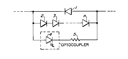
A first embodiment of the invention is shown in
Figure 1. A circuit such as that shown is inserted in
series with either the tip or ring line of a subscriber
loop. Diode 1 is connected in series with the line in
the reverse biased direction relative to the subscriber
loop voltage, and diodes 2, 3 ... n are series
4
connected, in parallel with diode 1, in the forward
biased direction. An optocoupler light emitting diode 4
(coupled to a photosensitive element, not shown) is
connected in series with a current limiting resistor 5,
in parallel with and in the same conductivity direction
as the diodes 2 - n.
Diode 1 provides a low voltage drop conduction
path in the reverse conducting direction around diodes 2
- n. The latter, in series, create a voltage drop
sufficient to cause the optocoupler diode 4 to operate.
Thus diode 1 limits the peak inverse voltage rating
needed by the optocoupler 4 to the maximum forward
conducting voltage drop of diode 1.
Similarly, diode 1 need have no higher peak
inverse voltage rating than the sum of the forward
conducting voltage drops of diodes 2 - n.
In operation, diodes 2 - n are forward biased,
and have a voltage across them falling in the range of
the minimum forward conducting voltages of optocoupler 4
plus the IR drop across resistor 5 to the sum of the
maximum forward conducting voltages of diodes 2 - n. It
has been found that this voltage range is much smaller
than that obtainable using a simple voltage dropping
resistor, as in the prior art. The reliability of
sensing an off-hook condition, or other loop current
conditions, by means of an optocoupler, is thus
significantly enhanced.
Figure 2 illustrates a variation of the above-
described embodiment. In this case, diode 1 is not
used, but in its place series connected diodes 6, 7 ...
m are used. The peak inverse voltage of diode 1 is thus
increased to the total of diodes 6 - m. Two optocoupler
diodes 4 and 9 are illustrated, connected in
antiparallel, the antiparallel diodes in series with
resistor 5. In this case the circuit can detect current
5
flow in either direction by means of the respective
optocoupler diodes 4 and 9.
Indeed, in the latter case, only a single
string of diodes 2 - n or 6 - m need be used if reverse
current is not to be expected and if line balance is not
important, the appropriate optocoupler diode voltage
being developed in the forward biased direction across
the remaining series of diodes.
It should be noted that in place of a series
string of diode 6-m, a full wave diode bridge may be
used, as shown in Figure 3.
Typical of all of these cases is the case shown
in Figure 2 where the current to be detected is divided
between either the diode string 2-n and
optocoupler/resistor 4, 5, or the diode string 6-m and
optocoupler/resistor 4, 5.
In some cases, optocoupler light emitting
diodes are incapable of handling wide current ranges
experienced on the line. Figure 4 illustrates another
embodiment of the invention, which substantially
eliminates this problem (as in the above embodiments,
one circuit as described being inserted in series with
each lead of a balanced line, if desired).
A small resistor 15 is connected in series with
the lead in which current is to be detected, across
which a voltage is developed. A pair of resistors 16
and 17 are connected to respective ends of resistor 15,
and in series with a variably tapped resistor 18 such as
a potentiometer, the tap of which is connected to
ground. An operational amplifier 20 having resistor 21
connected between its output and its inverting input,
has its inputs connected across resistor 18. The output
of operational amplifier 21 is connected to an
optocoupler light emitting diode 23 which is connected
in series with a current limiting resistor 25 to ground.
6
2146596
Another optocoupler diode 27 may be connected in the
reverse polarity direction to diode 25, in parallel with
diode 23.
In operation, current in the lead develops a
voltage across resistor 15. This voltage is detected in
operational amplifier 20, which in response applies
current through either of optocoupler diodes 23 or 27,
depending on the direction of current flow in the
resistor 15 and the resulting direction of current flow
out of amplifier 20.
Two important aspects of this embodiment are
that the voltage developed across resistor 15,
corresponding to the current to be detected, is
amplified by the operational amplifier 20, which
provides an indication of the on or off hook condition
with less chance of line balance problems than prior art
circuits. Due to the existence of the amplifier, the
resistor 15 can be smaller value than in the prior art,
requiring less voltage to be developed across it for
detection, thus providing less imbalance. The imbalance
results from inexact resistances of corresponding
resistors in a pair of balanced leads, or less
resistance added to the line in the case of a single
unbalanced lead (and also in the case of a pair of
balanced leads).
For example, if the forward voltage of the
optocoupler light emitting diode is 1.4 volts, the gain
of the amplifier is 100, the signal voltage across
resistor 15 is 14 mv., the minimum loop current to be
detected is 16 ma., the resistor 15 need only be 0.875
ohm, which is an order of magnitude less than is
typically used for such an application.
Another important aspect of the present
embodiment is the use of variably tapped resistor 18,
which facilitates zero setting of the operational
7
214659fi
amplifier. In addition to establishing a virtually
ideal operating point for amplifier 20, this allows the
designer to establish a setting for operation of the
optocoupler diode which takes into account tolerable
current flows in the lead (resistor 15) which are to be
ignored and can prebias the optocoupler diode against
current flows that are to be ignored or which establish
a current base over which other currents are to be
sensed.
If the amplitude of the voltage supply to
ground which powers amplifier 20 exceeds the reverse
breakdown voltage of the light emitting diodes of the
optocouplers, one or more diodes 30 and 31 may be added
in series aiding with optocoupler diodes 23 and 27 as
shown in Figure 5, thus to increase the total reverse
breakdown voltage of the series pairs.
Alternatively, as shown in Figure 6, a voltage
divider shown as series resistors 33 and 34 may be used
to reduce the voltage applied to optocoupler diodes 23
and 27.
Figure 7 illustrates another embodiment of the
invention, which does not depend on opto-isolators to
provide isolation, and which contains other advantages
as will be described below.
Small resistors 42 and 43, such as of 10 ohms,
are connected in series with corresponding respective
leads 40 and 41 of a balanced subscriber loop. Each of
the resistors 42 and 43 is bypassed by a corresponding
pair of anti-parallel diodes 44, 45, and 46,47.
A differential amplifier 50 has its inputs
connected in series with corresponding resistors 53 and
54 across one of the resistors, e.g. 43. In a
successful prototype the gain of the differential
amplifier was 6.6.
8
21~s~9s
A voltage divider comprised of a pair of series
connected high valued resistors 52, 53, such as 1 megohm
each, is connected across the inputs to the differential
amplifier 50, the junction point of resistors 52, 53
being designated as a voltage reference point Vref. the
center value of the voltage across the resistors 52, 53.
The reference voltage is established by the
series circuit of current limiting resistors 55 and 56
and similarly poled diodes 58 and 59 (the latter
preferably shunted by respective filter capacitors 61
and 62), between a voltage source +V and ground, the
diodes being poled in the current aiding direction
relative to +V and ground. Diodes 58 and 59 act as
voltage reference diodes. The reference voltage Vref is
taken from the junction of diodes 58 and 59.
The output of differential amplifier 50 is
connected to the + input of comparators 64 and 65, and
the - inputs of comparators 64 and 65 are connected to
anode and cathode terminals respectively of diodes 58
and 59. Outputs of the comparators 64 and 65, which are
connected via respective pull-up resistors 67 and 68 to
+V, provide logic levels indicating the presence of loop
current in the forward and loop current in the reverse
direction carried by leads 40 and 41.
It should be noted that the reference voltage
Vref is forced to be at the same level as at the inputs
to the comparators. This, with the use of a
differential amplifier 50 which has a field effect
transistor input results in a circuit that does not have
to be adjusted during manufacture, thus resulting in
reduced cost of manufacture.
In a successful prototype of the invention,
loop currents varying between 16 and 125 ma. were
detected. Diodes 44, 45, 46 and 47 provided a shunt
current path around the resistors 42 and 43 when the
9
2146596
loop current exceeds 70 - 90 ma. This corresponds to a
power dissipation in resistors 42 and 43 of about 80
milliwatts.
Using the embodiment shown in Figure 7,
longitudinal balance of the two conductor line is
maintained. Very high surge currents can be handled
with impunity, while in circuits that use optocoupler
light emitting diodes, damage to them sometimes occurs.
Overall cost of the detector has been found to be
relatively low, and common components can be used. Cost
is also reduced since no factory adjustment is needed.
By modifying the gain of the differential
amplifier, either of larger or smaller loop resistors 42
and 43 can be used. Indeed, both can be accommodated by
programming the gain of the differential amplifier
either dynamically or by use of external switches, and
the loop resistors can be similarly changed in value.
Additional comparators can be used, to allow
the use of guarded clearing, as is used in some
telephone system environments, such as in the U.K.
With some additional complexity, such as the
requirement of factory adjustment, very low value
resistors can be used in series with conductors 40 and
41 which are tied to the reference voltage Vref through
a large valued resistor.
A person understanding this invention may now
conceive of alternative structures and embodiments or
variations of the above. All of those which fall within
the scope of the claims appended hereto are considered
to be part of the present invention.