Note: Descriptions are shown in the official language in which they were submitted.
CA 02146800 1998-08-04
- 1 -
PUSH-PULL OPTICAL MODULATOR DRIVER CIRCUIT
BACKGROUND OF THE INVENTION
Field of the Invention
This invention pertains to driver circuits for
driving multiple quantum well modulators in high density
electronic chips having a combination of electronic and
optic devices. More particularly, the present invention
pertains to driver circuits for increasing the voltage range
across multiple quantum well modulators while limiting the
maximum voltage applied across the 'transistors in the
modulator driver circuit.
Description of Related Art
Electronic chips having a combination of
electronic and optic circuits for use in, among other
things, optic communication systems in computers, are known.
Typically, such electronic chips employ at the transmitter
stage driver circuits which are comprised of field effect
transistor (FET) configurations for driving normal incidence
multiple quantum well (MQW) modulators, as described in U. S .
Patent No. 5,289,015. The MQW modulators output optical
signals which are detected by an optical receiver. The
optical signals generated by an MQW modulator are related to
the voltage applied across the terminals of the modulator
via the electric field generated by that voltage within the
MQW region, as described in U.S. Patent No. 4,716,449.
Thus, for example, in one mode of operation if a low voltage
is applied across an MQW modulator, most of the normal
incident light will be reflected, thus corresponding to a
logic "0". If a high voltage is applied across an MQW
modulator, most of the normal incident light will be
absorbed, thus corresponding to a logic "1".
When using MQW modulators in such driver
transmitter circuits, it is desirable to increase the
z~~~~~
- 2 -
voltage range across the MQW modulators because this will
permit the use of modulators having superior optical
performance as compared to devices of the same class whose
operating voltage is restricted. For example, in addition
to an increased tolerance to temperature variation, an
increased contrast between the optical signals corresponding
to a logic " 0 " and those corresponding to a logic " 1 " can be
obtained. This translates into a more precise and higher
certainty distinction between the dark and light optical
signals corresponding to a logic "1" and a logic "0".
However, increasing the voltage range across an MQW
modulator has several drawbacks. Specifically, if the
increased maximum voltage across the MQW modulator is beyond
the breakdown voltage of conventional FETs, the circuit may
fail due to catastrophic damage to the FETs. On the other
hand, if FETs having increased breakdown voltages are used,
FET performance will be reduced and manufacturing yield may
be compromised. Thus, it is desirable to have an increased
voltage range across the MQW modulators in a transmitter
driver circuit without increasing the voltages applied to
the FETs in the associated driver circuit.
OBJECTS OF THE INVENTION
Accordingly, it is an object of the present
invention to provide a transmitter driver circuit that
applies an increased voltage range to the modulator while
limiting the maximum voltage applied across the associated
transistors.
It is a further object of the invention to provide
a differential transmitter driver circuit for comparing the
optical signal generated by a first modulator to the optical
signal generated by a second modulator.
Other objects and features as well as additional
details of the present invention will become apparent from
the following detailed description and annexed drawings of
2~4~~~1~
- 3 -
the presently preferred embodiments thereof, when considered
in conjunction with the associated drawings.
SUN~PrRY OF THE INVENTION
The present invention relates to a push-pull
driver circuit for driving an optical modulator. The
circuit comprises a first switch means operating at a first
reference voltage and responsive to a first input signal
having a high or low value, and a second switch means
operating at a second reference voltage and responsive to a
second input signal having a high or low value. The second
switch means is connected to the first switch means at a
junction which is maintained at a third reference voltage.
An optical modulator operating in a range of voltages having
a maximum voltage value and a minimum voltage value and
having a first terminal and a second terminal is connected
to the first and second switch means such that the first
terminal is connected to the first switch means and the
second terminal is connected to the second switch means.
Depending on the value of the first input signal, the first
switch means applies the first or third reference voltage to
the first terminal and, depending on the value of the second
input signal, the second switch means applies the second or
third reference voltage to the second terminal. Thus, the
maximum voltage applied across the modulator is greater than
the magnitude of the first reference voltage and the second
reference voltage.
In the preferred embodiment, third and fourth
switch means are added to comprise a differential circuit.
The third and fourth switch means are connected to the
terminals of a second modulator in a like manner to that of
the first and second switch means, and are responsive to
third and fourth input signals, respectively. The third and
fourth switch means vary the voltage across the second
modulator from a minimum value to a maximum value that is
CA 02146800 1998-08-04
- 4 -
greater than the magnitude of the first reference voltage and
the second reference voltage. In this preferred embodiment,
the input signals are selected so that when the first
modulator is at a maximum voltage, the second modulator is at
a minimum voltage, and when the second modulator is at a
maximum voltage, the first modulator is at a minimum voltage.
In accordance with one aspect of the present
invention there is provided a push-pull driver circuit for
driving an optical modulator, comprising: a first switch
means for connection to a first reference voltage and
controlled by a first input signal applied thereto, said first
input signal having one of a high and a low value; a second
switch means for connection to a second reference voltage and
controlled by a second input signal applied thereto, said
second input signal having the other of a high and a low value
relative to the value of said first input signal, said second
switch means being connected to said first switch means for
forming a junction that is maintained at a third reference
voltage; and at least a first optical modulator having first
and second terminals said optical modulator producing a
modulating function when a drive voltage in a range defined
between a maximum value and a minimum value is applied to said
first and second terminals; wherein said first terminal is
connected to said first switch means for applying a first
portion of said drive voltage to said first terminal so that
said first switch means selectively applies a selected one of
said first and said third reference voltages to said first
terminal selected on the basis of whether said first input
signal applied to said first switch means is a high value or
a low value; and wherein said second terminal is connected to
said second switch means for applying a second portion of said
drive voltage to said second terminal so that said second
switch means selectively applies a selected one of said second
and said third reference voltages to said second terminal
selected on the basis of whether said second input signal
applied to said second switch means is a high value or a low
value, so that the maximum value of the drive voltage is
CA 02146800 1998-08-04
- 5 -
greater in magnitude than the magnitudes of each of said first
reference voltage and said second reference voltage.
BRIEF DESCRIPTION OF THE DRAWINGS
In the drawings, wherein like reference numerals
denote like elements throughout the several views:
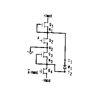
FIG. 1 is a schematic diagram of a quantum well
modulator driver circuit constructed in accordance with the
present invention;
FIG. 2 is a schematic diagram of a differential
quantum well modulator driver circuit;
FIG. 3 is a schematic diagram of the circuit of
FIG. 2 modified to include diode configurations for deriving
the complementary input signals; and
FIG. 4 is a schematic diagram of another differential
quantum well modulator driver circuit.
DETAILED DESCRIPTION OF THE PREFERRED EMBODIMENT
Referring now to the drawings, and initially to
FIG. 1 thereof, a schematic diagram of an optical quantum well
modulator driver circuit is schematically depicted. The
circuit is comprised of four transistors Q1, Qz, Q3, Q4. here
field effect transistors (FETs), and a quantum well modulator
Ml having terminals T1 and T2. As shown, terminal T1 is
connected to the drain of transistor QZ and terminal TZ is
connected to the drain of transistor Q4. The source of QZ and
the drain of Q3 are connected to each other and form a
junction at node N2. Transistor Q1 is operated at a first
reference voltage of +Vmoa and transistor Q4 is operated at a
second reference voltage of -Vmod. Node NZ is maintained at a
third reference voltage which, in the preferred embodiment, is
held at ground. Also as shown, the gate of transistor QZ
receives a first input signal (A) and the gate of transistor
Q4 receives a second input signal having a voltage value of
the logical complement of A, i . a . A less Vmod, i . a . (A-Vmod)
Transistor pairs Ql, Q2, Q3. Q4 form first and second switching
CA 02146800 1998-08-04
- 6 -
means, respectively, for applying voltages to M1 in a manner
more fully described below.
The circuit of FIG. 1 operates in the following
manner. When first input signal A is high relative to ground,
transistor Qz will turn on, thereby pulling node N1 to ground
and causing the voltage at terminal T1 to assume the value of
the third reference voltage which, as explained above, is
ground in the preferred embodiment. Simultaneously with first
input signal A going high, second input signal A-Vmod is low
relative to -Vmod. Thus, Q4 remains in its off state. Since
Q3 is always on, when Q4 is off node N3 is also at ground,
thereby causing the voltage at terminal TZ to be at ground
potential. Thus, it should be apparent that when first input
signal A is high, the voltage drop across modulator M1 is
0 volts.
Transistor Q1, like transistor Q3, is also always on,
i.e. operating in a low-resistance state. Thus, when first
input signal A is low, transistor Qz turns off, thereby
causing the voltage at node N1 and terminal T1 to be
approximately Vmoa. When first input signal A is low, second
input signal A-Vmoa is high, thereby turning on transistor Q4
which changes the voltage at node N3 and terminal TZ to -Vmoa.
Therefore, if A is low., the voltage drop across modulator M1
is approximately 2Vmod. It will accordingly be recognized that
this circuit effectively limits the voltage across any of the
transistors to a maximum of Vmoa while allowing a maximum
voltage drop of 2Vmoa across modulator Ml. As explained above,
this result is particularly beneficial because it permits the
use of modulators whose optical performance is superior to
similar devices restricted to operation at a lower voltage.
Attention is now directed to FIG. 2 which depicts a
differential modulator drive circuit in accordance with the
present invention. This is a symmetrical circuit whereby the
left-hand portion of the circuit is responsive to input
signals A and A-Vmod while the right-hand portion is responsive
to input signals A and A-Vmod. Specifically, the gates of
transistors QZ and QB receive input signals A and A-Vmoa,
CA 02146800 1998-08-04
- 6a -
respectively, and the gates of transistors Q6 and Q4 receive
input signals A and A-Vmoa. respectively. Transistors Q1, Q2,
Q3, Q4, along with modulator Ml, are configured in an identical
manner to that of FIG. 1. However, this circuit differs from
the FIG. 1 arrangement in that it further includes transistors
525. Q6. Q,. Q8 and a second modulator M2.
As shown in FIG. 2, the source of transistor QS and
the drain of transistor Q6 are joined at node NS which is
connected to terminal T3 of modulator M2. Likewise,
transistors Q., and Q8 are similarly joined at node N6, which is
connected to terminal T4 of modulator M2. Transistors Q1 and
QS are operated at a first reference voltage of +Vmoa and
transistors Q4 and Qg are operated at a second reference
voltage of -Vmod
When first input signal A is high, transistor Q2 will
turn on, thereby pulling node N1 to ground and causing the
reference voltage (zero volts) to appear at terminal T1 of
modulator M1. While input signal A is high, second input
signal A-Vmod is low which causes transistor Q4 to remain off.
This causes node N3 to be pulled to ground and causes zero
volts to appear at terminal Tz. Thus, the voltage drop across
modulator M1 will be zero volts when input signal A is high.
Also when input signal A is high, third input
signal A -- which is the complement of A -- will be low,
~~~~~o~
thus causing transistor Q6 to remain off. This creates a
voltage of +Vmoa at node NS which will also appear at
terminal T3 of modulator M2. In addition, fourth input
signal A-Vmoa will be high and turn on transistor Q8 which
creates a voltage at terminal T4 of approximately -Vmoa.
Thus, it will be seen that when input signal A is high the
voltage drop across modulator Mz has a value of 2Vmoa and the
voltage drop across modulator Ml is zero. Conversely, when
first input signal A is low, the opposite result occurs --
i , a . the voltage across modulator Ml is 2Vmoa and the voltage
across modulator Mz is zero.
The circuit of FIG. 2 allows the bright and dark
contrasts of the modulators M1 and MZ to be easily detected
because the optical signals generated by the respective
modulators M1, Mz can be compared one to the other. Thus,
the differential modulator driver circuit of FIG. 2
advantageously enables ready comparison of the high signal
to the low signal so as to determine whether what is
believed to be the high signal is, indeed, at a high state.
Turning now to FIG. 3, the differential modulator
driver circuit of FIG. 2 is shown modified to further
incorporate two diode chains or configurations. The first
diode configuration is comprised of diodes Dl, D2, D3, D4 and
transistor Q9, and the second diode configuration is
comprised of diodes D5, D6, D" D8 and transistor Qlo. The
first diode configuration is configured for passing to the
left-hand portion of the circuit the first and third input
signal s , A and A-Vmoa . Thus , diodes Dl , DZ , D3 and D4 are
chosen to create a voltage drop sufficient to equal the
value of Vmoa and thereby provide the third input signal A-
Vmoa~ Likewise, at the right-hand portion of the circuit,
diodes D5, D6, D., and DB are also selected to create a
voltage drop of Vmoa so that the second input signal that is
applied to the gate of transistor Q4 will be A-Vmod. Thus,
although the FIG. 3 arrangement operatively requires four
2~4~~'~
_8_
different input signals, only two of those signals, namely
A and A, need to be expressly provided with the first and
second diode configurations generating the remaining two
input signals, A-Vmoa and A-mod
Referring now to FIG. 4, a most preferred
differential modulator driver circuit is there shown. In
this final circuit arrangement, transistor Q1z has a fixed
gate voltage -V~ having a value slightly greater than the
value of -Vmoa. Thus, by way of example, if Vmoa is 4 volts
so that -Vmoa iS -4 volts, -V~ may be -3 volts. It is noted
that -V~ may be externally applied or may be derived from
one of the reference voltages . Each modulator Ml, Mz has one
of its terminals tied to +Vmoa and -Vmod, respectively. When
first input signal A is low so that second input signal A-
Vmoa is also low, transistors Q2, Q8 and Q12 are off and
transistor Qll is on. This places a voltage of Vmoa at node
NS and causes the voltage drop across modulator Ml to be zero
volts and the voltage drop across modulator MZ to be 2Vmoa.
When the opposite state or value of the first input signal
is applied -- i . e. A is high and A-Vmoa is more positive than
-Vmoa -- transistors Qz, Q$ and Qlz are on and transistor Q11
is off. In that case, the voltage at node NS is -Vmoa which
causes the voltage drop across modulator M1 to be 2Vmoa and
the voltage drop across modulator M2 to be zero.
Accordingly, as in the circuit of FIG. 2, the FIG. 4
arrangement simultaneously generates a bright and a dark
signal from the two modulators, thus readily permitting
comparison of one to the other so as to determine which
signal corresponds to a high and which signal corresponds to
a low.
It should be pointed out that although the circuit
of FIG. 4 achieves the same result as the circuit of FIG. 2
in that both simultaneously generate two opposite-state
optical signals, the circuit of FIG. 4 provides additional
benefits. Specifically, unlike the FIG. 2 arrangement which
- g _
requires the external provision of two separate input
signals -- namely, A and A -- the circuit of FIG. 4 requires
only one input signal (A). The second input signal for the
FIG. 4 circuit, namely A-Vmoa, is derived by utilizing a
diode configuration similar to that depicted in FIG. 3. In
addition, only 6 transistors are required for the circuit of
FIG. 4, whereas 8 transistors are required for the FIG. 2
arrangement. Since the circuit of FIG. 4 utilizes fewer
transistors, it correspondingly -- and advantageously --
occupies less area on a chip containing the circuit.
Finally, it is clear that the principles employed in the
circuit of FIG. 4 are readily extensible to additional
stages which may yield even higher voltages.
In a most preferred embodiment, the transistors
are implemented using GaAs FETs designed for operation at a
maximum voltage of 4 volts, i.e. Vmoa=4 volts. Thus, and as
should by now be apparent to one having ordinary skill in
the art, the inventive driver circuits described herein
create across the modulators a maximum voltage drop which is
greater than the maximum voltage applied to the transistors.
This higher voltage creates an extended and enhanced
contrast between the opposite-state dark and light optical
signals generated by the modulators.
Although I have herein shown and described the
currently preferred embodiments of the invention, various
changes and modifications of those expressly described
embodiments will be readily apparent to those of ordinary
skill in the art who read the foregoing description. In
addition, it is further contemplated that silicon
transistors may be used as a substitute for Gags transistors
and that the transistors used may be capable of safely
operating at voltages above or other than 4 volts. Thus,
the preferred embodiments and examples described herein are
for illustrative purposes only and are not to be construed
as limiting the scope of the present invention, which is
- 10 -
properly delineated only in the appended claims.