Note: Descriptions are shown in the official language in which they were submitted.
21~69 24 ~
DESCRIPTION
OPTICAL DEVICE FOR CODE READER
Technical Field:
The invention of the present application relates
to an optical device for a code reader for reading a code
such as bar code or the like imprinted on the package or the
like of an article.
Background Art:
Fig. 6 shows a prior art of an optical device for
a bar code reader as one of the examples of an optical
device for a code reader (see, e.g., the Japanese Patent
Laid Open Publication No. 276877/1992). In this prior art,
laser light emitted from a laser diode 31 is first converged
by a collimator lens 32, thereafter reshaped by a slit 33
and thus made a laser beam 34 having an elliptic or flat
oval cross section.
The laser beam 34 is reflected by both a rotating
polygon mirror 35 and a group of reflecting mirrors 36,
becomes incident on a bar code 37 to be read and scans over
that bar code 37. The laser light reflected by the bar code
37 is converged by a condenser lens 38 and becomes incident
on a photodiode 39. The bar code 37 is read by way of a
conversion of the received light signal to an electric
signal and a subsequent output by the photodiode 39.
In the prior art explained above so far, as is
2 1 ~ 4
-
apparent from Fig. 6, discrete parts such as the laser diode
31 as a light emitting element, the photodiode 39 as a light
receiving element, and the like are assembled and fixed by
adhesion or the like.
As, however, a conventional optical device for a
bar code reader, with assembled discrete parts, required
spaces for combining parts with inherent size, there was a
limitation in reducing its size and weight. In addition,
such a device also required a high precision adjustment in
the order of about 10 ~m of the relative position between
the discrete parts, and this adjustment was not easy so that
the production cost got high. Furthermore, after the
assembly had been completed, there was a possibility of
alteration with age of the relative position between the
discrete parts, and this gave a limitation to the
reliability.
Disclosure of Invention:
The invention of the present application is
achieved in view of the circumstances explained above and
has objects of reducing the size, the weight and the
production cost and improving the reliability of an optical
device for a code reader.
In the optical device for a code reader according
to the invention of the present application, a light
emitting element, a prism and a light receiving element are
all fixed to a semiconductor substrate, so that an assembly
at the semiconductor chip level of these elements is
--2--
21~924
possible. As a result of this, reduction of both the size
and the weight is now possible; the production cost is kept
low since, by using the high-precision packaging technology
for semiconductor device, an adjustment of the relative
position between the each element is easily feasible; and,
moreover, the reliability is made higher since the
alteration with age of the relative position and the like
are excluded as sealing those elements in one package
altogether is now possible.
The numerical aperture of the light converging
element is larger than that of a reflecting film which
reflects the light for irradiating the code, so that, even
if the irradiated light on the code is scattered, this
scattered light can effectively be converged. As a result
of this, even if the surface of the portion on which the
code is imprinted is not flat and smooth, the code can be
read with high probability and a high reliability is
obtained.
If an off-axis element is provided, freedom of
positioning the light receiving element gets larger.
Moreover, there can be prevented the light, once reflected
by the code and converged by the light receiving element,
from returning to the light emitting element after incidence
on the reflecting film. As a result of this, even a
semiconductor laser or the like can as the light emitting
element let the light stably irradiate the code so that the
code can be read with high probability and a high
21~6924
reliability is obtained.
If a light absorbing film is provided on the
prism, there can be prevented the light, once emitted from
the light emitting element with a wider angle than the
numerical aperture of the reflecting film, from incidence as
stray light on the light receiving element, so that the code
can be read with higher S/N. As a result of this, the code
can be read with high probability and a high reliability is
obtained.
Brief Description of Drawings:
Fig. 1 shows a side view of the first embodiment
according to the invention of the present application.
Fig. 2 shows a side view of the second embodiment
according to the invention of the present application.
Fig. 3 shows a side view of the third embodiment
according to the invention of the present application.
Fig. 4 shows a side view of the fourth embodiment
according to the invention of the present application.
Fig. 5 shows a side view of the fifth embodiment
according to the invention of the present application.
Fig. 6 shows a perspective view of a prior art
according to the invention of the present application.
Best Mode for Carrying Out the Invention:
The first to fifth embodiments according to the
invention of the present application applied to an optical
device for a bar code reader will be described hereinafter
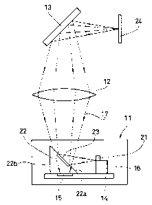
referring to Figs. 1 to 5. Fig. 1 shows the first
--4--
~ 2146924
embodiment. The first embodiment comprises a complex
optical element 11 for a bar code reader, a light converging
lens 12 and a swingable mirror 13.
The complex optical element 11 for a bar code
reader includes a semiconductor chip 14 such as a silicon
chip or the like; a photodiode 15 is formed in a region of a
surface of this semiconductor chip 14. On another region on
the semiconductor chip 14 than the region where the
photodiode 15 is formed, there is fixed a submount 16 for
adjustment of height; a laser diode 21 emitting a laser
light 17 is fixed on the submount 16.
On the photodiode 15, there is fixed a prism 22
having a right-angled triangle shaped cross section and an
inclined surface 22a orientated toward the laser diode 21.
On one region of the inclined surface 22a, there is provided
a reflecting film 23 which works as either a mirror or a
half mirror for the laser light 17; the laser light 17
incident on the rest of the inclined surface 22a is all
transmitted.
The reflecting film 23 is shaped such that it
constitutes an aperture when looked from the laser diode 21
toward the prism 22; if the aperture is, e.g., circular, the
reflecting film 23 looks circular when the prism 22 is
looked from the laser diode 21. On the other hand, the lens
12 has a larger numerical aperture than the aperture formed
by the reflecting film 23.
In the first embodiment having the constitution as
- ` 2146924
described above so far, the laser light 17 emitted from the
laser diode 21 is reflected upward by the reflecting film
23, converged by the lens 12, reflected further by the
mirror 13, and focused on the bar code 24 to be read. At
this time, the mirror 13 is swung, and the laser light 17
scans over the bar code 24.
The laser light 17 reflected by the bar code 24 is
reflected by the mirror 13, converged by the lens 12, and
becomes incident on the inclined surface 22a. The laser
light 17 incident on other regions than the region of the
reflecting film 23 in the inclined surface 22a transmits
through this inclined surface 22a and becomes incident on
the photodiode 15.
The laser light 17 incident on the region of the
reflecting film 23 in the inclined surface 22a is, if the
reflecting film 23 is a mirror, reflected toward the laser
diode 21; if the reflecting film 23 is a half mirror, a part
of the laser light 17 becomes incident on the photodiode 15
while the rest is reflected toward the laser diode 21.
In this case, the amount of the laser light 17
incident on the photodiode 15 varies depending on the
reflectance of the bar code 24 so that the bar code 24 can
be recognized by way of that signal. Question as to whether
a mirror or a half mirror should be adopted as the
reflecting film 23, or, if a half mirror is adopted, how
large its reflectance should be, is to be answered by
considering the magnitude of scattering of the laser light
--6--
2146924
17 by the bar code 24; the reflectance of the reflecting
film 23 should be made larger with increasing magnitude of
the scattering.
In the first embodiment, only the photodiode 15 is
formed on the semiconductor chip 14. In addition to the
photodiode 15, however, a voltage converter of signal
current, an AD converter for conversion of analog signals to
digital signals, and the like can also be formed there.
Fig. 2 shows the second embodiment. While the
first embodiment as explained above is of an in-line type
where the optical axis of the laser light 17 reflected by
the bar code 24 and incident on the lens 12 coincides with
that of the laser light 17 converged by that lens 12, the
second embodiment is of an off-axis type where those axes do
not coincide with each other and the photodiode 15 is not
located under the prism 22.
For this, in the second embodiment, there is
placed a prism 25 having in its central portion a through
hole 25a, on the side, relative to the lens 12, of a complex
optical element 11 for a bar code reader. Consequently, the
laser light 17 emitted from the laser diode 21 and reflected
by the reflecting film 23 goes straight ahead through the
through hole 25a and becomes incident on the lens 12; the
laser light 17 scattered by the bar code 24 and converged by
the lens 12 is deflected by the prism 25 and becomes
incident on the photodiode 15.
Fig. 3 shows the third embodiment. This third
2146924
embodiment is constituted in essentially the same way as the
second embodiment shown in Fig. 2 except that a hologram 26
having in its central portion a through hole 26a is used
instead of the prism 25; the third embodiment executes the
same function as the second embodiment does.
Fig. 4 shows the fourth embodiment. This fourth
embodiment is constituted in essentially the same way as the
third embodiment shown in Fig. 3 except that a hologram 27
executes the same function as that of the lens 12 and the
hologram 26. That is, the central portion 27a of the
hologram 27 executes the convergence function only while the
surrounding portion 27b executes both the convergence
function and the refraction function.
Fig. 5 shows the fifth embodiment. The fifth
embodiment is constituted in essentially the same way as the
second to fourth embodiments except that the photo diode 15
is formed in another semiconductor chip 28 than the
semiconductor chip 14, and that the semiconductor chip 28 is
fixed in another region than the region under the prism 22
within the semiconductor chip 14, while in the above-
mentioned second to fourth embodiments, the photo diode 15
is within the semiconductor chip 14 formed in another region
than the region under the prism 22.
If, in the above-mentioned second to fourth
embodiments, a light-absorbing film (not shown in the
figures) is provided on the vertical surface 22b of the
prism 22 on the side of the photo diode 15, the laser light
2146924
17 emitted from the laser diode 21 with a wider angle than
the numerical aperture of the reflecting film 23 can be
prevented from incidence as stray light on the photo diode
15 as it is.
In all the above-mentioned first to fifth
embodiments, the invention of the present application is
applied to an optical device for a bar code reader. As a
matter of course, however, the invention of the present
application can also be applied to optical devices for
reading a code other than bar code, such as Carla code or
the like.
Industrial Applicability:
The optical device for a code reader according to
the invention of the present application can be used as an
optical apparatus for reading various codes such as bar
code, Carla code and the like used in POS systems, physical
distribution/management systems, production control systems,
and so forth.