Language selection

Search

Patent 2146941 Summary

Third-party information liability

Some of the information on this Web page has been provided by external sources. The Government of Canada is not responsible for the accuracy, reliability or currency of the information supplied by external sources. Users wishing to rely upon this information should consult directly with the source of the information. Content provided by external sources is not subject to official languages, privacy and accessibility requirements.

Claims and Abstract availability

Any discrepancies in the text and image of the Claims and Abstract are due to differing posting times. Text of the Claims and Abstract are posted:

  • At the time the application is open to public inspection;
  • At the time of issue of the patent (grant).
(12) Patent: (11) CA 2146941
(54) English Title: OVERVOLTAGE PROTECTION
(54) French Title: PROTECTION CONTRE LES SURTENSIONS
Status: Expired and beyond the Period of Reversal
Bibliographic Data
(51) International Patent Classification (IPC):
  • H02H 07/20 (2006.01)
  • H02H 03/20 (2006.01)
  • H02H 09/04 (2006.01)
(72) Inventors :
  • SUUR-ASKOLA, SEPPO (Finland)
(73) Owners :
  • KONE OY
(71) Applicants :
  • KONE OY (Finland)
(74) Agent: G. RONALD BELL & ASSOCIATES
(74) Associate agent:
(45) Issued: 2001-01-02
(22) Filed Date: 1995-04-12
(41) Open to Public Inspection: 1995-10-15
Examination requested: 1996-04-29
Availability of licence: N/A
Dedicated to the Public: N/A
(25) Language of filing: English

Patent Cooperation Treaty (PCT): No

(30) Application Priority Data:
Application No. Country/Territory Date
FI 941720 (Finland) 1994-04-14

Abstracts

English Abstract


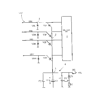
A method and apparatus for protecting an I/O electronic circuit against
overvoltages includes a first current path comprising a first diode (V1N),
through which
current path a current (ip) flows when the overvoltage is negative. A second
current path
includes a second diode (V1P) and a thyristor (T1), the thyristor (T1) being
fired by means
of a time-delay circuit charged by a positive voltage. Current flowing through
the current
paths is used to trigger a protection device, such as a circuit breaker, to
cut off the
overvoltage power supply.


Claims

Note: Claims are shown in the official language in which they were submitted.


7
THE EMBODIMENTS OF THE INVENTION IN WHICH AN EXCLUSIVE PROPERTY
OR PRIVILEGE IS CLAIMED ARE DEFINED AS FOLLOWS:
1. A method for protecting an I/O circuit of an electronic circuit
against overvoltages, comprising the steps of:
(a) connecting the I/O circuit of the electronic circuit to a current path
comprising a first diode through which current flows when the voltage on the
I/O
circuit is a negative overvoltage;
(b) providing the I/O circuit of the electronic circuit with a second
current path comprising a second diode connected in series to a time-delay
circuit at
a first node; the time-delay circuit including a thyristor connected between
the first
node and ground and having a gate, a Zener diode connected in series with a
first
resistance between the first node and ground, and a second resistance
connected
between the gate and a second node linking the Zener diode and the first
resistance,
whereby the thyristor is fired by a time-delay in the time-delay circuit when
the
voltage on the I/O circuit is a positive overvoltage, the current flowing
through the
current paths providing the overvoltage protection.
2. The method according to claim 1, further including the step of:
(c) providing a first capacitor connected to the time-delay circuit in
parallel with the thyristor, and a second capacitor for removing transient
interference
voltage peaks.

8
3. The method according to claim 1 or 2, further including the step
of providing the first diode, the second diode, and the thyristor with current
ratings
exceeding the fusing value of a mains fuse included in the secondary circuit
of a
decoupling transformer.
4. The method according to claim 3, further including the step of
connecting the time-delay circuit to a plurality of I/O circuits.
5. The method of claim 2, wherein said step (c) includes connecting
said second capacitor in parallel with said first capacitor.
6. An apparatus for protecting an input/output circuit of an electronic
circuit against overvoltages, comprising:
a conductor for the input/output circuit of the electronic circuit;
a first reverse-biased diode having an anode connected to ground and
a cathode connected to said conductor;
a second forward-biased diode connected between the conductor and
a first node; and
a time-delay circuit connected between the first node and ground, said
time-delay circuit including a first capacitor and a thyristor connected in
parallel
between the first node and ground, a gate of said thyristor being connected
through
a Zener diode to the node and to a cathode of said second diode.

9
7. The apparatus according to claim 6, further including a plurality of
conductors, each for a respective I/O circuit and connected through respective
first
reverse-biased diodes to ground and through respective second forward-biased
diodes to the first node, wherein the first and second diodes are connected as
a
bridge circuit.
8. The apparatus of claim 7, wherein said time-delay circuit further
includes:
a second resistance connected between said Zener diode and the gate
of said thyristor, said second resistance connecting to said Zener diode at a
second
node;
a first resistance connected between the second node and ground;
a third resistance connected between said first node and a positive
voltage source; and
a second capacitor connected in parallel with said first capacitor between
said first node and ground, said second capacitor having a smaller capacitance
than
said first capacitor and absorbing transient voltage peaks at said first node.
9. The apparatus of claim 6, wherein said time-delay circuit further
includes a resistance connected between said Zener diode and the gate of said
thyristor.

10
10. The apparatus of claim 9, wherein said resistance connects to said
Zener diode at a second node, and further including another resistance
connected
between the second node and ground.
11. The apparatus of claim 6, wherein said time-delay circuit further
includes a resistance connected between said first node and a positive voltage
source.

Description

Note: Descriptions are shown in the official language in which they were submitted.


2~4~941
1
OVERVOLTAGE PROTECTION
The present invention relates to a method for protecting input/output
circuits against overvoltages.
Overvoltages occur every now and then and they cause damage in
sensitive I/O electronics. I/O voltages are generally of the order of 0 - 32
V. For
example, if a mains voltage (e.g. 240V, 60 Hz) happens to be applied to an I/O
pin,
ordinary I/O electronic circuits will be damaged beyond repair. This results
in
maintenance problems and increased costs. There are various components, such
as varistors and overvoltage Zener diodes, for protection against lightning
and
instantaneous overvoltages. However, if a mains voltage of, for example, 240V,
is
supplied directly to an electronic circuit, such conventional protection
components will
not withstand it. If an installer makes a mistake, high voltage may be
connected
directly from the mains to low-voltage circuits, and this will result in
further damage
to equipment and safety risks. The conventional circuit protection components
cannot endure a voltage of 240V and they have a very limited power capacity.
An object of the present invention is to provide a method and apparatus
for protecting I/O circuits from high voltages.
According to an aspect of the present invention there is provided a
method for protecting an I/O circuit of an electronic circuit against
overvoltages,
comprising the steps of:

2146941
2
(a) connecting the I/O circuit of the electronic circuit to a current path
comprising a
first diode through which current flows when the voltage on the I/O circuit is
a
negative overvoltage; (b) providing the I/O circuit of the electronic circuit
with a
second current path comprising a second diode connected in series to a time-
delay
circuit at a first node; the time-delay circuit including a thyristor
connected between
the first node and ground and having a gate, a Zener diode connected in series
with
a first resistance between the first node and ground, and a second resistance
connected between the gate and a second node linking the Zener diode and the
first
resistance, whereby the thyristor is fired by a time-delay in the time-delay
circuit
when the voltage on the I/O circuit is a positive overvoltage, the current
flowing
through the current paths providing the overvoltage protection.
According to a further aspect of the present invention there is provided
an apparatus for protecting an input/output circuit of an electronic circuit
against
overvoltages, comprising: a conductor for the input/output circuit of the
electronic
circuit; a first reverse-biased diode having an anode connected to ground and
a
cathode connected to said conductor; a second forward-biased diode connected
between the conductor and a first node; and a time-delay circuit connected
between
the first node and ground, said time-delay circuit including a first capacitor
and a
thyristor connected in parallel between the first node and ground, a gate of
said
thyristor being connected through a Zener diode to the node and to a cathode
of
said second diode.

214fi941
3
The method and apparatus of the invention prevent the application of an
overvoltage to sensitive I/O electronics in the event of a malfunction. In the
protection system according to the present invention, the voltage at an I/O
pin will
never exceed the allowed values. The invention provides the following
advantages:
- it does not cause any change in the operating points of the I/O;
electronics or in any other delays or impedances of the I/O
electronics;
- simple I/O lines and connections can be used;
- the invention is inexpensive, particularly when there are a large
number of I/O lines;
- the invention allows high data transmission speeds;
- the invention filters radio-frequency interference;
- the invention requires no additional filters; and
- the invention can be installed as a retrofitable option in old
systems, enabling existing circuits to be modernised by the
addition of the circuit protection arrangement in accordance with
the present invention.
In the following, the invention is described in detail by the aid of an
example by referring to the attached drawings representing the operation of
the
protection circuit.
Figure 1 shows a schematic illustration of a protection circuit in
accordance with an embodiment of the present invention.

21 469 41
4
Figure 2 presents a diode bridge used to replace diodes V1 N, V2N, V1 P
and V2P illustrated in Figure 1.
The operation of the protection circuit is illustrated in Figure 1.
Comprised in the overvoltage protection circuitry is pin I/01, which belongs
to the
electronic circuit and is the starting point of a current path 1. Connected to
pin I/01
is a diode V1 N, whose anode is connected to ground. The current path 1
continues
further to an electronics unit 5, for which overvoltage protection is to be
provided.
The anode of a second diode V1 P is also connected to this current path 1. A
current
ip flows along current path 1 via diode V1 P and further along current path 2
via pin
3 to circuit 4, which is common to all the I/O circuits, and in this circuit
to capacitor
C1, which is connected in parallel with capacitor C2, both of which are
connected to
ground. Connected in parallel with capacitor C1 is also a thyristor T1, whose
gate
is connected to a resistor R2. The other end of this resistor R2 is connected
via
resistor R1 to ground and via Zener diode Z1 and pin 3 to conductor 2. A power
source +Vs is connected via resistor R3 to pin 3. A time-delay circuit is thus
formed
by the first capacitor C1 and the thyristor connected in parallel with it, the
thyristor
firing circuit being connected via Zener diode Z1 to pin 3.
Figure 2 presents a diode bridge which can be used to replace diodes
V1 N, V2N, V1 P and V2P in Figure 1. The diode bridge is a commonly known
circuit.
The mains voltage VAC is a voltage obtained from the public network
and is commonly used as an energy source in instrument panels. In the event of
a
malfunction, the mains voltage VAC may be supplied to an I/O line.

_. 214694
If the mains voltage VAC is negative at the instant the malfunction
occurs, then it follows that the current ip will flow along current path 1
from pin I/01
via diode V1 N to ground. The high current passing through this path blows the
fuse
or circuit-breaker of the VAC source, and thereby terminates the supply of
VAC. This
5 fuse or circuit-breaker is the common electricity supply fuse (or breaker)
of the
instrument panel and is typically placed in the secondary circuit of a
decoupling
transformer.
If the mains voltage VAC is positive at the moment of malfunction, then
it follows that the current ip will flow along current path 1 via the first
diode V1 P and
further along current path 2 to pin 3 and to capacitor C1 in circuit 4. In a
normal
situation, C1 is charged to voltage +Vs via resistor R3. +Vs is a voltage
source (for
example 24V) and its function is to keep the triggering limit of the
protection circuit
above the normal instrument panel supply voltage. The current ip charges
capacitor
C1 until the voltage VC1 exceeds the triggering level of the Zener diode Z1.
VC1 is
a voltage to which the capacitor C1 may be charged before the thyristor is
fired and
discharges capacitors C1 and C2. When the triggering level is exceeded, the
Zener
diode Z1 begins to conduct, and a current is passed to the gate of the
thyristor via
resistor R2. This current switches the thyristor T1 into conduction, so that
the current
ip will now flow through the thyristor T1 to ground until the fuse or circuit-
breaker of
the VAC source is blown. Resistor R1, which is connected to ground, prevents
spurious firing of the thyristor.

21~6g~'
6
Resistor R1, connected between the gate and cathode of the thyristor
T1, is designed to reduce the impedance of the gate circuit and to pass
spurious
energies past the gate to the cathode, thus preventing the gate voltage from
rising
to the firing level under normal operating conditions (i.e. when VAC is not
being
supplied to one of the I/O input pins I/01...1/ON). Capacitor C2, connected in
parallel
with capacitor C1, receives transient interference peaks. The diodes V1 N-VNN
and
V1 P-VNP and the thyristor T1 must have current ratings exceeding the fusing
value
of the fuse or circuit breaker. The current flowing through current paths 1
and 2 is
used to trigger the protection device. An unlimited number of I/O lines can be
connected. to the protection circuit 4 by this means.
It will be obvious to a person skilled in the art that different embodiments
of the invention are not restricted to the examples described above, but that
they may
instead be varied within the scope of the claims presented below. For
instance, the
thyristor can be replaced with a triac, transistor, GTO thyristor or IGBT
transistors.

Representative Drawing
A single figure which represents the drawing illustrating the invention.
Administrative Status

2024-08-01:As part of the Next Generation Patents (NGP) transition, the Canadian Patents Database (CPD) now contains a more detailed Event History, which replicates the Event Log of our new back-office solution.

Please note that "Inactive:" events refers to events no longer in use in our new back-office solution.

For a clearer understanding of the status of the application/patent presented on this page, the site Disclaimer , as well as the definitions for Patent , Event History , Maintenance Fee  and Payment History  should be consulted.

Event History

Description Date
Time Limit for Reversal Expired 2006-04-12
Inactive: IPC from MCD 2006-03-11
Letter Sent 2005-04-12
Grant by Issuance 2001-01-02
Inactive: Cover page published 2001-01-01
Pre-grant 2000-09-19
Inactive: Final fee received 2000-09-19
Letter Sent 2000-07-05
Amendment After Allowance Requirements Determined Compliant 2000-07-05
Amendment After Allowance (AAA) Received 2000-06-16
Letter Sent 2000-03-27
Notice of Allowance is Issued 2000-03-27
Inactive: Status info is complete as of Log entry date 2000-03-21
Inactive: Application prosecuted on TS as of Log entry date 2000-03-21
Inactive: Approved for allowance (AFA) 2000-03-06
Deemed Abandoned - Failure to Respond to Maintenance Fee Notice 1997-04-14
Inactive: Adhoc Request Documented 1997-04-14
All Requirements for Examination Determined Compliant 1996-04-29
Request for Examination Requirements Determined Compliant 1996-04-29
Application Published (Open to Public Inspection) 1995-10-15

Abandonment History

Abandonment Date Reason Reinstatement Date
1997-04-14

Maintenance Fee

The last payment was received on 2000-04-03

Note : If the full payment has not been received on or before the date indicated, a further fee may be required which may be one of the following

  • the reinstatement fee;
  • the late payment fee; or
  • additional fee to reverse deemed expiry.

Patent fees are adjusted on the 1st of January every year. The amounts above are the current amounts if received by December 31 of the current year.
Please refer to the CIPO Patent Fees web page to see all current fee amounts.

Fee History

Fee Type Anniversary Year Due Date Paid Date
MF (application, 3rd anniv.) - standard 03 1998-04-14 1998-04-03
MF (application, 4th anniv.) - standard 04 1999-04-12 1999-04-01
MF (application, 5th anniv.) - standard 05 2000-04-12 2000-04-03
Final fee - standard 2000-09-19
MF (patent, 6th anniv.) - standard 2001-04-12 2001-01-04
MF (patent, 7th anniv.) - standard 2002-04-12 2002-03-13
MF (patent, 8th anniv.) - standard 2003-04-14 2003-03-12
MF (patent, 9th anniv.) - standard 2004-04-12 2004-03-15
Owners on Record

Note: Records showing the ownership history in alphabetical order.

Current Owners on Record
KONE OY
Past Owners on Record
SEPPO SUUR-ASKOLA
Past Owners that do not appear in the "Owners on Record" listing will appear in other documentation within the application.
Documents

To view selected files, please enter reCAPTCHA code :


To view images, click a link in the Document Description column. To download the documents, select one or more checkboxes in the first column and then click the "Download Selected in PDF format (Zip Archive)" or the "Download Selected as Single PDF" button.

List of published and non-published patent-specific documents on the CPD .

If you have any difficulty accessing content, you can call the Client Service Centre at 1-866-997-1936 or send them an e-mail at CIPO Client Service Centre.


Document
Description 
Date
(yyyy-mm-dd) 
Number of pages   Size of Image (KB) 
Description 1995-10-14 5 175
Claims 1995-10-14 2 54
Drawings 1995-10-14 2 15
Abstract 1995-10-14 1 13
Description 2000-03-07 6 216
Claims 2000-03-07 4 106
Drawings 2000-03-07 2 18
Representative drawing 2000-12-13 1 5
Commissioner's Notice - Application Found Allowable 2000-03-26 1 164
Maintenance Fee Notice 2005-06-06 1 172
Correspondence 2000-09-18 1 31
Fees 1998-04-02 1 52
Fees 2001-01-03 1 45
Fees 1999-03-31 1 44
Correspondence 2000-07-04 1 6
Fees 2000-04-02 1 45
Fees 1997-04-03 1 54
Prosecution correspondence 1995-04-11 10 294
Prosecution correspondence 1999-11-17 2 62
Prosecution correspondence 1996-04-28 1 50
Examiner Requisition 1999-05-20 2 92
Prosecution correspondence 1996-06-19 2 45
Courtesy - Office Letter 1996-05-21 1 49
Prosecution correspondence 1996-06-19 2 59