Note: Descriptions are shown in the official language in which they were submitted.
CA 02147009 2001-12-12
METHOD AND DEVICE FOR THE PRODUCTION OF
OPTICAL LENSES OR THE LIKE
The invention relates to a method for the
production of optically functioning structures,
particularly of lenses and lens arrays and prisms in
which on the surface of a substrate in at least one
masking step with a subsequent etching step a basic
optically functioning base structure of steps or stages
is formed which is treated then in a melting step by
heating it until is smoothed by capillary surface forces
of the melted substrate.
A method of this general type is disclosed in
the magazine "Laser Focus World", 1991, pp. 93-99. In
this article an overview of the six different
conventional methods for producing microlenses and
microlens arrays is described. The closest method
includes the production of an approximately lens-shaped
structure on the surface of a substrate by means of
photolithographic masking and subsequent etching, which
is subjected to heat treatment, because of which a minor
mass transport results, which, with certain materials,
leads to qualitatively good lenses. The lithography is
performed with a plurality of masks that are respectively
aligned, so that the totality of the sequentially etched
and stepped structures approximately from the lens. The
heat treatment leads to
- 1 -
2147009
complete melting of the lens material and also of the
entire carrier substrate. During this melting the surface
tension produces a deformation of the entire surface and
of the lens mass as well as of the surrounding substrate;
although the stepped structure is reduced, the optical
parameters of the lens are changed drastically, leading to
optical errors and to severe dispersions and deviations of
the lens characteristics with respect to a respectively
given characteristic.
Moreover, it is known from the magazine
"Spektrum der Wissenschaft [Spectrum of Science]", 1992,
pp. 44-50, Veldkamp et al, Binary Optics, to etch a planar
diffractive lens into the planar face of a planar-convex
refractive lens, where the opposing color aberrations of
the refractive and the diffractive optics mutually
compensate each other and color fidelity is attained over
a broad spectral scope. The etched refractive lens,
however, produces a light scatter by means of its etched
end face-that reduces the image contrast. To avoid this
error over a wide wave range, a large number of masking
and etching steps are used, for example up to twelve,
wherein the etching is performed at a decreasing step
height. This means high production costs and causes a
considerable amount of rejections, i.e. unsatisfactory
product which is waste.
- 2 -
CA 02147009 2001-12-12
It is an object of the invention to overcome
deficiencies in the prior art, such as indicated above.
Another object is to provide a method and a device that
permit the industrial production of structured optical
arrangements, particularly lens arrays, with high
precision and narrow tolerances of the optical data, and
the resultant novel optical structures so produced.
These objects are attained by placing, during
the melting step, the substrate that carries the base
structure inside a vacuum chamber, and then moving the
base structure beneath and past a generally fan-shaped
high-voltage-accelerated electron beam, which projects
downwardly onto the substrate as the substrate moves
thereby, the plane at the electron beam defining the
front at a melting zone created by the electron beam on
the base structure, the beam being provided with such an
energy density that the melting zone has a depth that
corresponds to at least one step height of the stepped
base structure.
The electron beam is preferably produced with a
linear electron beam gun the anode voltage of which
amounts to several kilovolts, for example at least 2
kilovolts, preferably 2-5 kilovolts, so that the
radiation impacting upon the substrate ejects therefrom a
sufficient number of secondary electrons so that a
continual charging of the substrate is effected, and the
substrate is charged with respect to the electron source
- 3 -
CA 02147009 2001-12-12
to such a voltage that is lower than the energy of the
electrons of the electron beam. In this way the exact
measurement of the beam energy charge in the melting zone
of the substrate can be taken using the voltage or the
proportion of the electrons produced in the electron
source. In conjunction with the longitudinal rate of feed
of the substrate with respect to the melting zone, the
penetration depth of the melting zone into the substrate
can be controlled precisely. This allows selection of a
suitable melting zone width and depth for a respectively
given substrate adapted to its melting and surface
tension conditions, which leads to a well-defined
leveling of the steps that had resulted during the
preceding production step for the base structure.
The tension conditions between the anode
voltage and the voltage to which the substrate is charged
can be advantageously stabilized by arranging the
substrate on a carrier that has a specific conductivity
less, by at least one order of magnitude, than the
substrate.
It has proven to be advantageous to select the
melting zone approximately 1 to 5 step heights deep and
frequently even near a step height. The width of the
melting zone is generally designed to be several step
heights wide, and it is particularly at least 2 to 20
step heights wide.
- 4 -
214749
Another variability of the process is brought
about by the arrangement of a pre-heating muffle furnace
in the vacuum chamber in which the substrate is thermo-
statically heated before melting of the surface takes
place. It has proven to be advantageous to preheat the
substrate to within approximately 50 to 100 K below the
melting or softening temperature of the material of the
base structure. This facilitates, for example, the
melting of quartz, from which high-quality lenses and lens
arrays can be produced. Metals that can be used as, for
example, optical mirrors can also be melted by an electron
beam, and preheating is also recommended here.
Because the process of melting the surface and
therefore the removal of the stepped structure permits the
production of extraordinarily high-quality optics, it has
proven to be advantageous in some cases to use in a
corrective manner those deviations which occur from the
ideal shape, these being generated during etching and
progressive melting of zones respectively during
production of the masks. By doing this an additional
undercut is provided along the contours and a
directionally-oriented pre-distortion is made in the
masks, which leads to the removal of the production-
related errors during melting.
The masking and etching step or a varied
sequence of these can be performed with the standard
methods of photolithography, laser lighting of the mask
- 5 -
2147009
materials or electron beam lighting of the mask materials,
whereupon the etching step can be performed with a liquid
or gaseous etching medium, particularly also by plasma
etching or ion etching, depending on the type of substrate
and the required precision. In principle, a production of
the base structure can also be achieved by means of
mechanical processing.
The method is also particularly suited for
production of a confocal, planar lens arrangement the
steps of which are definitively inclined and rounded off
at the edges and bottoms in such a way that the
detrimental influences of the step end faces and possibly
those of the undercut are eliminated.
The high uniformity of the optical data of the
produced lenses of a lens array that are assured by the
present method permit its confocal construction for all
lenses by shaping the individual lenses aspherically and
correcting them during the melting step with respect to
the optical errors. By means of this operation optical
systems are produced that nearly have the aperture 1,
which is very difficult to achieve in conventionally
produced individual lenses.
As is known, the novel lenses or lens structures
can advantageously be applied as compensatory or
corrective lenses to a plane face of a refractive lens.
By means of the smoothing melting process in accordance
with the present invention, the properties reducing the
- 6 -
'~= 2I4~009
contrasts in the etched step structure are eliminated or
significantly reduced; so that a substantially lower
number of steps is sufficient to attain the same quality.
In general, a single step is adequate.
The corrective lens is arranged on a separate
plate in front of or behind the refractive lens. It is
also advantageous to provide the use of corrective lenses
in connection with high-quality individual lenses that are
measured after their production, for which a laser
scanner for example is used, image errors of which are
systematically evaluated. A corrective lens structure for
an individual case is calculated with the acquired
measurement data and the mask set is subsequently produced
that serves in the production of the corrective lenses.
Here, too, a low-dispersion corrective lens can also be
produced with few mask and etching steps because of the
subsequent melting of the steps during the surface
melting. The melting causes the formation of undulating
profiles_of the flat structures. The optical characteris-
tics of such structures can be well described mathemati-
cally, and the mask calculation can thus be performed with
high precision, because the structural changes caused by
the melting of the steps can be predetermined and taken
into account in the calculation. Besides the lenses, the
combination of the measured system having corrective
2I47Q~9
plates or corrective structures on planar surfaces can
also be applied to other optical systems, for example to
prisms or prism arrays.
Surface optical wave guide optics can also
advantageously be developed with the method in accordance
with the present invention. In this way confocal, sector-
shaped pattern structures or also lens-shaped recesses can
be created the focus of which lies in the surface optical
wave guide and is oriented to, for example, a narrow
filament-shaped or strip-shaped optical wave guide or
optical wave guide section.
Mirror surfaces of concave mirrors, concave
mirror arrays, optical grids, etc. can be produced by the
method. The structure can be made directly in high-
quality reflective metal surfaces, for example, of silver
or chromium, or they can be produced on a material that
can be later mirrored. The surface can advantageously be
vacuum-mirrored by feeding the substrate into a vacuum-
coating device of the vacuum chamber after completion of
the melting process.
The device for executing the method is advanta-
geously designed for a plurality of substrates that pass
in succession through a muffle furnace that performs the
preheating, and then are guided past the electron emitter.
The substrate feed is triggered in a controlled manner,
the same as the various electrodes and the electron source
are supplied in a controlled manner by a control device.
- 8 -
CA 02147009 2001-12-12
It has proven advantageous for the control to compare a
measurement signal of a beam sensor focused on the
melting zone with a preset emission value, and to perform
the control in such a way that the difference of the two
values is as close as possible to zero.
In a particularly preferred embodiment there is
provided in a method for the production from a base of an
optical element that has a series of steps of height on a
surface on said base, formed by at least one masking
step, a subsequent etching step, heating said surface to
effect melting of said surface, and smoothing of said
surface by capillary surface forces, the improvement
comprising: said melting being carried out by placing
said base inside a vacuum chamber, sweeping a fan-shaped
high-voltage accelerated electron beam over said base by
relative motion of said electron beam and said base so
that said electron beam impinges upon said base along a
line generally perpendicular to the motion, a plane of
the electron beam defining a front of a melting zone,
said electron beam being provided with an energy density
such as to create the melting zone having a depth into
said base that corresponds to at least one step height of
said base.
_ g _
CA 02147009 2001-12-12
Brief Description of Drawing
Advantageous embodiments are represented in
Figs. 1 through 5:
Fig. 1 schematically shows the course of the
method;
Fig. 2 shows a cross-section of a device for
executing the method;
Fig. 3 shows a cross-section through a
substrate;
Fig. 4 shows a view of a surface optical wave
guide having an optical structure; and
Fig. 5 shows an optical system that includes a
corrective plate.
Detailed Description of Embodiments
Fig. 1 shows a schematic view of the course of
the method. The substrate (1) is coated, irradiated and
opened in a first masking step (MS) and etched out in
step form in a subsequent etching step (AS). For planar
structures, one masking step and one etching step are
- 9a -
224'~Q09
sufficient; for multidimensional structures, these two
steps must be repeated several times with appropriate
masks. The substrate (1) having the base structure (10)
produced in this way is smoothed in the subsequent melting
step (SS). A preheating step (HS) can precede the melting
step (SS) in that the substrate (1) with the base
structure (10) is heated to a preheating temperature (VT)
that is close to the melting or softening temperature of
the base structure.
7.0 The melting step is effected by controlling the
energy density of the electron beam and the rate of feed
of the substrate (1) perpendicular to the vertical plane
defined by, or the extension of, the front of the melting
zone, i.e. the plane of the electron beam. As a control
value, the temperature of the melting zone is measured
with a beam sensor (45) and supplied to a control device
(ST) as an actual value. The melting step (SS) takes
place in a vacuum chamber (3). This controls the electron
gun and the feed drive of the substrate feeding device
(20). If the optical structure comprises mirror elements,
a mirror-coating step (VS), which is advantageously
effected by means of vacuum deposition in a vacuum
chamber, follows the melting step (SS).
On the basis of an optical measurement (OM) of
the optical data of the end product (EP), the respective
deviations from an ideal form are determined and
- 10
w 214'~~?09
correctively taken into account via a calculation step
(RS) in a mask production step (ME) for the production of
the masks ( 6 ) .
Fig. 2 shows the device for performing the
melting step. It comprises a vacuum chamber (3), which
encloses a feed device (20) such as a conveyor, which
feeds carriers (2) at a level of the substrate, on which
the substrates (1) are arranged. The carriers (2)
advantageously consist of highly-insulating aluminum
oxide. The carrier and substrates pass through a muffle
furnace (30), which is represented as being open, where
the preheating takes place. This oven is electrically
heated with thermostatic control. The carriers (2) with
the substrates (1) exit from the downstream end of the
oven (30) to the area of the electron beam (4).
cross-section perpendicular to
the plane of the electron beam is shown.
T he electrons are released in a
resistance wire that serves as an electron source (40) and
then accelerated in the direction of a slotted anode (41).
The anode is charged by a controlled high voltage of a few
kilovolts. Along the path to the anode (41), the
electrons pass focusing electrodes (42) on the side, which
are charged by a focusing voltage. The accelerated
- 11
~147Q09
electrons exit the anode slot as a linear electrode beam
(4) and charge the substrate below with the base structure
(10) thereupon.
A radiation detector (45) whose output signal is
supplied to a control device (ST) is arranged above the
melting zone which is being created in the area of impact
of the electron beam (4) on the substrate (1). This
control device controls the high voltage, the focus
voltage, the current of the electron source and the feed
rate of the feed device (20). It is useful that the
electrical heating of the muffle furnace (30) is
controlled via the control device (ST), wherein the signal
of a temperature sensor (31) is supplied to the control
device as the actual signal.
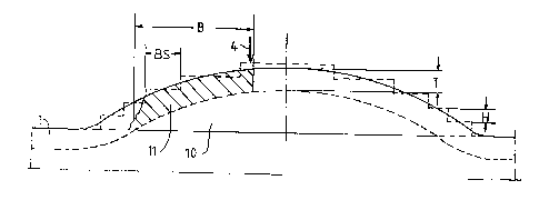
Fig. 3 shows, in a highly magnified manner, a
vertical section through a substrate that carries a lens.
The base structure (10) of the lens is shown in dot-dash
lines and has steps with a step height (H). A melting
zone (11)- of selected thickness is also represented, which
results from the charging by the electron beam (4) during
the continuous throughput of the substrate. This melting
zone (11) has a depth or thickness (T) that corresponds to
approximately 1.5 step heights (H) and has a width (B)
that overlaps, in this example, three mean step widths
(BS). The final form of the optical element is shown as
solid lines. This final form results during the melting
- 12 -
214'009
of the surface material as a result of the surface tension
of the melted mass. The surface tension equalizes and
eliminates the stepped structure and creates an approxi-
mately ideal optical surface. It can be seen that the
steps show a slight undercut that is, however, completely
eliirii.nated after melting.
Fig. 4 shows, in section and in perspective, a
planar optical device (PO) in a lithium niobate crystal,
in which a surface optical wave guide (WL) is embodied.
The optical arrangement is directed confocally toward the
focus (F). In this example, this focus lies on the edge
of the crystal, where a narrow fiber optical wave guide
strip (LL) is connected.
Fig. 5 shows a refractive, plano-convex lens (L)
on whose plane face a compensatory or corrective structure
(K*) has been produced in accordance with the method and
is embodied as undulating because of melting. The
compensatory structure (K*) is a planar lens that has a
color coefficient different from that of the refractive
lens (L), so that a wide-band color correction is attained
with low dispersion losses because of the undulating
structure. As an alternative, a corrective structure (K)
or a compensatory structure on a corrective plate (KP) is
produced, that is, placed in front of or behind one lens
(L) or, if need be, a plurality of lenses of a system.
- 13 -