Note: Descriptions are shown in the official language in which they were submitted.
21~7293
COMPOUND INDUCTORS FOR USE IN SWITCHING REGULATIONS
Technical Field
The present invention relates to switching regulators and
more specifically to a compound inductor for use in a switching
regulator having two or more asymmetrically coupled windings on
an equivalent number of magnetic cores.
Background Art
The market for modern switching power converters is
demanding higher power levels and power density. Meeting this
demand requires that components become smaller and dissipate less
power. Component size reductions generally require a increase in
switching frequency while improving efficiency. At the same time
electromagnetic interference (EMI) generated by the higher
frequency switching of voltages and currents must be at or below
prior art levels to meet federal and international requirements.
One approach to meeting these conflicting requirements is
the use of various so-called soft switching power converters. In
one type of power converter, the voltage is brought to zero on
the main switch or switches prior to turning on. When the switch
is turned off, the current transfers to the junction capacity of
the switch or switches or to additional capacity placed across
the switch or switches to assist in reducing EMI.
U.S. Patent 5,307,004 discloses soft switching circuits for
buck and boost regulators which utilize tapped main inductors.
In one embodiment, a small pilot inductor is disclosed in series
with the tap of the main inductor.
CA 02147293 1998-11-04
-2-
The use of discrete pilot and main inductors is known with the
pilot inductor consisting of a single winding on a core while
the main inductors consists of either a tapped winding on the
core or possibly a voltage bucking winding in addition to an
untapped winding to create the effect of a tap on the main
wlndlng .
The pilot inductance in our previously filed application
is small compared to the main inductor and the RMS current is
considerably less in the pilot inductor, although peak
currents are similar. Thus, the pilot inductor is
electrically smaller than the main inductor, but in practice
the dimensions of the pilot inductor are comparable to those
of the main inductor.
This discrepancy in relative sizes between the main
inductor and the pilot inductor is at least partially due to
the fact that while the main inductor current and flux are
largely DC with a smaller superimposed AC component, the
winding current and core flux in the pilot inductor pulse from
zero to maximum and back to zero very quickly. The pulse
duration is typically in the order of 5% to 10% of the
switching period, which generates strong harmonics of ten or
twenty times the switching frequency. Winding and core losses
increase dramatically with frequency above present switching
frequencies of 50 to 200 KHz, resulting in winding and core
losses in the order of three to ten time higher would be
expected from the RMS current and the peak-to-peak core flux
at the switching frequency.
Summary of the Invention
We have now found that if the core of the main inductor
is divided in two, the pilot inductor winding can be placed on
one of the two cores of the main inductor inside the main
inductor winding to create a
3 21~7293
compound inductor. This simultaneously provides the
e~uivalent of a voltage tap on the main inductor with the
pilot inductor in series with the voltage tap. Thus the
a~sembly for the main and pilot inductor~ ie
substantially the same size as known types of main
inductors. This results in switching regulators having
compound inductors that have reduced si~e, weight and
power losses over the use of conventional inductors.
Existing switching regulators often require two or
more stages of low pass filtering on the input and/or
output to meet ~MI requirements while minimizing the size
of the filter components. In the past this has required
the use of separate inductors for each ~ilter ~tage.
The present invention allows two or more low pass
filter inductors to be combined within the same compound
inductor construction resulting in size, weight and power
loss reductions over the use of two or more discrete
inductors.
The present invention provides a compound inductor
assembly comprising a first inductor having a first
winding on a first magnetic core; a second inductor
having a second magnetic core outside the ~irst winding
of the first inductor, and a second winding around the
first winding of the first inductor and the second core;
one end of the first winding and the corresponding end of
the second winding connected to a common connection such
that voltages induced in the first winding and the second
winding from an alternating current flowing in the first
winding have the same polarity.
In one embodiment of the invention, the soft
switching pilot or first inductor in buck and boo~t
regulators is combined with the main or second inductor
in a single compound inductor assembly. The core of the
CA 02147293 1998-11-04
.
main inductor is divided in two, and the pilot inductor
winding which has fewer turns than the main winding, is placed
on one of the two cores of the main inductor, this
simultaneously provides the pilot inductance and the
equivalence of a voltage tap on the main inductor.
In a further embodiment the first and second stage filter
inductors of a switching regulator low pass filter are
combined in a single compound inductor assembly, in which the
first and second inductor windings have the same number of
turns.
In a still further embodiment the second winding has
slightly fewer turns than the first winding. This embodiment
creates a resonant notch in the high frequency attenuation
characteristic of the low pass filter.
Yet a further embodiment combines three windings and
three cores in a compound inductor rather than two windings
and two cores. In all of the embodiments disclosed, the
several cores need not be of the same size, nor of the same
magnetic material or effective permeability. In some of the
multi-stage filter embodiments, for example, a ferrite core
may be used for the first or main inductor core to minimize
hysteresis losses while laminated silicon steel may be used
for the pilot or second inductor core with a higher effective
permeability to increase inductance.
Other aspects of the invention will be apparent from the
detailed description of the preferred and alternate
embodiments below and from the claims.
CA 02147293 1998-11-04
-4A-
Brief Description of Drawings
In drawings which disclose the present invention,
s
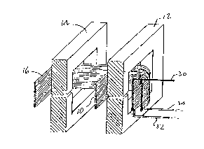
Figure 1 is an isometric view showing a compound inductor
assembly having two windings and two cores,
~ ~ 5 ~ 21472~
Figure 2 i8 an isometric view showing a compound
inductor as~et~ly having three winding~ and threo cores,
Figure 3 is a schematic diagram showing a buck
regulator circuit known in the prior art,
Figure 4 i~ a ~chematic diagram showing a soft
swi~ching buck regulator known in the prior art,
Figure 5 is a cutaway isometric view showing the
compound inductor assembly of Figure 1 with the air gaps
in the cores and the connections to the windings visible,
Figure 6 is a cutaway isometric view showing the
compound inductor assembly of Figure 2 with the air gap~
in the cores and the connections to the windings visible,
Figure 7 is a simplified schematic diagram showing a
compound inductor assembly according to one embodiment of
the present invention when the first winding has
substantially fewer turns than the second winding,
Figure 8 i8 a schematic diagram showing a compound
inductor assembly according to anotller embodiment of the
present invention when the first winding has the same
number of turns as the second winding,
Figure 9 is a schematic diagram showing a
simplification of the diagram of Figure 8,
Figure 10 is a schematic diagram showing the
compound inductor of Figure 9 in a two stage low pass
~ilter,
Figure 11 i~ a schematic diagram showing a compound
inductor assembly according to a further embodiment of
21~7~93
-- 6 --
the present invention when the first winding has slightly
more turns than the second winding,
Figure 12 is a schematic diagram showing a
simplification of the diagram of Figure 11,
Figure 13 i8 a schematic diagram showing the
compound inductor of Figure 12 in a two stage low pas~
filter with a resonant notch,
Figure 14 is a schematic diagram showing a
switch buck regulator with a compound inductor assembly
combining the inductor assemblies of Figure 7 and Pigure
8.
Modes for Carryinq Out the Invention
A compound inductor of the present invention has
asymmetrical coupled windings and multiple magnetic
cores. Figure 1 illustrates a first winding 10 on a
first magnetic core 12 and a second magnetic core 14
outside the first winding 10 and having a second winding
16 around the first winding 10 and the first core 12 and
also the second core 14. In this configuration the
deqree of magnetic flux coupling between the windings is
asymmetrical in the sense that virtually all of the flux
generated by a current in the first winding 10 i8
encompassed by the second winding 16, but only a portion
of the flux generated by a current in the second winding
16 is encompassed by the first winding 10.
A changing current in the first winding 10 generates
a corresponding change in the flux in the first core 12
which results in a voltage across the first winding 10
equal to the winding inductance times the rate of change
of current. A voltage is also generated on the second
winding 16 with the same "volts per turn" as the first
2147293 ,.-'~
winding 10 since the same flux is encompassed by both
windings.
A current in the second winding 16 produces a flux
in both the first core 12 and the ~econd core 14. Only
the flux in the first core 12 is encompassed by the first
winding 10, thus a changing current in the second winding
16 generates a lesser "volts per turn" on the first
winding 10 than on the second winding 16, as only a
portion of the total flux is encompassed by the first
winding 10. Thus, the flux coupling is termed
"asymmetric". Furthermore, the changing current flowing
in the first winding 10 and the second windinq 16 both
have the same polarity.
Figure 2 illustrates an extension to Figure 1 with a
third magnetic core 18 positioned outside the second
winding 16 and a third winding 20 which extends around
the first and second windings 10,16 and the first, second
and third cores 12,14,18.
Cores of transformers typically have high
permeability and are used to minimize energy storage and
excitation currents. Inductors in some embodiments are
designed to provide a high impedance to alternating
currents or to store energy. Inductors designed for
maximum impedance like transformers utilize high
permeability cores in order to maximize inductance.
Inductors designed for energy storage have cores of
moderate permeability. High permeability cores
magnetically saturate with relatively little current in
the winding, and the energy storage is low. ~owever, the
magnetic field in "air cored" inductors is low when the
winding is carrying the maximum current without over-
heating. This results in low energy storage.
2147293
-- 8 --
Maxlmum energy ~torage iB achieved with simultaneous
maximum winding current (a thermal limit) and core flux
den~ity (saturation or lo~s limited). This typically
requires cores with effective permeabilities between ten
and a few hundred, as opposed to unity for air and 1,000
to 100,000 for ungapped magnetic materials. These
intermediate permeabilities are achieved with one or more
discrete "air gaps" in a high permeability core, or with
a "di~tributed gap" material, o~ten referred to
generically as "powdered iron".
For the present invention, the compound inductor~
are of the energy storage type, the cores are of moderate
effective permeability utilizing one or more discrete air
gaps or a distributed gap material.
A basic schematic diagram of a prior art ~witching
buck regulator is sllown in Figure 3 and Figure 4.
Wherea~ a buck regulator is disclosed herein, it will be
understood that a buck regulator becomes a boost
regulator when active switche~ are replaced with diodes,
and diodes are replaced with active switches. Thus, the
direction of current and power flow i8 reversed. In the
case of Figure 3, the circuit becomes a boost regulator
when Sl and D1 are interchanged and in the case of Figure
4, the circuit becomes a boost regulator when S1 and S2
are interchanged with D1 and D2 respectively.
In the embodiment shown in Figure 7, the fir~t
winding 10 (pilot inductor) is tapped into the second
winding 16 (main inductor) of a soft switching regulator.
The connection~ are similar to that shown in Figure 5.
The fir~t winding 10 extends from a common connection
terminal 30 to the othex end terminal 32 of the first
winding 10. The second winding 16 extends from common
connector terminal 30 to the other end terminal 34 of the
second winding 16. The inductance Ll between terminals
/ ~;i~
. ~
214729~
g
30 and 34 shown in Figure 7 is the inductance of the
second winding 16 with the first winding 10 open
circuited. Thi8 is the same as the inductance of the
second winding 16 with both cores in place. The
effective inductance L2 in series with the tap is the
inductance observed between terminals 30 and 32 with the
second winding 16 short circuited and is typically less
than the inductance Ll.
This inductor arrangement i8 used in soft switching
buck and boost regulators of the type illustrated in
Figure 4. Switch S2, diode D2, and pilot inductor L2 are
added to a buck regulator of the type shown in Figure 3
as well as the usual capacitors Cl and C3. Closing S2 in
Figure 4 brings the voltage on switch S1 to zero before
S1 turns on, thus reducing switching losses. The energy
stored in L2 is returned to the output through D2 by
turning S2 off after S1 turns on.
The compound inductor of the present invention
reduces the total inductor size and power losses.
Inductor L2 operates with a high pulse current and core
flux and the attendant core and windinq losses may cause
a discrete inductor to be over sized and not much smaller
than Ll physically, although much smaller in inductance.
Utilizing part of the relatively large L1 core for L2
reduces the number of turns required for the pilot
inductance (first winding 10), and thus also reduce~ the
conductor losses due to the pulse current.
At the same time the pulse flux in the core is
reduced by the small number of pilot inductor turns
(first winding 10), which minimize the core loss. The
main inductor (second winding 16) typically generates
negligible core hysteresis loss due to the moderate AC
current component. The core flux is principally
saturation limited by the DC current plus half the peak-
21~7293 ('
_ -- 10 --
to-peak AC ripple current. The additional core 108~ due
to the pulse flux typically requires no increase in the
required main inductor core ~ize. Thus, total winding
and core losses are reduced in an assembly that is little
larger than L1 alone.
In another embodiment, the first and second ~tage
filter inductors of the switching requlator low pass
filter are combined in a single compound inductor
assembly in which the first and second inductor windings
have the same number of turn~. The configuration of this
embodiment is similar to that shown in Figures 1 and 5,
thus the voltages on the two windings are of the same
polarity. The circuit illustrated in Figure 8 shows the
common connection terminal 30 with the first winding 10
extending to connection terminal 32 and the second
winding 16 extending in two halves to connection terminal
34. The inductance L3 observed between terminals 30 and
32 is the inductance of the first winding 10 with the
second winding 16 open circuited. This is the same as
that of the first winding 10 and the first core alone.
The inductance L4 between terminals 32 and 34 i9 the
inductance of the second winding 16 with the first
winding 10 short circuited. This is the same as the
inductance of the second winding 16 and second core
alone.
The voltages on the two windings of inductance L3
are identical in this case, so inductance L4 is
effectively connected between terminal~ 32 and 34. The
equivalent circuit of Figure 8 may be replaced by the
simplified equivalent circuit of Figure 9.
Figure 10 shows the resultant equivalent of two
inductors in series as used in a two stage inductor
capacitor low pass filter. The second capacitor C2 may
not be essential. In the output of a buck regulator, AC
2147293
-- 11 --
ripple is ~iltered from a unipolar pulse voltage with the
average DC voltaqe at the output. This i~ illustrated in
the left and rigllt graphs of Figure 10. Virtually all of
the high frequency AC current f lows in the fir~t winding
10 from terminal 30 to terminal 32 and to a first
condense~ Cl while DC and low frequency currents flow in
the second winding 16 to tlle output terminal 34. Since
the first winding 10 carries only the AC ripple current,
a smalle~ wire gauge (or thinner foil) than the second
winding 16 can be used. The compound inductor may also
be used on the input of the buck regulator, or in the
input or output of boost or isolated regulator~ for
additional filtering.
The compound inductor shown in Figure 10 has
advantages over inductors with separate windings and
cores in that reduction in overall phy~ical size is
achieved and also reduction occurs in DC conductor losses
in the second winding 16. These advantages are both due
to the longer total winding length which would have to
wrap around the two cores individually if tlley were used
in the conventional and known type of inductors.
~ furtller embodiment a~ ShOWtl in Figure 11 i~
similar to tlle embodiment shown in Figure 8 except the
first winding 10 llas at least one more turn tllan tlle
second winding 16. The AC voltage on the second winding
16 is now slightly lower than on tlle first winding 10
which makes it appear that the second in~uctance L4 in
the equivalent circuit is connected to a tap on the firfit
inductance L3 as sl-own in Figure 12.
Wllen used in a low pas~ filter, the circuit of
Fiqure 13 results. The voltage between terminal 32 and
the tap of L3 i~ of opposite phase to the voltage on
capacitor C1. At some point above tlle low pa~ corne~
frequency, the voltages on the tap and Cl cancel,
- 12 _ 214729~
creating the effect of a re~onant notch in the
attenuation characteristic. This effect i 8 useful in
removing a strong undesirable fixed frequency component,
such as the fundamental frequency of the pulse input
voltage.
The advantage of the embodiment ~hown in Figure~ 11
to 13 are similar to those of the embodiment shown in
Figures 8 to 10 with the additional advantage of the
resonant notch in the high frequency attenuation.
~ still further embodiment i8 nhown in Figure 14
which combines the embodiment ~hown in Figures 8 to 10
and tlle e~bodiment ShOWtl in Figures 11 to 13, having
three winding~ and th~ee cores as illustrated in Figures
2 and 6. The common conrlection terminal 30 is shown
connecting througll the first winding 10 to the other end
terminal 32 througll the second winding 16 to tlle other
end terminal 34 and thro-lgh the third winding 20 to the
other end terminal 36. The first winding 10 has fewer
turns than the second winding 16, and the tllird winding
20 llas at least the same number o~ turns as the second
winding 16. ~ soft switching buck regulator utilizing
this embodiment is sllown in Figure 14. The main inductor
is Ll, the pilot inductor is L2 for soft switching, and
L4 is the second stage output filter inductor. The same
compound inductor can be used in a soft switching boost
regulator by exchanging the position~ of Sl and Dl and S2
with D2.
Various changes may be made to the embodiments shown
herein without departing from the scope of the present
invention which is limited only by the following claims.