Note: Descriptions are shown in the official language in which they were submitted.
93-AIL-336
214816.
MICROWAVE CROSSPOINT BLOCKING SWITCH MATRIX AND ASSEMBLY
EMPLOYING MULTILAYER STRIPLINE AND
$IN DIODE SWITCHING ELEMENTS
BACKGROUND OF THE INVENTION
Field of the Invention
This invention relates to switches for routing the
path an electronic signal travels, and more particularly
to blocking switch matrices for routing the path an
electronic signal travels from an input transmission line
to one of a series of output transmission lines within an
electronic circuit assembly.
Description of the Prior Art
Blocking switch matrices are well known in the
electronics industry. Present blocking switch matrices
are constructed in accordance with two approaches. The
first utilizes orthogonal three-dimensional arrangements
of transmission lines, directional couplers and solid
state switches that are fabricated and assembled using
Hybrid Microwave Integrated Circuitry (HMIC) techniques.
The second utilizes Monolithic Microwave Integrated
Circuitry (MMIC) techniques wherein crossed, non-
intersecting transmission lines, interconnections and
switch elements are integrated on a multilevel substrate
(chip) using semiconductor processing techniques.
Switching devices fabricated utilizing the MMIC
technique are preferable over switches made in accordance
with the HMIC technique because the MMIC switches are
smaller in size and, due to fewer welded interconnections,
have improved reliability. However, both the HMIC and
MMIC techniques suffer from drawbacks. Specifically, the
HMIC technique produces assemblies which are both bulky
2148161
_2_
and unreliable because of numerous welded
interconnections. In addition, the switch matrices
produced by the HMIC technique are relatively costly to
produce due to the significant amount of manual labor
required for assembly. The MMIC technique is impractical .
because chip size becomes very large due to the inherent
circuit complexity, even for low order switching matrices,
causing wafer yield to be low and therefore wafer cost to
be high. Finally, both techniques require the splicing of
input and output transmission lines for the insertion of
either the HI~IIC or MMIC switching devices which can
increase the time and cost required to produce such
devices.
OBJECTS AND SUMMARY OF THE INVENTION
It is an object of the present invention to provide a
blocking switch matrix and assembly for use with shielded
strip transmission lines.
It is another object of the present invention to
provide a blocking switch matrix which overcomes the
inherent disadvantages of known blocking switch matrices
and blocking switch matrix assemblies.
In accordance with one form of the present invention,
a microwave crosspoint blocking switch matrix assembly
includes at least a plurality of input microwave
transmission lines, a plurality of output microwave
transmission lines and a plurality of pin diode arrays.
The microwave crosspoint blocking switch matrix assembly
is capable of transmitting an input signal having a
specific wavelength (~,) or range of wavelengths from a
specific input transmission line to a selected output
transmission line. This passing of the input signal is
accomplished without severance of either transmission line
at their crosspoint and insertion of a series switch
214161
-3-
component, which switch component is required in a
conventional switch matrix.
A microwave crosspoint blocking switch matrix
assembly includes a plurality of input microwave
transmission lines selectively electrically coupled and
decoupled to a plurality of output microwave transmission
lines by a plurality of pin diode arrays. Each of the
plurality of pin diode arrays is attached to one input
transmission line and one output transmission line. Each
of the input and output transmission lines are preferably
spaced from adjacent respective input and output
transmission lines by
4~2N
where N is a positive integer or zero and .1 is the
wavelength of the input signal being transmitted.
However, the input transmission line can have a different
spacing (i.e., a different integer N) than the output
transmission line.
In a preferred form of the invention, each pin diode
array includes first and second connection points for
connection to corresponding input and output lines,
respectively, and first and second nodes. More
specifically, the first and second connection points of
each pin diode array are respectively coupled to one of
the plurality-of input microwave transmission lines and
one of the plurality of output microwave transmission
lines. The pin diode array also includes at least first,
second and third diodes wherein the cathode of the first
diode and the anode of the second diode are coupled to the
first node, the anode of the first diode and the cathode
of the third diode are coupled to the second node, and the
cathode of the second diode and the anode of the third
diode are coupled to ground potential. The pin diode
array also includes control lines coupled to the nodes and
on which are provided selectable biasing voltages to turn
2148161
,,"" _ 4 _
on or off individual diodes of each array. Each pin diode
array may also include at least one filter means coupled
between the first node and the first conrnection point for
blocking DC voltage from the control lines.
In accordance with another form of the present
invention, a microwave crosspoint blocking switch matrix
assembly includes at least a thin substrate supporting
base plate (also referred to as the first stratum) with a
first transmission line supporting stratum attached
thereto. The first stratum includes a bottom metallic
layer and a top dielectric layer with a plurality of first
transmission lines embedded within the top dielectric
layer. Each of the plurality of first transmission lines
are spaced from corresponding adjacent transmission lines
by
1
4~2A
where ~1 is the wavelength of the input signal provided to
the switch matrix assembly, and A is a positive integer or
zero.
Attached to the top dielectric layer of the first
stratum is an intermediate stratum composed of a bottom
layer of dielectric material and a top layer of metallic
material.
The assembly also includes a second transmission line
supporting stratum composed of dielectric material
attached to the top metallic layer of the intermediate
stratum, wherein the dielectric material of the second
stratum has a plurality of second transmission lines
embedded therein and spaced apart by
4~28
where B is a positive integer or zero.
214811
~.~. _ 5 _
Embedded within the microwave crosspoint blocking
switch matrix assembly are a plurality of pin diode arrays
for coupling one of the first transmission lines to one of
the second transmission lines. The assembly also includes
a top covering stratum composed of a dielectric layer and
a metallic layer superposed on the dielectric layer,
wherein the dielectric layer of the top covering stratum
is attached to the second stratum. The microwave
crosspoint blocking switch matrix assembly may also
include a plurality of cylindrical apertures adjacent to
each transmission line, formed through the assembly from
the metallic layer of the top covering stratum to the
metallic layer of the first stratum. The walls which form
each of the plurality of apertures are metal-plated so as
to electrically couple the metallic layer of the top
stratum to the metallic layer of the first stratum in
order to provide electrical isolation of each transmission
line from adjacent transmission lines.
A preferred form of the microwave crosspoint blocking
switch matrix assembly employing multilayer stripline and
pin diode switching elements, as well as other
embodiments, objects, features and advantages of this
invention, will be apparent from the following detailed
description of illustrative embodiments thereof, which is
to be read in connection with the accompanying drawings.
BRIEF DESCRIPTION OF THE DRAWINGS
Figure 1 is a block diagram of a microwave crosspoint
blocking switch matrix assembly formed in accordance with
the present invention.
Figure 2 is a functional block diagram of one form of
a microwave crosspoint blocking switch matrix formed in
accordance with the present invention.
2~4816~
.,. -6-
Figure 3 is a simplified schematic diagram of a
microwave crosspoint blocking switch matrix assembly
formed in accordance with the present invention.
Figure 4 is a perspective view of a preferred
arrangement of the microwave crosspoint blocking switch
matrix assembly employing multilayer stripline and pin
diode switching elements formed in accordance with the
present invention.
DETAILED DESCRIPTION OF THE PREFERRED EMBODIMENTS
Referring now to Figure 1 of the drawings, a
preferred form of a microwave crosspoint blocking switch
matrix assembly employing multilayer stripline and pin
diode switching elements constructed in accordance with
the present invention will now be described. The
microwave crosspoint blocking switch matrix assembly 1 is
designed to electrically couple and decouple input
microwave transmission lines to output microwave
transmission lines without requiring the severance of the
transmission lines and insertion of a series switch
element.
The microwave crosspoint blocking switch matrix
assembly 1 basically includes a plurality (X) of input
transmission lines 2, a plurality (Y) of output
transmission lines 4, and a plurality of pin diode arrays
6. Each of the plurality of pin diode arrays is coupled
to one input transmission line and one output transmission
line without duplication, so that the number of pin diode
arrays required for constructing a microwave crosspoint
blocking switch matrix assembly is substantially
equivalent to the number of input transmission lines
multiplied by the number of output transmission lines.
Preferably, the transmission lines utilized in the present
invention are shielded microwave stripline and the like.
2148~6~
.-
This type of transmission line provides a greater degree
of electrical isolation to each individual stripline than
unshielded transmission lines so that the signal being
transmitted will have a reduced likelihood of experiencing
electrical interference from neighboring transmission
lines. Adjacent input transmission lines, while aligned
in parallel, are preferably spaced a sufficient distance
from one another so as to avoid significant cross-
coupling. Likewise, adjacent output transmission lines
which are aligned in parallel are also spaced a sufficient
distance from one another in order to avoid significant
cross-coupling.
In a preferred embodiment of the present invention
and as shown in Figure 1, a pin diode array 6 is coupled
from each input transmission line 2 to each output
transmission line 4 at or near a crosspoint 8 of each
input and output transmission line. As shown in Figure 2,
the pin diode array 6 includes first and second connection
points 10,12 and first and second nodes 14,16. Proximate
to each crosspoint 8, connection point 12 is coupled to an
input transmission line and connection point 10 is coupled
to an output transmission line. The pin diode array 6
need not be coupled to each transmission line at the
precise crosspoint of the input and output transmission
lines. Instead, connection points of the pin diode array
6 need only be substantially proximate to the crosspoint 8
of the input and output transmission lines. It is
important to note that the transmission lines need not be
severed for insertion of the pin diode array as was
required for prior art switching matrices. Instead, the
pin diode array is coupled at its connection points 10,12
to the respective transmission lines 2,4 by ribbon-
bonding, soldering or by other suitable methods.
CA 02148161 2000-07-OS
_8_
As shown in Figure 2, each pin diode array 6 includes
at least first, second and third diodes 18,20,22. The
first diode 18 is connected between an input transmission
line 2 and an output transmission line 4 and is biased on
or off to selectively provide the interconnection of the
two transmission lines. The second and third diodes 20,22
are respectively connected between an output transmission
line 4 and ground and an input transmission line 2 and
ground. Each of the second and third diodes act as a
variable line termination by being selectively biased on
or off. Preferably, the cathode of the first diode 18 is
coupled to the first node 14 while the anode of the first
diode is coupled to the second node 16. Furthermore, the
anode of the second diode 20 is coupled to the first node
14 while the cathode of the third diode 22 is coupled to
the second node 16. Finally, the cathode of the second
diode 20 and anode of the third diode 22 are coupled to
ground potential. Of course, it should be realized that
the polarities of the diodes may be reversed with equal
results, as long as the proper biasing is applied.
Each pin diode array 6 includes a pair of control
lines 24,26 respectively coupled to nodes 14,16.
Selectable DC biasing voltages V (i.e., positive, negative
or zero voltages with respect to ground potential) are
provided on the control lines 24,26 of the array to
forward bias (turned on) or reverse bias (turned off) the
selected individual pin diodes of the arrays. Normally,
zero voltage is provided on the control lines of each pin
diode. As a result, the diodes of each pin diode array
are normally off so that there are no connections between
the input and output transmission lines. However, when a
signal is to be provided from an input transmission line
to an output transmission line, proper biasing voltages
are supplied for the duration of the connection.
2148161
°r.. _ 9 _
For example, a positive voltage on line 26 provided
to node 16 and, simultaneously, a negative or zero voltage
on line 24 provided to node 14 will forward bias (turn on)
the interconnecting diode (i.e., first diode 18) to the
conductive state. Diode 18 will thus appear as a short
circuit between the respective input and output
transmission lines 2,4 to which it is connected, thereby
interconnecting the two transmission lines to allow the
input signal to be transferred from the input transmission
line 2 to the output transmission line 4 controlled by
that particular pin diode array 6.
Alternatively, by simultaneously applying a negative
or zero voltage to control line 26 and a positive or zero
voltage to line 24, first diode 18 will be reverse biased
(turned off) so that the pin diode array 6 appears as an
open circuit between the respective input and output
transmission lines 2,4 to which the pin diode is
connected. In this state, the pin diode array 6 will
prevent the input signal from being transferred from input
transmission line 2 to output transmission line 4.
As for the termination diodes (i.e., second and third
diodes 20,22), a positive voltage on control line 24 will
forward bias diode 20, and a negative or zero voltage on
control line 24 will turn off diode 20 while a negative
voltage on control line 26 will turn on diode 22, and a
positive or zero voltage on line 26 will turn off diode
22.
The termination diodes 20,22 of two pin diode arrays
6, a first situated x/4 along an input transmission line
and a second situated .1/4 along an output transmission
line from a particular crosspoint 8 of the two
transmission lines to be switched, operate in conjunction
with the interconnecting diode 18 of the pin diode array
situated at the crosspoint. The interconnecting diode 18
CA 02148161 2000-07-OS
-10-
' ~ will selectively interconnect the input and output
transmission lines 2,4 to which it is connected when the
proper bias voltage is provided to the diode 18 on control
lines 24,26. Simultaneously, the second diode 20
connected to the selected output transmission line and
situated 1/4 away from the crosspoint of the two
transmission lines in a second pin diode array is forward
biased by providing a sufficient biasing voltage on
control line 24 of the second array (containing the second
diode 20). In addition, the third diode 22 connected to
the selected input transmission line and situated 1/4 away
from the crosspoint in a third pin diode array is forward
biased by providing a sufficient biasing voltage on
control line 26 of the third pin diode array (containing
the third diode). The two termination diodes 20,22, being
forward biased, appear as short circuits in their
respective pin diode arrays, but appear as open circuits
1/4 away at the crosspoint of the input and output
transmission lines being coupled together by
interconnection diode 18. Accordingly, at the respective
crosspoint, the signal transferred from the input
transmission line 2 to the output transmission line 4 sees
a high impedance on the transmission lines and is
therefore not loaded down or attenuated.
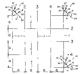
Referring now to Figure 3, an example of how the
microwave crosspoint blocking switch matrix of the present
invention operates will be described. Figure 3
illustrates a 5 x 5 blocking switch matrix array having
five input transmission lines 2 numbered #1-5 and five
output transmission lines 4 numbered #1-5 wherein an input
signal (having a wavelength ~ or range of wavelengths) is
provided on input transmission line number #5 and
thereafter provided on output transmission line number #1.
Preferably, each input transmission line 2 is spaced 1/16
apart (shown if Figure 3 as dimension "a") from adjacent
input transmission lines 2. Likewise, each output
2I~$1~~
... -11-
transmission line 4 is spaced .1/16 apart (shown in Figure
3 as dimension "a") from adjacent output transmission
lines 4. However, the adjacent input and output
transmission lines can be spaced apart by any distance
derived from the mathematical relationship:
4~2~
where N is a positive integer or zero. It should be noted
that the integer N that is used for deriving the required
spacing of the input transmission lines 2 can be different
than the integer N used for the spacing of the output
transmission lines 4. As described above, and for the
purposes of illustration, input transmission line number 5
and output transmission line number 1 are the respective
input and output transmission lines utilized for the
example of the operation of the microwave crosspoint
blocking switch matrix.
The microwave crosspoint blocking switch matrix of
Figure 3 preferably includes a plurality of pin diode
arrays 6 (however, only three pin diode arrays 28,30,32
are shown) respectively coupling each input microwave
transmission line 2 to each output microwave transmission
line 4 without duplication. The pin diode arrays are
preferably placed at or near a crosspoint 8 of respective
input and output microwave transmission lines. Based upon
the selected input transmission line and output
transmission line (i.e., input microwave transmission line
number #5 and output microwave transmission line number
#1), specific diodes 18,20,22 of specific pin diode arrays
will be activated to provide transmission of the signal
from the input microwave transmission line number #5 to
the selected output microwave transmission line number #1.
In order to provide the input transmission signal
from input transmission line number #5 to output
transmission line number #1, pin diode array 28 (having
first, second and third diodes 18,20,22 and control lines
CA 02148161 2000-07-OS
-12-
' ~ 24,26) located at the crosspoint of input transmission
line number #5 and output transmission line number #1 must
be activated. More specifically, pin diode array 28
includes an interconnecting diode 18 coupled between input
transmission line number #5 and output transmission line
number #l. The interconnecting diode 18 is selectively
biased on and off to couple and decouple input
transmission line number #5 and output transmission line
#1. The pin diode array 28 also includes second and third
diodes 20,22 respectively coupled between the output
transmission line number #1 and ground and the input
transmission line number #5 and ground, which act as
variable line terminations by selectively being biased on
or off.
As stated above, pin diode array 28 includes control
lines 24,26 respectively coupled to nodes 14,16. The
first, second and third diodes 18,20,22 of pin diode array
28 are normally off with zero voltage provided on control
lines 24,26. Selectable DC biasing voltages V (i.e.,
positive, negative or zero voltages with respect to ground
potential) are provided on the control lines 24,26 of pin
diode array 28 to forward bias (turn on) and reverse bias
(turn off) specific diodes.
Specifically, in order to activate interconnecting
diode 18 of pin diode array 28 (first diode 18), a
positive voltage is provided on control line 26 to node 16
of pin diode array 28, and, simultaneously, a negative or
zero voltage is provided on line 24 to node 14 of pin
diode array 28. Thus, the interconnecting diode 18 of pin
diode array 28 (first diode 18) will be forward biased and
thus appear as a short circuit between input transmission
line number #5 and output transmission line number #l,
thereby interconnecting the two transmission lines.
CA 02148161 2000-07-OS
-13-
' ~ In addition to activating the interconnecting diode
(first diode 18) of pin diode array 28, specific
termination diodes (i.e., second and third diodes 20,22)
located at specific input transmission line 2 and output
transmission line 4 crosspoints must also be activated to
properly route the input signal from input transmission
line number #5 to output transmission line number #1.
Specifically, the pin diode arrays that are located in
directions that it is not desired to have the input signal
travel and which are located ~/4 (or any multiple thereof,
i.e., 3~/4, 5~/4...) from pin diode array 28 are
activated.
In view of the above and having elected to provide an
input signal from input transmission line number #5 to
output transmission line number #1, pin diode arrays
30,32, which are respectively located ~/4 along the input
transmission line number #5 and output transmission line
number #1 and which are located in directions of desired
non-transmission of the input signal are activated to
effectively block the transmission of the input signal in
the direction of location of the respective pin diode
arrays 30,32.
The termination diodes (diodes 20,22) of pin diode
arrays 30,32 situated ~/4 away from the crosspoint of
input transmission line number 5 and output transmission
line 1 are activated as follows. A positive voltage on
control line 24 of pin diode array 32 will forward bias
second diode 20 connected to selected output transmission
line number 1. In addition, third diode 22 of pin diode
array 30 will be forward biased by providing a negative
voltage on control line 26 of pin diode array 30. The two
termination diodes (second diode 20 at pin diode array 32
and third diode 22 of pin diode array 30) being forward
biased, appear as short circuits in their respective pin
diode arrays 30,32, but appear as open circuits ~/4 away
CA 02148161 2000-07-OS
-14-
' ' at the crosspoint of the input transmission line number 5
and output transmission line number 1. Accordingly, the
signal provided on input transmission line number 5 sees a
high impedance on the input and output transmission lines
at the crosspoint and is therefore not loaded down or
attenuated. As a result, substantially complete
transmission of the input signal from a selected input
transmission line to a selected output transmission line
can occur without utilizing and inserting a service
switching component. It should be noted that more than
one combination of input transmission lines and output
transmission lines may be simultaneously switched in the
microwave crosspoint block switch matrix assembly of the
present invention. Therefore, respective input signals
may be provided on adjacent input transmission lines and
transferred to adjacent output transmission lines by
forward biasing selected diodes of pin diode arrays of the
switch matrix assembly.
Returning again to Figure 2 of the drawings, in a
preferred embodiment of the present invention, each pin
diode array 6 may further include first filter means 34
coupled between the first connection point 10 and first
node 14, and second filter means 36 coupled between the
second connection point 12 and the second node 16. The
first and second filter means 34,36 preferably include at
least one capacitor for blocking DC voltage provided to
control lines 24,26 in order to electrically isolate the
pin diode array 6 from the transmission lines and the
circuit to which each pin diode array is coupled. The pin
diode array 6 may also include first and second decoupling
filter circuits 38,40 interposed in and coupled to the
control lines 24,26 respectively. Each decoupling filter
circuit 38,40 preferably includes at least one inductor 42
and one capacitor 44 connected in parallel so as to form
35. an LC filter circuit.
. 2148161
-15-
One form of a crosspoint switch matrix assembly of
the present invention is shown in Figure 4 wherein the
microwave crosspoint blocking switch matrix assembly is
designed for providing an input signal having a specific
wavelength (~1), or range of wavelengths, from an input
transmission line 2 to an output transmission line 4. The
microwave crosspoint blocking switch matrix assembly shown
in Figure 4 basically includes a thin substrate supporting
base plate 46 which is preferably constructed from a
metallic conductive material. Attached to the top of the
base plate 46 is a first transmission line supporting
stratum 48 which includes a bottom metallic layer 50
affixed to the base plate 46, and a top dielectric layer
52. The dielectric layer preferably has a plurality of
shielded transmission lines 54 embedded therein or formed
on its surface. Adjacent transmission lines are
preferably spaced apart by
4~2A
where A is either a positive integer or zero and ~1 is the
wavelength of the input signal. In a preferred embodiment
of the invention, adjacent transmission lines are spaced
X1/16 apart. Preferably, the layers of the first stratum
48, specifically the dielectric and metallic layers 52,50,
have a substantially uniform thickness over their entire
length and width.
Attached to the dielectric layer 52 of the first
transmission line supporting stratum 48 is an intermediate
stratum 56 which preferably includes a bottom dielectric
layer 58 and a top metallic layer 60. Preferably, the
dielectric layer 58 of the intermediate stratum 56 is
affixed to the dielectric layer 52 of the first
transmission line supporting stratum 48. The intermediate
stratum 56, with its metallic layer 60, is designed to
provide electrical isolation of the transmission lines 54
formed in the first transmission line supporting stratum
48. Preferably, both the dielectric layer 58 and metallic
CA 02148161 2000-07-OS
-16-
layer 60 of the intermediate stratum 56 have a
substantially uniform thickness over their entire length
and width.
Attached to the intermediate stratum 56 is a second
transmission line supporting stratum 62 which is
preferably made of a dielectric material 64 having a
plurality of transmission lines 66 embedded therein (or
formed on one of its surfaces). The transmission lines 66
may be stripline or cylindrical conductor. Adjacent
transmission lines 66 are preferably spaced apart by
1
4 ~~
where B is either a positive integer or zero and ~ is the
wavelength of the input signal. In a preferred embodiment
of the invention, adjacent transmission lines 66 are
spaced .1/16 apart. The B chosen for the spacing of the
second transmission line need not be the same as the A
chosen for the spacing of the first transmission lines.
Furthermore, the dielectric layer of the intermediate
stratum preferably has a substantially uniform thickness
over its entire area. The transmission lines 54,66 of the
first and second supporting strata 48,62 may function as
either input transmission lines 2 or output transmission
lines 4 (See Figure 1).
The microwave crosspoint blocking switch matrix
assembly further includes a plurality of pin diode arrays
6 preferably embedded within at least one of the first
transmission line supporting stratum 48, the intermediate
stratum 56 and the second transmission line supporting
stratum 62. The pin diode arrays 6, each having two
connection points 10,12, are preferably located at each
crosspoint of the transmission lines 54,66. The two
connection points 10,12 of the pin diode arrays 6 are
respectively coupled to the transmission lines 54,66
proximate to each crosspoint. The pin diode arrays 6 are
inserted in the assembly by drilling or otherwise forming
CA 02148161 2000-07-OS
-17-
' ' an aperture 68 in the assembly, and placing the pin diode
array 6 therein. Thereafter, the pin diode array 6 is
electrically connected to the transmission lines 54,66 at
its connection points 10,12 proximate to the crosspoint of
the transmission lines by conductive strip 55,67
respectively.
The microwave crosspoint blocking switch matrix
assembly further includes a top covering stratum 70 which
is attached to the top of the second transmission line
supporting stratum 62. The top covering stratum 70
includes a bottom dielectric layer 72 and a top metallic
layer 74 wherein the dielectric layer 72 of the top
covering stratum 70 preferably lies adjacent to the
dielectric layer 64 of the second transmission line
supporting stratum 64.
In a preferred embodiment, the assembly further
includes a plurality of apertures 76 (commonly called via
holes), each defined by an aperture wall formed from a
portion of the first transmission line supporting stratum
48, the intermediate stratum 56 and the second
transmission line supporting stratum 62. Preferably, the
via holes 76 are formed in the assembly after the first
stratum 48, intermediate stratum 56, and second stratum 62
are layered upon the base plate 46. Thereafter, the top
covering stratum 70 is attached to second stratum 62. The
via holes can be formed by any known means for forming a
hole through the dielectric and metallic layers such as by
drilling to remove only the required material. The via
holes 76 are formed through the assembly and are preferably
adjacent to a corresponding transmission line as shown in
Figure 3. More specifically, the via holes are spaced
apart from each other in parallel rows on each side of a
transmission line. The spacing between via holes is
selected in a well known manner to provide electrical
isolation between the transmission lines.
CA 02148161 2000-07-OS
-18-
Once the via holes 76 have been formed, each via hole
wall is plated with a metallic material by any suitable
method. The via holes 76 serve several purposes.
Firstly, the via holes serve to couple each metallic layer
of the various strata to the metal base plate 46 in order
to have a common reference ground. Secondly, the via
holes 76 serve to electrically isolate each transmission
line 54,66 from adjacent respective transmission lines so
as to minimize cross coupling and interference between the
transmission lines. Finally, the control lines 24,26 (as
previously described with regard to Figures 2 and 3) may
be passed thru the via holes to their respective pin diode
arrays 6 for selectively biasing the first, second and
third diodes 18,20,22.
In an alternate embodiment of the present invention,
the entire microwave crosspoint blocking switch matrix
assembly further includes a ceramic or other non-
conductive coating 78 (partially shown in Figure 4) around
the entire assembly for hermetic sealing of the device so
that the assembly will be impervious to environmental
effects such as dust, dirt and corrosive elements.
It should be noted that although the matrix is
particularly suited for use with pin diodes, other
devices, such as microwave switches, exhibiting an on
(short circuit) and off (open circuit) state may be used
in place of the pin diodes. As a result of the present
invention, the transfer of a signal from an input
transmission line to an output transmission line is
accomplished without the insertion of a series switch
component by severance of either transmission line at the
respective crosspoint, which switch component is required
in conventional switch matrices.
~~4816~
'~ -19-
Although illustrative embodiments of the present
invention have been described herein with reference to the
accompanying drawings, it is to be understood that the
invention is not limited to the precise embodiments, and
that various other changes and modifications may be
effected therein by one skilled in the art without
departing from the scope or spirit of the invention.