Note: Descriptions are shown in the official language in which they were submitted.
2148178
"T~LEPI~ONE LI~E SOURC~D POr~R SUPPLY"
The invention relates to low-power power supplies,
and more particularly to low-power power supplies
capturing power from a telephone line.
Mobile computers, particularly laptop computers
and notebook computers, have become increasingly
popular. They have performance and capabilities near
that of a desktop unit, and if color active matrix
liquid crystal displays are utilized, the display is as
good as a desktop unit. When combined with the
mobility, the popularity is quite underst~n~Ahle.
However, one problem with using portable computers is
that often they need to be connected to various
equipment. For example, when located in a office, it
is desirable to connect to various office wide items or
non-portable items. For example, a network interface
is often n~r~Cc~ry~ as is a SCSI port for use with
various external devices such as CD-ROMs. This
situation has conventionally been handled using
eYp~ncion bases, which contain expansion cards for
network and SCSI use and connections for a video
monitor, a printer and a full size keyboard, or port
replicator strips, which are used to simply provide the
connections to the monitor, printer and keyboard
without the need for exr~sion cards.
One of the computer applications which is becoming
prevalent is electronic mail or E-mail. The modern
- 21~8178
business often has a local area network (LAN), with E-
ma~1 and appointment calendar applications. A remote
u er, such as the laptop user away from the office
needs to check periodically to maintain in full
contact. Thus, a very common addition to a portable
computer is a modem to allow remote access to the LAN
or other dial up services. Typically this modem is
installed in the laptop computer, not directly in any
~xr~nSion base. So while an eYrA~ion base or port
replicator may alleviate certain wiring problems, as
the various cables need not be disconnected or
~.,octed when removing or installing the portable
computer, it does not resolve the wiring concerns in
the case of a modem, where a separate telephone line is
still required to be plugged and unplugged into-the
modem in the computer. This results in aggravation for
the user. Further, this telephone line is yet another
of the tangled mass of cables utilized with the modern
computer. While the monitor, keyboard and SCSI cables
are generally located right next to the co~ u~er to
interconnect the various components, the telephone line
often has to be ~LUll~ across an office and thus is
either unsightly or very difficult to route. This is a
further drawback to stAn~rd conventional modem
communications where the modem is contained in the
personal computer, be it a laptop or a desktop unit.
Thus the use of a modem in a laptop computer
results in aggravations for the user and additionally
requires unsightly and cumbersome cabling. Therefore
it is clearly desirable to simplify both the laptop
portability concerns and the unsightly wiring problem.
one solution to this problem is a cordless modem system
where a mobile station unit (MSU) is located in the
computer or connected to the computer and a base
station unit (BSU) which is con~ected to the telephone
7~
--3--
line. A radio frequency (RF) link is developed between the two
units to allow a cordless connection between the computer and
the telephone line. Such a system is further disclosed in
Canadian File No. 2,148,179 filed April 28, 1995 and has been
commonly assigned to the assignee of the present application.
Yet another extraneous cable would conventionally be
present in such systems, however. The BSU would typically be
powered by connection to a wall outlet, thus requiring both the
connection to that outlet as well as connection to the telephone
line. It would be greatly desirable if such a BSU and other
telephone line interface equipment did not require connection to
a wall outlet for power, thereby reducing the number of cables
and greatly simplifying installation of the sSU.
According to one embodiment of the invention, a
telecommunication unit requiring power even when on-hook is
powered using a charge storage device such as a capacitor. When
the unit is on-hook, power is received from the capacitor. When
the capacitor charge becomes too low, the unit goes off-hook for
a brief period of time to recharge the capacitor. When the
capacitor is sufficiently charged, the unit returns to normal
operation. The unit remains functional even while the capacitor
is being charged.
The invention in one aspect pertains to a power supply for
a device with circuitry requiring a supply voltage of a
generally constant voltage, the device connectable to a
telephone line and the circuitry including logic for indicating
the device is requesting to be taken off-hook. The power supply
includes means for providing the supply voltage to the
circuitry, the supply voltage means including a power input, a
capacitor for providing power to the power input of the supply
voltage means, a voltage being present across the capacitor,
means for providing voltage from the telephone line to the
capacitor when the device is off-hook, means for determining
when the voltage across the capacitor falls below a first
predetermined threshold and off-hook circuitry for forcing the
device off-hook responsive to the means for determining when the
voltage across the capacitor has fallen below the first
-3A- 2 ~ 7 ~ -
predetermined threshold.
A further aspect of the invention provides an electrical
device for communicating data over a telephone line and over a
radio frequency channel, comprising circuitry for communicating
data over the telephone line and the radio frequency channel,
the circuitry requiring a supply voltage of a generally constant
voltage and the circuitry including logic for indicating the
device is requesting to be taken off-hook. Means is provided to
supply voltage to the circuitry, the supply voltage means
including a power input and a capacitor provides power to the
power input of the supply voltage means, a voltage being present
across the capacitor. Means provides voltage from the telephone
line to the capacitor when the device is off-hook and means
determine when the voltage across the capacitor falls below a
first predetermined threshold. Off-hook circuitry forces the
device off-hook responsive to the means for determining when
the voltage across the capacitor has fallen below the first
predetermined threshold.
A
21~8178
-4-
According to a further emhoAiment of the
i~vention, a telecommunication unit is a base station
unit used in a cordless base station-mobile station
modem communication system.
Accordinq to yet another emhoAiment of the
invention, the period in which the unit is taken off-
hook is periodically interrupted to place the teleFhone
b~ck on-hook, even when the capacitor charge has not
been restored. This is done to prevent the telephone
system from perceiving the telephone line as being
connected to a telephone that has been unintendedly
left off-hook.
In one embodiment of the invention, the capacitor
charge is restored using a voltage regulator which
determines when a supply voltage has dropped below a
predetermined level. The voltage regulator then causes
a comparator to provide a low power indication signal.
The comparator reverts to its normal state once the
capacitor charge has been replenished to a
predetermined level.
According to yet a further embodiment of the
invention, the low power signal provided by the
comparator is further provided to a microcontroller,
which uses its processing capabilities to effectuate
t~king the telepho~ off-hook.
According to yet another embodiment of the
invention, a dial tone signal detected by a DTMF
controller is used to determine when the telephone has
been off-hook so long that the dial tone is lost. When
this occurs, either a monostable multivibrator is
triggered forcing the unit back on-hook for a brief
period of time, or the microcontroller performs the
same function.
21~8~7~
A better unders~n~in~ of the present invention
can be obtained when the following detailed description
of the preferred embodiment is considered in
conjunction with the following drawings, in which:
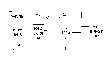
Figure 1 is a block diagram showing the computer,
cordless conn~ction and telephon~ jack in which the
present invention would typically be implemented;
Figure 2 is a block diagram of the base station
unit of Figure l;
Figure 3 is a schematic diagram illustrating the
off-hook circuitry used in the base station unit of
Figure 1;
Figure 4 is a schematic diagram of the power
supply circuitry used in the base station unit of
Figure l;
Figure 5 is a schematio diagram of circuitry used
to periodically place the unit on-hook in combination
with the circuitry illustrated in Figure 4;
Figures 6A and 6B are schematic diagrams of
alternative circuitry that may be used in conjunction
with the circuitry illustrated in Figure S;
Figure 7 is a flowchart illustration of an
interrupt routine that would be implemented in a
microcontroller as illustrated in Figure 2;
Figure 8 is a schematic diagram of circuitry
similar to that shown in Figure 5, but instead
employing a dial tone signal to trigger a monostable
multivibrator; and
Figure 9 is a flowchart illustration of an
interrupt routine similar to that shown in Figure 7,
but again employing a dial tone signal instead of a
timeout loop.
- 2148178
Referring now to Figure 1, the basic arrangement
of the compon~nts in which the present invention would
typically be implemented is shown. A computer system
C/ preferably a laptop or not~hoo~ computer but
optionally a desktop computer, contains an internal
modem M which is ronnPcted to a mobile station unit
(MSU) 1. The MSU 1 includes an antenna 400. A
telephone wall jack J is connected to telephone land
line. A base station unit (BSU) 2 is connected to the
teler~one jack J and also includes an antenna 402. A
radio frequency (RF) link is established between the
MSU 1 and the BSU 2 to pass information between the
computer C and the telephone jack J. The MSU 1
contains a serialized identification number, preferably
24 bits long, as does the BSU 2. This allows the MSU 1
to have a unique identity to allow security of
communications. Similarly, the BSU 2 also has this
identification to allow a secure link to be
established. The MSU 1 is connected to the internal
modem M by several alternate connections. In a first
embodiment the MSU 1 is configured as an external data
access arrangement (DAA) and is connected to an
external DAA port of the internal modem M. In this
emho~iment the MSU 1 is contained in a small box or
case. In an alternate embodiment the MSU 1 and the
internal modem M are combined into a single unit,
preferably in a PCMCIA form factor. The BSU 2 is
connected only to the telephone jack J and is not
otherwise powered but receives power from the telephone
line. This is further described below in conjunction
with Figures 3-7. The BSU 2 is contained in a small
box or case. The details of the MSU 1 and the BSU 2
are provided below.
21~8178
-7-
The circuitry and methods according to the
invention would typically be implemented in the BSU 2,
as will be ~ccl~c~ed below in conjunction with the
remaining Figures.
Referring now to Figure 2, the block diagram of
the BSU 2 is shown. An RJ 45 connector 11 is provided
in the BSU 2 to con~ect a data access arrangement (DAA)
422 to a teleF~o~e line. The DAA 422 is ~o~nected to a
transmitter 426, a receiver 428, and microcontroller
430, a DTMF decoder/encoder 432, and a power supply
434. The power supply 434 is connected to the DAA 422
to receive power from the telephone line and to provide
the proper voltages for operation of the BSU 2. The
microcGllL~oller 430, preferably the 68HC05 from
Motorola, operates as the control point for the BSU 2.
A DTMF d~coAer/encoder 432 is provided to allow
signaling and dialing if n~C~scary. An RF transmitter
426 is connected to properly frequency modulate the
received audio signal and provide it to an antenna 436.
The transmitter 426 is controlled by the
microcontroller 430. A receiver 428 is connected to
the microcol,~roller 430 and the antenna 436 to receive
the RF signal from the MSU 1 and provide the audio
signal to the DAA 422. The receiver 428 is similarly
controlled by the microcontroller 430.
In this description an asterisk suffix is used to
indicate a negative logic signal which is active when
as6erted low. The signal name without the asterisk
means that it is the inverse of that signal with the
asterisk.
Now the co~nections between the blocks will be
described in more detail. The DAA 422 contains the
necessary interface between the telephone line TIP and
RING signals which it receives as inputs and the
various other signals in the base station BSU 2. The
2148178
-8-
TIP and RING signals are provided to the power supply
434 to allow the base station BSU 2 to be entirely
powered by the teler~on~ line, as is further described
below in conjunction with Figures 3-7. The power
supply 434 provides the desired 3 volt signal and
transmitter 426 and receiver 428 voltages as n~c~cs~ry.
The DAA 422 includes a two wire to four wire conversion
to develop the RX signal and utilize the TX signal as
i~ ~onvellLionally known. Details of this conversion
are not included but an example is illustrated in U.S.
Patent No. 5,127,046, which is hereby incorporated by
reference. In the DAA 422, the FSK TX and DTMF TX
s;~n~ls are utilized and combined with the audio signal
received from the two to four wire converter to provide
the AUDIO TX signal. The AUDIO EN* signal is used to
clamp or disable the audio signal from the two to four
wire converter and AUDIO RX signals so that the
microconL~oller 430 can properly communicate with the
MSU 1 during command operations. A RING IND signal
provided from the DAA 422 to the microcontroller 430
provides a ring detection indication which can be
transmitted via a command to the NSU 1. The OFF HOOK*
signal is provided from the power supply 434 to the DAA
422 and is a combination of a VCC TX_EN signal and a
signal indicating that the power supply 434 needs
recharged. Basically the power supply 434 includes a
very large capacitor which is utilized to power the BSU
2 and the capacitor needs periodic recharging from the
DC voltage present on the telephone line. When
recharging is nececs~ry, the power supply 434 causes
the 8SU 2 to go off-hook to charge the capacitor.
Thus, the OFF HOOK* signal is developed either by the
power supply 434 for charging or by the microcontroller
430 when communications are desired based on the
2148178
VCC TX EN signal. This operation is described in
further detail below in conjunction with Figures 3-7.
The power supply 434 provides a 3 volt o~-~u~ for
operation of the circuitry of the preferred embodiment,
to save power, and provides VCC TX and VCC RX signals
w~ich provide power to the transmitter 426 and the
receiver 428 so that they can be completely powered
down when not in operation. To that end, the VCC TX EN
and VCC RX EN signals are received from the
microcontroller 430 to ~G~.L.ol or enable the VCC TX and
VCC RX o~L~uLs. The power supply 434 also provides the
RESET* signal to the microcontroller 430 to reset the
operation of the BSU 2 when the power supply is
inadequate. In one embodiment, the power supply 434
al o provides an INTA* signal to the microcontroller
430. This signal is coupled with the power supply's
low power logic, and provides an interrupt to the
microcontroller 430 indicating the on-hook storage
capacitor needs to be recharged. Similarly, two
control lines, PAx and PAy are provided between the
power supply 434 and the microcontroller 430. As is
di~cussed below in conjunction with Figures 6A and 6B,
these signals are further used to allow the
microcontroller 430 to control the recharging of the
storage capacitor in the power supply 434.
The DTMF decoder/encoder 432 provides the DTMF TX
ou~u~, which is used if dial tones are desired, and
receives the AUDIO RX signal from the receiver 428 to
allow decoding of any received DTMF signals. The DTMF
A~qco~er/encoder 432 is connected to the microcontroller
430 through data and control signals so that the
~sco~Pr/encoder 432 can interrupt the microcontroller
430 when a detected DTMF code is received and can
provide a bi-directional data and control port.
Further, the DTMF ~ecoAer/encoder 432 also preferably
2 1 ~ 8
--10--
provides a DIAL_TONE signal to the mic~G~ul.Lroller 430,
the POWER SUPP~Y 434, or both, to facilitate the use of
c~rcuitry and routines described below in conjunction
w~th Figures 8 and 9.
The transmitter 426 includes a radio frequency
rh~c~-locked loop (PLL) synthesizer (not shown) which
includes a serial interface. The PLL receives command
and setup data from a serial data link comprised of the
signals MOSI, MISO and SCK from the microcontroller
426. The SCK signal is the clock signal while the
other two signals are for the data input and data
u~L~uL. The serial interface allows the
microcontroller 430 to properly program the PLL
contained in the transmitter 426 to the desired
frequency of channel 1 or channel 2. The output of the
PLL is then provided to appropriate mixing circuitry to
mix in the AUDIO TX signal to produce the RF TX signal,
which is provided to the antenna 436. The antenna 436
can either be an integrated antenna or a short external
antenna. Additionally, the microcontroller 430
provides the TX RF EN and TX PLL EN signals to the
transmitter 426. The TX PLL EN signal is used to
enable or disable the PLL when desired, while the
TX RF EN signal disables the actual GuL~u~ of the
transmitter 426 which is provided to the antenna 436.
This allows the PLL to be activated or turned on in
preparation for a transmission which is to occur.
The receiver 428 includes a similar PLL,
preferably the MC145170 from Motorola Semiconductor.
The receiver 428 includes the MOSI, MISO and SCK
signals. The receiver 428 receives the VCC RX signal
from the power supply 434 to allow it to be completely
powered down. An RX PLL EN signal is provided from the
microcontroller 430 to receiver 428 to disable the PLL
in the receiver 428. The receiver 428 also includes a
21~8178
--11--
m~xer FM IF ~ystem, preferably t'he NE/SA606 from
p~ Semi~Q~ stor. The mixer FM IF system
receives an RF RX ~ignal from the antenna 436 and
~o~eLly mixes out the ch~nnel receive frequency so
that only the received audio data is present. This is
provided as the AUDIO RX signal to the DTMF
A~ r/e~o~Pr 432 and the DAA 422. An FSK RX signal
is a buffered version of the AUDIO RX signal and is
provided to a serial input of the microcontroller 430.
Thus the FSK TX and FSK RX signals are serial output
and input of the microcontroller 430. This serial
interface of the microcontroller 430 is the command
interface with the MSU 1. Preferably the serial
interface operates at a low speed, such as 1200 or 2400
b~ud. The receiver 428 also provides an RSSI or
receive signal indication to the microcontroller 430 to
indicate that the carrier is being received from a
MSU 1 and that a channel is active. This allows the
BSU 2 to monitor for a received signal indicating that
a given channel is busy.
Thus the BSU 2 provides the capability to receive
analog audio data from the telephone line and provide
it over an FM modulated RF link to the base station MSU
1 and to similarly receive an RF signal from the MSU 1
and decode the signal to provide an analog signal to
the telephone line. The microcontroller 430 provides
tbe control function which is needed for the DAA 434
and allows command passing between the BSU 2 and MSU 1.
Referring now to Figure 3, circuitry illustrating
the telephone line interface in the DAA 422, as well as
the circuitry for taking the BSU 2 off-hook, are shown.
The telephone line is provided through the RJll
connector 424, which provides st~n~rd TIP and RING
lines for communications. The signals on these lines
are well known in the art, but to review, from a 48
~ 2i48178
-12-
volt DC wire loop, which when c~nnected to data access
arrangement circuitry, result~ in the BSU 2 being taken
~off-hook.~ Ringing is indicated by an approximately
85 volt, 20 Hz signal superimposed on the 48 volt
slgnal. These are st~ rd values for the telephone
line operation and numerous variations are known, such
as a 24 volt PBX system. In all cases, a DC voltage is
present on the TIP and RING lines, and closing the loop
results in an off-hook condition.
A transorb 500 is provided across the TIP and RING
lines to clamp voltage spikes. After being filtered
through inductors 502 and 504, the signals on the TIP
and RING lines are then provided to a rectifier bridge
formed by rectifier diodes 506, 508, 510 and 512. The
cathodes of the rectifier diodes 506 and 508 are
connected to provide the rectified high signal from the
telephone line, while the anodes of the rectifier
diodes S10 and 512 are connected to provide a low
reference level from the telephone line. The RING
line, as filtered through the inductor 502, is provided
as a RING signal and is further provided through a
capacitor 514 to a transformer 516. This transformer
couples to stAn~Ard DAA circuitry 518, which
communicates over the telephone line. The signal on
the TIP line, as filtered through the inductor 504, is
further provided to the input of a solid state relay
520. The ou~u~ of the solid state relay 520 is
provided as a TIP signal and is further provided
through a capacitor 522 to the other side of the
transformer 516 as the TIP signal.
The solid state relay 520 turns on when an
appropriate voltage drop is developed across its VCC
and EN* inputs. When so energized, the solid state
relay 520 effectively couples the DAA circuitry 518 to
the telephone line, thus taking the BSU 2 off-hook.
21~8178
-
-13-
The circuitry used to take the BSU 2 off-hook is
activated by an OFF HOOK* signal, provided as an input
to an opto-isolated switch 524. The cathode of the
llght emitting diode in the opto-isolated switch 524 is
cQ~ected to ~L~u..d through a current limiting resistor
526. The light emitting diode acts on a photo-diode in
the base loop of a Darlington transistor pair so that
when the light emitting diode is active, the transistor
pair is saturated. Thus, when OFF HOOK* goes true, or
active low, the opto-isolated switch 524 becomes an
open circuit, whereas when OFF_HOOK* goes false, or
high, it becomes an effective short circuit.
The emitter and collector of the transistor pair
in the opto-isolated switch 524 are clamped by a Zener
dlode 527, thus limiting the emitter-collector drop.
The collector of the opto-isolated switch 524 is
further connected to one terminal of a pull-down
resistor 528, to the source of an N-channel MOSFET 530,
and to the rectified low side of the telephone line
through the rectifier diodes 510 and 512. The emitter
of the opto-isolated switch 524 is connected to the
gate of the N-ch~nnel MOSFET 530 through a resistor
531, and is also connected to one terminal of a pull-up
resistor 534, the other terminal of which is connected
to a rectified high side of the telephone line through
the rectifier diodes 506 and 508. The gate of the N-
channel MOSFET 530 is further connected through the
resistor 528 to the rectified low side of the telephone
l~ne through the rectifier diodes 510 and 512. The
drain of the N-channel MOSFET is connected to the
active low enable input, EN*, of the solid state relay
520, and is further connected to the anode of a Zener
diode 532 and to one terminal of a current limiting
re6istor 535.
2148178
The rectified high side of the telephone line as
p~ovided by the rectifier diodes 506 and 508 is
connected to the cathode of the Zener diode 532, to the
resistor 534, and through a current limiting resistor
538 to the emitter of a PNP transistor 540. The base
of the PNP transistor 540 is conn~cted through the
ca~hoAeC of two diodes 542 to the rectified high side
of the telephone line provided by the rectifier diodes
506 and 508. The base of the PNP transistor 540 is
also co~nPcted to the resistor 535. The collector of
the PNP transistor 540 is connected to VCC input to the
salid state relay 520. Thus, the PNP transistor 540
provides the drive for energizing the solid state relay
520, while the N-ch~nnel MOSFET 530 provides the
current sink to energize the solid state relay 520. Of
note, using this circuitry, the resistor 538, the
diodes 542, and the PNP transistor 540 form a constant
cUrrent source for the solid state relay 520. This is
desirable because it causes this circuitry to appear as
a high impedance load to the AC signal formed by the
TIP signal and the RING signal.
This portion of the circuitry shown in Figure 3
operates as follows. When OFF_HOOK* goes true, or
aative low, the opto-isolated switch 524 becomes an
open circuit. The gate of the N-channel MOSFET 530 is
then pulled high, turning the N-channel MOSFET 530 on,
causing it to tie the EN* input of the solid state
relay 520 to the rectified low side of the telephone
line through rectifier diodes 510 and 512. At the same
time, the N-channel MOSFET 530 pulls the base of the
PNP transistor 540 low, turning that PNP transistor 540
on, providing power to VCC of the solid state relay
520. This energizes the solid state relay 520,
internally coupling IN to OUT, thereby coupling the
-- 2148178
-15-
tolPr~one line to the DAA circuitry 518 through the
transformer 516. Thus, the BSU 2 is taken off-hook.
When OFF HOOK* goes false, or active high, the
opto-isolated switch 524 becomes an effective short,
p~ ing the gate of the N-ch~nnel NOSFET 530 low, and
thus turning it off. The base of the PNP transistor
540 is then pulled high through the Zener diode 532,
turning the PNP transistor 540 off. This causes the
voltage drop to disappear across VCC and EN* of the
solid state relay 520, thereby de-energizing that
relay. This decouples the DAA circuitry 518 from the
telephone line, placing the BSU 2 in an on-hook state.
This off-hook circuitry can operate with very low
supply current--less than 10 microamps. This allows
t~e circuitry to take the BSU 2 off-hook using the low
power present on the telephone line when the BSU 2 is
on-hook. This makes the unit "self starting" in the
sense that when the unit is unpowered, plugging it into
the telephone line causes the BSU 2 to go off-hook
2 0 immediately to charge up a storage capacitor discussed
below in conjunction with Figure 4.
The remaining circuitry 544 is used to provide a
RING indication signal RING IND. The circuitry is well
known in the art, and is not particularly pertinent to
25 this discussion.
Turning to Figure 4, a portion of the circuitry in
the power supply 434 of the BSU 2 is shown. A 5 volt
supply, VCC 5V, is generally provided by taking power
from the TIP and RING signals when the BSU 2 is off-
hook. The TIP and RING signals, previously illustratedin Figure 3, are rectified through a rectifier diode
bridge 600. The voltage drop across this bridge 600 is
limited by a Zener diode 602, the anode of which is
connected to ground and the cathode of which is
35 con~Pcted to the high side of the rectifier bridge 600.
21481~8
'_
-16-
The rectified high signal provided at the cathode of
Zener diode 602 is provided to a biasing resistor 604
and to the emitter of a Darlington pair 606. The other
terminal of the biasing resistor 604 is connected to
the base of the Darlington pair 606. The collector of
the Darlington pair 606 provides VCC 5V through a
~u~el~ limiting resistor 608. The base of the
Darlington pair 606 and VCC 5V are further coupled
through a resistor 610 and filtering capacitors 612 and
614. VCC_5V is filtered to ground through a capacitor
615, and is clamped by a Zener diode 617 to prevent
over voltage conditions.
VCC SV is used to generate a filtered 3 volt
supply, VCC 3V, through a low power regulator 616.
This regulator is typically an LP2951. VCC 5V provides
t~e input voltage to the regulator 616, and VCC 3V is
provided as the output. To achieve a 3 volt output,
the feedback input of the regulator 616 is connected to
an appropriate resistor bridge formed by resistors 618
and 620. To prevent oscillation, VCC 3V is also
connected to the feedback input of the regulator 616
t~rough a capacitor 622. The ground line of the
regulator 616 is further coupled to ground, and the
ERROR* ouL~ is provided as an error signal to be
~iscllcsed below. VCC 3V is filtered by coupling to
~OUll~ through filtering capacitors 624, 626, and 628.
VCC 3V is also used to generate a voltage
reference. VCC_3V is provided through a current
limiting resistor 630 to the cathode of a 1.235 volt
precision Zener diode 632, the anode of which is
connected to ground. The cathode of the Zener diode
632 thus provides a precision reference voltage
VCC REF, preferably at 1.235 volts.
A negative 3 volt supply VCC NEG3V is generated by
a voltage converter 634, which is typically an LTC1044.
2148178
-17-
VCC 3V is ~o,..-octed to the IN and BST inputs of the
voltage c~ Ler 634, the OSC input is connected to
nd through a capacitor 636, the CAPP and CAPN
inputs are coupled by a capacitor 638, and the GND and
LV inputs are co~nected to yLo~n~. In this
configuration, the voltage converter 634 provides a -3
volt supply (VCC NEG3V) at its OUT o~L~u~, which is
filtered to yL~u~d through a capacitor 640. Finally,
t~e input of the voltage converter 634 is also filtered
to ~ou..d through another capacitor 642.
Thus, the low power regulator 616 and the voltage
converter 634 provide appropriate +3 volt supplies to
be used by the remainder of the circuitry as discussed
and illustrated in Figure 2. Generating these supplies
is no problem when the BSU 2 is off-hook. During such
periods, the telephone line supplies sufficient power
for all circuitry components. But how about when the
BSU 2 is on-hook? The circuitry is very low power, so
it does not require much power to continue to operate
and receive signals from MSU 1. But it does need some
power. This could be provided by a battery, but that
solution requires added weight, expense, and circuitry.
So a different solution is instead chosen.
Because of the low power requirements of the BSU,
a storage capacitor 644 is instead generally used to
supply the voltage and current necessary to drive the
voltage regulator 616 and the voltage converter 634.
T~is capacitor is typically a one Farad capacitor, thus
capable of storing a good deal of energy. The storage
capacitor 644 could be directly tied to VCC 5V. The
problem then becomes what happens if the BSU 2 stays
on-hook for so long that the capacitor is drained of
c~arge to the point that it cannot supply sufficient
voltage to the regulator 616.
~ 2148178
-18-
To eliminate this possibility, circuitry is used
to cause OFF HOOX* to go true, or low, when the storage
capacitor 644 loses its charge. Further, this
cirCuitry also relies on the ERROR* ouL~ of the
regulator 616. The ERROR* ou~uL typically goes true,
o~ low, when the u~ L voltage of the regulator 616
drops 5% below the desired regulated value. As is seen
in the ~i~c~lssion below, the disclosed embodiment
maintains sufficient capacitor charge through a
c~bination of using the ERROR* signal from the
regulator 616 as well as directly determining the
charge of the storage capacitor 644.
When the output of the regulator 616 drops too
low, the circuitry causes OFF HOOK* to go low, or true.
It remains low until the capacitor has sufficiently
charged, at which time OFF HOOK* is then controlled as
normal--that is, the microcontroller 430 manipulates
OFF HOOK* depending on the need to communicate on the
telephone line. Various other embodiments are further
detailed in which the microcontroller 430 directly
controls OFF HOOK*, at the same time preventing the BSU
2 from remaining off-hook for too long.
As a preliminary matter, circuitry is used to more
directly couple and decouple the storage capacitor 644
to and from VCC 5V. The storage capacitor 644 is
co~n~cted between ground and the source of a P-chAnnel
MOSFET 646. As is typically true with MOSFETs, the
P-channel MOSFET 646 has an inherent diode between its
source and drain. The drain of the P-channel MOSFET
646 is connected to VCC 5V, so when no power is being
supplied by the TIP and RING signals, the storage
capacitor 644 would typically supply voltage to VCC 5V
t~rough that diode. It is sometimes desirable,
ho~ever, to drive the gate of the P-channel MOSFET 646
21~8178
--19--
to provide a more direct con~ection between VCC 5V and
the storage ÇAp~i tor 644.
Circuitry is provided to activate the P-ch~nnel
MOSFET 646 in two inst~ces: first, when the BSU 2 is
on-hook; recQn~, when VCC_5V is at least 5.0 volts.
The gate of the P-chA~nel MOSFET 646 is pulled up
through a resistor 648 to VCC 5V, and further includes
a filtering capacitor 650 coupling the gate to VCC_5V.
An N-ch~nnel NOSFET 652 is provided with its gate
driven by OFF HOOX*. The source of the N-ch~nn~l
MOSFET 6S2 is connected to ground, and the drain is
connected to the gate of the P-channel MOSFET 646.
When OFF HOOK* goes high, or false (the BSU 2 is
on-hook), the N-channel MOSFET 652 turns on, causing
the P-channel MOSFET 646 to turn on. This more
directly couples the storage capacitor 642 to VCC 5V
when no power is being supplied through TIP and RING by
lessening the voltage drop across the P-channel MOSFET
646 in such a case, providing for more efficient use of
the energy stored in the storage capacitor 644.
The gate of the P-channel MOSFET 646 is further
connected to the emitter of an NPN transistor 654. The
collector of the NPN transistor 654 is connected to
ground, and the base is connected to a current limiting
2S resistor 656. The current limiting resistor 656 is
connected to the anode of a 4.3 volt Zener diode 658,
the cathode of which is connected to VCC 5V. A biasing
resister 660 connects the anode of the 2ener diode 658
to ground. Thus, the base of the NPN transistor 654 is
provided with 0.7 volts when VCC 5V is at 5.0 volts.
This circuitry provides 5 volt regulation for VCC 5V
even when the storage capacitor 644 is not charged.
This circuitry combines to prevent the storage
c~pacitor 644 from losing charge when the BSU 2 is off-
2148178
-20-
hQok and maintains a full 5 volts to VCC 5V as long as
tbe BSU 2 i8 off-hook.
The voltage across the capacitor 644 is monitored
by a comparator 662. The voltage across the storage
cAr~c~tor 644 is divided across a high impedance
resistor network formed by resistors 664 and 666. This
d~vider supplies the storage capacitor 644 voltage, Vc,
ti~es a~u~imately 0.28 to the inverting input of the
comparator 662. The comparator 66~ is an open
collector ou~u~ device, and receives VCC 3V and
VCC NEG3V as its supply voltages. These supplies are
further filtered by filtering capacitors 668 and 670.
A capacitor 672 is provided across the inverting and
non-inverting inputs of the comparator 662 to prevent
oscillation.
VCC REF is provided to the non-inverting input of
the comparator 66Z through a resistor 674. The ouL~u~
of the comparator 662 further provides hysteresis
feedback to the non-inverting input of the comparator
662 through a resistor 676. The resistor 676 will
typically be large compared to the resistor 674, for
example 1 M ohm compared to 150 K ohm.
The non-inverting input of the comparator 662 is
further connected to the source of a P-channel MOSFET
678 through a current limiting resistor 680. The
cUrrent limiting resistor 680 will typically be a low
v~lue compared to the resistors 674 and 676, such as
10 X ohm. The drain of the P-channel MOSFET 678 is
connected to VCC 3V, and the gate is driven by a RESET*
signal, which is simply the ERROR* ouL~u- of the
regulator 616 current limited by a resistor 682. The
gate of the P-channel MOSFET 678 is further pulled up
to VCC 3V through a resistor 684 and is filtered by a
capacitor 686 to VCC 3V.
- 21~8178
.
-21-
The GuL~ of the comparator 662 is provided as a
low power signal LOW PWR. This is an open-collector
based signal, which the comparator 662 drives to
V8S NEG3V, or -3 volts, when the inverting input
voltage of the comparator 662 is greater than the non-
inverting input voltage. When the converse is true,
the uu~uL of the comparator 662 goes open, presenting
a high impeAAnce ouL~uL.
Thus when the capacitor 644 voltage goes below a
predetermined level, the LOW PWR signal is asserted.
Similarly, when the RESET* signal is asserted, the
LOW PWR signal is also asserted.
Turning now to the specific generation of
OFF HOOK*, it is first noted from Figure 3 that
OFF HOOK* is tied to the pull-down resistor 526. Thus,
it is normally low, or true. When OFF_HOOK* is pulled
up, or is false, then the BSU 2 goes on-hook.
With this in mind, two P-channel MOSFETs 688 and
690 perform this pull-up function. When either of the
P-chAn~el MOSFETs is off, OFF HOOK* goes low, or true.
The drain of the first of these P-channel MOSFETs 688
i~ tied to VCC_3V and its gate is driven by a transmit
voltage enable signal VCC TX EN which is generated by
the mi~Lu~ocessor 430 as illustrated in Figure 2.
VCC TX EN is pulled low by a pull-down resistor 692 and
is also provided to other portions of the power supply
434 to enable or disable supply voltage to the
transmitter 426 in Figure 2. When true, VCC TX EN
causes the P-chAn~el MOSFET 688 to turn off, forcing
OF~ HOOX* low, or true. This is nececsAry because
transmitting requires quite a bit of power, so it is
always preferable to have the telephone line provide
power during transmit cycles.
The source of the P-channel MOSFET 688 is
connected to the drain of the P-channel MOSFET 690.
;~ 214817g
-22-
T~e drain and gate of the P-rh~n~el MOSFET 690 are
further c~nected by a pull-up resistor 694. The gate
of the P-channel MOSFET 690 is also driven by LOW PWR,
and the source provides OFF HOOK*. When LOW PWR is
true, the P-rh~n~el MOSFET 690 turns off, again forcing
OFF HOOK* low, or true. When LOW PWR is low, or false,
the gate of the P-ch~nnel MOSFET 690 goes to the level
of the source of the MOSFET 688, turning it on if the
MOSFET 688 is turned on. In this case, the state of
OFF HOOK* is solely dependent on the state of the P-
el MOSFET 688 tied to VCC_TX EN.
Now how the system operates. Assume that the BSU
2 is on-hook, and thus no power is being supplied over
the TIP and RING signals. In that case, the P-channel
MOSFET 646 is on, and power to the regulator 616 is
provided by the storage capacitor 644. This state
continues until so much energy is drained from the
storage capacitor 644 that the output voltage of the
regulator 616 drops 5% from 3 volts, or to
approximately 2.85 volts. At this point, the ERROR*
o~ L of the regulator 616 goes low, forcing RESET*
low. This causes the P-channel MOSFET 678 to turn on,
pulling the non-inverting input of the comparator 662
to 3.0 volts. This will be much higher than the
inverting input of the comparator 662, because the
highest normal voltage for the inverting input of the
comparator 662 will be 5.0 volts x 0.28, or 1.39 volts.
Because the non-inverting input is higher than the
inverting input, the output of the comparator 662
floats, which causes the P-channel MOSFET 690 to turn
off. OFF_HOOK* then goes true, or high.
once the BSU 2 is off-hook, power is supplied over
the TIP and RING signals, causing VCC_5V to rise to at
least 5.0 volts. The regulator 616 then returns to its
normal operating voltage, and RESET* again goes false,
- 21~8178
-23-
or high. This turns off the p-~h~nnel MOSFET 678, and
r~sults in the non-inverting input of the comparator
662 being driven to VCC REF as adjusted by the
hysteresis provided by the resistor 676 and the
S resistor 694, approximately 1.43 volts. LOW PWR,
howeve-, stays true until the inverting input of the
comparator 662 rises above the voltage level of the
non-inverting input of the comparator 662. This occurs
when Vc, the voltage across the storage capacitor 644,
rises to approximately 5.10 volts.
When this happens, the comparator 662 o~uL
drives negative, to -3.0 volts. This forces LOW PWR
false, or low, turning the P-channel MOSFET 690 on,
permitting OFF_HOOK* to go low. The comparator 662
u~Lpu~ then also provides hysteresis through the
resistor 676 to the non-inverting input, forcing that
non-inverting input to 0.68 volts. This prevents
oscillation when Vc is near its preferred charge level.
If the microcontroller 430 then asserts VCC TX EN,
the MOSFET 688 is turned off, so the phone line goes
o~f-hook. The voltage of VCC 5V is then satisfactory
and the MOSFET 646 regulates, charging the capacitor
644 even though it is not at a low enough level to
cause low voltage activation of OFF HOOK*. When the
microcontroller 430 negates the VCC TX EN signal, the
MOSFET 688 again turns on, so the MOSFET 690 is turned
on, negating OFF_HOOK* high and causing the BSU 2 to go
on-hook. Thus, when the capacitor 644 is sufficiently
charged, the microcontroller 430 controls the on- or
off-hook status using the MOSFET 688, but when the
voltage on the capacitor 644 is too low, the BSU 2 goes
off-hook based on the action of the comparator 662 and
the MOSFET 690, irrelevant of the state of the MOSFET
688.
21~8178
-24-
Thus, the above circuitry causes the BSU 2 to go
o~f-hook when Vc falls below a value sufficient to keep
t~e regulator 616 operating within its margins. That
capacitor is then charged until it reaches 5.10 volts.
The BSU 2 can then return to its on-hook state.
As a final note to Figure 4, circuitry block A can
be replaced with substitute circuitry ~i~cl~cced below
in conjunction with Figures 6A and 6B to form an
alternative emhoAi~ent of the invention. Similarly,
circuitry discussed in Figure 5 can be connected
between node 1 and node 2 shown in Figure 4 to again
provide features of a further embodiment of the
invention.
So turning to Figure 5, shown is circuitry for
insertion between node 1 and node 2 of Figure 4. The
clrcuitry shown in Figure 5 is intended to prevent the
BSU 2 from staying off-hook too long solely to charge
the capacitor. The circuitry of Figure 5 causes
LOW_PWR to pulse low for approximately 4 seconds out of
every 15 ~Con~C~ even if Vc, the voltage of the
storage capacitor 664, has not reached its desired
value. The purpose for this is to prevent the
"TELEPHONE LEFT OFF HOOK" rapid beeping familiar to
telephone users when the telephone has been left off-
hook for too long.
In Figure 5, the signal from node 1 is pulled upthrough a resistor 700 to VCC_3V. Of course, when the
output of the comparator 662 goes low, that ouL~uL will
pull the signal at node l low. The signal at node 1 is
provided to a trigger input of a monostable
multivibrator 704 and also to one input of a NAND gate
706. The monostable multivibrator 704 has an impedance
network 708 ronnected to its timing input, that
impeA~nGe network also being tied to ground. This
-- 2148178
-25-
impe~nce network 708 is chocen to provide a desired
time constant, preferably approximately 15 ~?con~C.
The GuL~uL of the monostable multivibrator 704 is
provided as another input to the NAND gate 706, and
also as a trigger input to a second monostable
multivibrator 710. This trigger input triggers on the
falling edge of the ou~u~ of the monostable
multivibrator 704. The timing input of the monostable
multivibrator 710 is further connected through an
impP~ce network 712 to yLOUI-d, that impedance network
712 providing for a time constant of approximately 4
nAc.
The inverting ouL~uL of the monostable
multivibrator 710 is provided to an active low clear
input of the monostable multivibrator 704. This clear
input causes the o~L~ of the monostable multivibrator
704 to go false when the clear input is active low
true. Further, it resets the timing in the monostable
multivibrator 704, and, if the trigger input to the
monostable multivibrator 704 is high, provides for
restarting the time period of the monostable
multivibrator 704 when the clear input goes false, or
high.
The output of the NAND gate 706 is provided to the
gate of an N-channel MOSFET 714, which has its source
connected to ~ound and its drain connected to node 2.
In operation, when node 1, the output of the
comparator 662, is true, indicating a low power
condition, and the monostable multivibrator 704
triggers. For the next fifteen seconds, both inputs of
the NAND gate 706 are high, and thus the MOSFET 714 is
off, causing the BSU 2 to stay off-hook. After 15
seconds, the ouL~uL of the monostable multivibrator 704
goes low, triggering the monostable multivibrator 710.
3S Because the output of the monostable multivibrator 704
21~8178
-26-
i8 low, the ~L~L of the NAND gate 706 likewise goes
low, turning the MOSFET 714 on, and placing the BSU 2
back on-hook. After two more seconds, the inverting
~ of the monostable multivibrator 710 goes from
low to high. Because the inverting ouL~uL was low,
t~is cleared the monostable multivibrator 704. When
t~e inverting o~L~uL of the monostable multivibrator
710 goes high, this restarts the time period for the
monostable multivibrator 704, causing the output of
t~at monostable multivibrator 704 to again go high and
again t~i"g the BSU 2 off-hook. This is repeated
until the signal at node 1, the o~L~ of the
comparator 662, again goes low, indicating that the low
power condition has been remedied.
Turning to Figures 6A and 6B, these show further
circuitry that can be incorporated into the circuitry
o~ Figure 4 to provide for more direct mi~Lo~ocessor
control of the off-hook condition. The circuitry in
Figure 6A would replace the circuitry block A of
Figure 4. In this case, the LOW PWR signal is provided
to the gate of a P-channel MOSFET 800. The drain of
the P-channel MOSFET 800 is connected to VCC 3V, and
the source is connected to ground through a pull-down
r~sistor 802. The gate of the P-channel MOSFET 800 is
also pulled up to VCC 3V by a resistor 804. The source
of the p-çh~nel MOSFET 800 then provides a logical
signal to the microprocessor 430 illustrated in
Figure 2. Two signals are provided, an INTA* signal
and a PAx signal. INTA* is tied to the interrupt
circuitry of the microcontroller 430 by circuitry
illustrated in Figure 6B, discussed below. The PAx
signal is connected to an unused bit of an input port
of the microcontroller 430.
To control OFF HOOK*, the microcontroller 430
provides a separate o~L~L, PAy, from another unused
21g8178
-27-
bit of an o~L~L port. PAy is co.-~cted to the gate of
a P-rh~nnel MOSFET 806. The drain of the p-~h~n~et
MOSFET 806 receives OHl*, provided by the source of the
p_çh~nn~l NOSFET 688 illustrated in Figure 4. The gate
and drain of the P-ch~nn~l MOSFET 806 are connected to
e~ch other by a pull-up resister 808.
Alternatively, PAy could be combined using an AND
gate with the gate input signal of the MOSFET 688,
which is provided as VCC TX EN. Then, OHl* would
replace OFF HOOK*, thus eliminating the MOSFET 806 and
the resistor 808.
Using this circuitry, the microcontroller 430
directly causes the BSU 2 to go off-hook using
OFF_HOOK*. When PAy goes high, this turns off the
P-channel MOSFET 806, causing the BSU 2 to go off-hook.
When PAy is low, the P-channel MOSFET 806 is on, and
tbe state of OFF HOOK* is controlled by the P-channel
MOSFET 688. Of note, when the microprocessor 430 is
reset by RESET*, it tristates its ports. In this
tristated condition, PAy assumes a high impe~nce,
causing the P-channel MOSFET 806 to turn off, forcing
the BSU 2 off-hook. This is preferable, because in a
re6et state you wish to have power provided by the
telerhon~ line.
The reason for providing both INTA* and PAx to the
microcontroller 430 will be apparent in the discussion
o~ Figure 7. INTA* generates an interrupt in the
microcontroller 430, while the PAx signal provides a
readable value so that the microcontroller 430 can
determine that the interrupt was in fact caused by
LOW PWR going true.
Figure 6B shows how the interrupt circuitry in the
microcontroller 430 could be generated. INTA* is
provided as an input to an AND gate 810, which also
receives as inputs other active low interrupt signals.
~ 21~8178
--28--
Wl~enever one of these inte~ .Ip~ signals goes low, this
forces an INT* input of the mi.;~G~ollLLoller 430 low,
causing a mic~oJ.l~oller interrupt. Further,
Figure 6B also illustrates the signal flow of PAx and
PAy.
Turning to Figure 7, this figure illustrates an
intel~u~l. processing routine 900 that would typically
be executed in the microcontroller 430 to remedy low
power situations. The interrupt processing routine 900
iS entered when INT* goes low. Referring to the
ci~cuitry in Figure 6B, it is seen that this would
occur, for example, when INTA* goes low. Beginning at
step 902, the routine determines whether the interrupt
is related to a low power condition or to other
processing. It does so by reading the microcontroller
PAx input, and determining whether it is low. If it is
not low, a low power condition as indicated by LOW PWR
is not the source of the interrupt, so the routine
proceeds to step 904 for other interrupt processing.
If at step 902 PAx is low, a low power condition
has occurred, so the routine proceeds to step 906,
where it sets PAy high. Referring to the circuitry in
Figure 6A, this forces the BSU 2 off-hook, initiating
the charging of the storage capacitor 644. The routine
then proree~ to step 908, where it sets a 15 second
wait period. This can be a separate interrupt, a
software timer, or a hardware timer, for example.
The routine then proceeds from step 908 to step
910, where it again determines if PAx is low. If it is
no longer low, this indicates the low power condition
has been remedied, so the routine proceeds to step 912,
where it sets PAy low, thus eliminating the forced off-
hook condition. The routine then returns from the
interrupt at step 914.
2148178
-29-
If at step 910 PAx is still low, the routine
~,o~ee-lC to step 916, where it determines whether the
lS sDcon~ wait period initiated at step 908 has timed
out. If not, the routine loops to step 910 to again
d~termine whether the low power condition is still in
erfect .
If at step 916 the 15 ~?con~ period has passed,
the routine yLO~ lc to step 918, where it sets PAy
low, L eLul,,ing the BSU 2 on-hook. The routine also
starts a 4 second wait period. Procee~ing to step 920,
the routine then again checks for PAx no longer being
low, as it did in step 910. If PAx is no longer low,
the routine procee~C to step 912, where it resets PAy
low and returns at step 914.
At step 920, if it was determined that PAx is
still low, the low power condition still exists, so the
routine prore~C to step 922, where it determines
whether the 4 second time out has passed. If not, the
routine loops to step 920. If so, the routine proceeds
to step 906, to again set PAy high, forcing the BSU 2
off-hook and again looping through the 15 second wait
period.
As is apparent from this routine, this pro~e~-~re
is repeated until the storage capacitor 644 is
adequately charged.
Turning to Figure 8, a circuit intended to be used
in place of the circuit illustrated in Figure 5 is
shown. This circuit employs DIAL_TONE, provided by the
DTMF ~roAer/encoder 432, to determine when to place
the BSU 2 back on-hook. A resistor 1000, a NAND gate
1002, and an N-c~nn~l MOSFET 1004 are provided with
functions corresponding to the resistor 700, the NAND
gate 706, and the MOSFET 714 discussed above in
conjunction with Figure 5. Replacing the two
monostable multivibrators 708 and 710, however, is a
-- 2148178
-30-
monostable multivibrator 1006, which has its clear
input provided by the signal on node 1 and its timing
input conn~cted to ground through an impeAAn~ network
1008, providing a 4 sQcon~ time constant. The
inverting edge triggered trigger input of the
multivibrator 1006 is provided by DIAL TONE, and its
inverting G~-~uL is provided as an input to the NAND
gate 1002.
In operation, this circuit places the BSU 2 on-
hook periodically as does the circuit in Figure 5.
Instead of doing so at arbitrary 15 second intervals,
however, this circuit only does so when the dial tone
disappears as indicated by DIAL TONE going low. When
the signal at node 1 goes high, this indicates a low
power condition. In such a case, the clear input goes
high, leaving the multivibrator 1006 in a cleared
condition. At this point, the inverting output will be
high, so the uuL~uL of the NAND gate 1002 will be low,
turning the MOSFET 1004 off and taking the BSU 2 off-
hook. The dial tone then appears, and the circuitcontinllec in-this state until the dial tone disappears.
When this happens, DIAL TONE transitions low, firing
the multivibrator 1006 for 4 seconds. During this
period, the inverting ouL~uL of the multivibrator 1006
goes low, causing the NAND gate 1002 output to go high,
and returning the BSU 2 on-hook for 4 seconds. After
this period, the multivibrator 1006 resets, and the
cycle repeats. Using DIAL TONE, however, eliminates
the arbitrary 15 CDoon~ period, replacing it with a
period dependant on how long it takes the dial tone to
drop out.
Figure 9 is a flowchart illustrating an interrupt
- routine 1100 implemented in the microcontroller 430
similarly using DIAL_TONE. This routine 1100 is
similar to the routine 900 illustrated in Figure 7, but
~ 2148178
instead of a 15 ~ec~n~ timeout, it employs DIAL TONE.
C~..L~ol ~ c from step 1100 to step 1104 as in step
900 to step 904 in the routine 900. At step 1106,
however, after setting PAy high, the routine 1100 then
proceeAC to wait for a dial tone using DIAL TONE, which
is provided to the microcontroller 430 through an
e~ port bit. This step would preferably would
include a no dial tone timeout to prevent lockup c
the telephone line be working improperly.
After DIAL TONE goes true, the routine 1100
procee~c to step 1108, where it determines if PAx is
still low. If not, then the capacitor 644 is charged,
so the routine 1100 resets PAy low at step 1110 and
exits at step 1112.
Otherwise, the capacitor 644 is not charged, so
the routine 1100 proceeds from step 1108 to step 1114
where it determines whether DIAL_TONE is still true,
indicating dial tone present. If so, the routine loops
to step llOB. If not, however, dial tone has dropped
out, so the routine proceeds to step 1116. At this
step, the equivalent of step 918 to step 922 in the
routine 900 are executed, causing a 4 second timeout.
The routine 1100 then proceeds to step 1106 to repeat
the process.
Again, this procedure has the advantages related
to those discussed in conjunction with Figure 8, in
that the initial charging period can be longer or
shorter than the arbitrary 15 seconds.
These various techniques and embodiments according
to the invention eliminate the expense, inconvenience,
and weight of AC adapters generally used to connect
telecommunications equipment to the power line. As can
be seen from the foregoing disclosure, this permits a
tslecommunications based device to take power from the
telephone line itself, even when that
-- 21~8178
-32-
t~lecommunications based device is not normally off-
hook. Further, this circuitry will not inteLLu~ any
communication that the unit is performing over the
telephQ~e line when the telecommunications unit is off-
hook, because in such cases the capacitor stays fullyc~arged. Using this circuitry provides a solution to
the problems of maintAining power to telecommunications
devices.
Although the disclosed emho~;ments of the
invention were presented in conjunction with a base
station/mobile station wireless communication system,
it will be readily apparent that the circuitry and
tqchniques according to the invention have broad
general application to other devices which are
connected to telephone lines. Examples include
answering machinec and portable modems. Given this
disclosure, however, one or ordinary skill in the art
will appreciate the broad applicability of the
t~chniques and circuitry according to the invention.
The foregoing disclosure and description of the
invention are illustrative and explanatory thereof, and
various changes in the size, shape, materials,
components, circuit elements, wiring connections, and
contacts, as well as in the details of the illustrated
circuitry and construction and method of operation may
be made without departing from the spirit of the
invention.