Note: Descriptions are shown in the official language in which they were submitted.
WO 94/10676 ~ ~ ~ ~ ~ ~ .~ PCT/G~93102~95
DATA DRIVING CIRCUIT FOR LCD DISPLAY
The present invention relates generally to video
displays and their associated driving circuits and in
particular to LCD video display column driving circuits
that use a multiplexing arrangement to reduce the number of
input video data lines and that also use data lines and
pixel capacitors that are precharged prior to the
application of the video data signals to enable selected
ones to be discharged to an appropriate level by the
incoming video data signals to enhance the operation of the
display.
Matrix display devices commonly utilize a plurality of
display elements that are arranged in a matrix of rows and
columns and supported on opposing sides of a thin layer of
electro-optic material. Switching devices are associated
with the display elements to control the application of
data signals thereto. The display elements include a pixel
capacitor driven by a transistor as a switching device.
One of the pixel electrodes is on one side of the matrix
display and a common electrode for each of the pixels is
formed on the opposite of the matrix display. The
transistor is usually a thin-film transistor (TFT) that is
deposited on a transparent substrate such as glass. The
. switching element transistor has its source electrode
connected to the pixel electrode that is deposited on the
glass on the same side of the, display matrix as the
switching transistor. The drain electrodes of all of the
switching transistors in a given column are connected to
the same column conductor to which data signals are
applied. The gate' electrodes of all of the switching
transistors in a given row are connected to a common row
conductor to which row selection signals are applied to
switch all the transistors in a selected row to the ON
condition or state. By scanning the row conductors with
the row selection signals, all of the switching transistors
in a given row are turned ON and all of the rows are
WO 94/10576 ~" PCT/~893/02195 '
2
selected in a sequential fashion. At the same time, video
data signals are applied to the column conductors in
synchronism with the selection of each row. When the
switching transistors in a given row are selected by the
row select signal, the video data signals supplied to the
switching transistor electrodes cause the pixel capacitors
to be charged to a value corresponding to the data signal
on the column conductor. Thus each pixel with its
electrodes on opposite sides of the display acts' as a
capacitor. When the signal for a selected row is removed,
the charge in the pixel capacitor is stored until the next
repetition when that row is again selected with a row
- select signal and new voltages are stored therein. 'Thus a
picture is formed on the matrix display by the charges
stored in the pixel capacitors.
Tt is to be understood that the use of the term
"vide~°' herein, although it has been generally applied to
the use of signals for television, is intended to cover
displays other than TV pictures or displays. Such displays
may be hand-held games having an LCD display with moving
figures thereon and the like.
The resolution of the picture that is developed
depends upon the number of pixels forming the image. It is
common in a commercially available black and white active
matrix liquid crystal display that is unscanned to have a
display with 1024 columns and 768 rows. Such display
requires 1792 row and column driver leads.
It is clear that the greater the number of pixels in
a matrix, the more difficult it is to couple the many
required column and row drive lines to the display. Thus
a number of devices have been developed in an effort to
reduce the number of connections required between the .
circuits external to the matrix and the circuitry deposited ,
on,the matrix itself. U.S. Patent No. 4,922,240 discloses .
a proposal to integrate the scanner electronics on the
display substrate using the same technology used in the
manufacture of the pixel drivers for the LCD elements. It
WO 94/10676 ~ j ~ ~ PCT/GB93/02195
"' 3
further proposed to reduce the number of connections to the
matrix by using a commutator or switch configuration based
on the same matrix conf iguration used in the active display
to select an individual pixel. Operation for use as a TV
display is not described.
U.S. Patent No. 5,151,689 discloses a display device
having a reduced number of column signal lines by using a
switching arrangement that connects at least two display
elements to a signal line in each row and sequentially
scanning each row so that the display signal is time
serially applied through the same signal line to each of at
least two display elements connected to that signal line.
_ Thus the total number of signal lines can be reduced to a
value equal to or smaller than the number of display
elements in the row direction.
U.S. Patent no. 4,931,787 proposes to reduce the
number of address conductors by arranging the picture
elements in groups of at least two picture elements with
the picture elements of each group being addressed with the
same switching signal and data conductors. The switching
transistors associated with the pixel elements of each
group are operable at respective different voltage levels
of the switching signal. Therefore, by using switching
signals obtained from the driving means whose voltage
levels change in predetermined manner over a selected
amplitude range, the switching transistors associated with
the picture elements of each group can be selectively
controlled. In this way, one conductor can have several
different voltages applied thereto which will operate a
like number ofpixels°.
Other than these known examples, almost all of the
commercially available active matrix liquid crystal
displays are unscanned. Such unscanned display requires
one external lead for each column and row line. As stated
earlier, a direct line interface driver for a black and
white 768 X 1024 computer display would require 1792 leads.
Dealing with this many leads in the display drivers is an
WO 94/1U67G ~ ~ ~ ~ ~ PCT/GB93/a2195
~.:1''
4
enormous problem as indicated earlier. It is a problem
that will get worse as the resolution and complexity of the
displays increase. Two major goals for solving the prablem
are to reduce the number of required input leads and to
integrate the driver circuitry consisting of shift
registers, latches and drivers directly onto the display
substrate. This would reduce costs and increase
reliability by eliminating the need for mounting integrated
circuits on a separate substrate.
The present invention is directed to a new data driver
circuit and a new driving scheme that can be integrated
directly onto the display substrate. This will a_liminate
_ the cost of the peripheral integrated circuits and the
hybrid assembly needed by unscanned active matrix liquid
crystal displays to connect them to the array . Thus in the
present invention, using a 384 X 240 pixel color hand-held
TV as an example, a demultiplexer and a precharge circuit
are fabricated with thin-film transistors (TFTs) on the
display itself to transfer video data and to interface the
display directly to a video source. The video signals from
a video source not on the display are arranged in a
multiplexed fashion to come onto'the display through input
data leads using one-sixth of a designated line time
interval. As indicated, this is an example only and for
other displays using other numbers of input leads, a
different ratio could be used. Control signals enable the
first blocDc of demultiplexing circuitry to transfer the
video signals to the first group of the display's internal
data lines. After the completion of the first data
transfer to the first group of vertical lines or columns,
the second group of video signals will be transferred to
the second group of internal data lines during the second
one-sixth of the designated line time interval. This is
done by enabling the control signals of a second
demultiplexing circuit. This operation continues
sequentially for demultiplexing circuits 1-6 in the example
WU 94/1U676 ~ ~ ~ ~ PCT/GB93/02195
.
used or 1-N in the other displays with a different number
of coll~~ms .
Thus the entire row of video information is
transferred to the internal data lines by demultiplexing
5 video signals to X groups of Y switching elements in a
selected one of 2 rows during an allocated data input time,
t. The advantage of this new demultiplexing driving scheme
is to reduce the number of external lead connections from
384, in the example given, to 79, including s4 input data
IO lines and the necessary control and clock signals, and
significantly solve the TFT LCDs assembly and packaging
problems of the small connector pitch. As a result, it
reduces the manufacturing cost.
In addition to the demultiplexing scheme, a ~arecharge
circuit is used for each data line. These circuits are
used to simultaneously precharge their associated pixel
capacitors to either a high or low preselected voltage
level so that it requires only the discharge of the data
line and the pixel capacitor to the required level during
the allocated data signal input time interval, t. Only two
transistors are used on each data line, one for the input
signal demultiplexing and one 'for precharging of the
internal data lines. Therefore, the matrix is easy to
manufacture with good yield.
Thus, it is a major feature of the present invention
to fabricate an LCD display having a demultiplexer circuit
and a precharge circuit deposited on the display itself
using thin-film transistors.
It is still another important feature of the present
invention to pr,ov~de ~a novel data driver circuit for a
self-scanned TFTLCD device which has a precharge
transistor for each data line that precharges all data
lines and pixel capacitors in a selected row to a
predetermined voltage level so that it requires discharge
of the data lines and the pixel capacitors to the required
level during the data signal input time interval, thus
PGT/GB93/02195
WO 94/10b76
(~-.-...
.__
requiring less time than charging the pixel capacitors and
the data lines. ~
It is also a feature of the present invention to
utilize only one demultiplexing transistor and one . r
precharging transistor for each data line thereby enabling
a goad yield during manufacture. '
These and other features of the present invention will
be more fully disclosed in the following detailed
description of the drawings in which like. numerals
represent like elements and in which:
FIG. 1 is a basic block diagram of the novel
system and data driver circuit for a self-scanned TFTLCD
video display;
FIG. 2 is a detailed diagram of the matrix array
and the data scanning circuits thereon;
FIG. 3 illustrates the waveforms and timing of
the present invention;
FIG. 4 is a diagram of a capacitor charge
waveform illustrating that a capacitor discharges faster
than it charges; and
FIG. 5 is a waveform illustrating the time saving
benefits of applying less than a fall precharge voltage V+
or V- to the pixel capacitors.
FIG. 1 is a basic block diagram of the novel display
system 10 which includes the display device 14 and the
°'off-glass°° control circuits 12 that are separate from
and
connected to the display 14 to drive the elements thereon.
An active matrix liquid crystal display (AMLCD) of the type
illustrated in FIG. 1 may typically consist of 200,000 or
more display elements.' Clearly, for displaying television
pictures, the greater the number of display elements, the
t
greater the resolution of the picture. For a hand-held TV, ,
for example, the array may include 384 columns and 240
rows. In such case, in excess of 92,000 display elements
or pixels are required. For larger sets, of course, the
number increases. The transistors used to drive the pixels
are usually thin-film transistors (TFTs) deposited on a
i
W~ 94/10676 ~ ~ ~ ~ ~, ~ ~ I~GT/GB93/02195
s
s
. .. ,
substrate such as glass. The display elements include
electrodes deposited on the glass and common electrode
elements on an opposing substrate, the opposing substrates
being separated by an electro- optic material. On the
substrate 14, which may be glass, the column data driver
circuits 16 drive the column lines 24 with the video data
signals. The row select driver 25 may be of any type well
known in the art and sequentially activates the pixels in
each selected row and the rows 1 through 240 are driven
sequentially.
In the external control circuits 12 that are separate
from the display 14, sample capacitors 50 receive data from
_ input circuit 64 through shift register 49. The red,
green and blue video signals are coupled from circuit 58 to
the sample capacitors 50 in concert with the data in the
shift registers 49. The clock signals and horizontal and
vertical synchronization signals are provided by control
logic 60. A high voltage generator 62 provides the
necessary high voltage power. The output of the sample
capacitors 50 are coupled to 64 output amplifiers 52.
Thus, if one row of pixels includes 384 display elements,
the 64 data input lines 13 ark coupled in multiplexed
fashion,. 64 bits at a time, to the 384 display elements on
the substrate 14. The 64 video outputs are coupled on line
13 to the column conductors 24 through column data drivers
16 as will be disclosed hereafter. On line 18, from
control circuit 12, six pairs of video select signal lines
are applied to the column data drivers 16 on glass 14 to
demultiplex the 64 output signals and couple them
3 0 sequentially to' X ' ( 6 ) 'dif f erent groups of Y ( 64 ) columns 2 4
in a selected one of Z (240) rows on the glass 14. The row
select driver signals, the clock and power lines are
coupled from the control circuit 12 on line 21 to the row
t
select driver circuit 25 as will be shown hereafter. Row
select driver circuit 25 may be any of such type of
circuits well known in the art. Precharge signals are
coupled on line 48 to substrate 14.
dV~ 94/10676 ~ ~ ~ ~ ~ ~ ~ PCf/GB93/02195
o ::.::
__
As will be shown hereafter, if the first row 26 is
selected, the display elements 19, 36 and 42 in row 1,
shown in FIG. 1, will all be activated. Then, in sequence,
a precharging circuit in the column data driver circuit 16
will provide a signal that will charge each data line and
each, of the pixel capacitors 22 in the first group to a s
preselected voltage. Then, as the data signals are applied
to the column lines 24, the capacitors will be discharged
by an amount that depends upon the level of the data signal
being applied to the column lines 24. The reason that a
precharge circuit is used to enable the data signal to
discharge the capacitors 22 is that they discharge much
faster than they charge as illustrated in FIG. 4. As can
be seen in FIG. 4, for the capacitor to charge from 0 to a
value designated by the numeral 23, takes X amount of time.
Bowever, for the capacitor to discharge from its maximum
value to that same level takes only Y amount of time which
is much smaller than X. Further, it takes time, t, to
charge to its full amount and a lesser time, Z, to
discharge completely. Thus, the discharge times are much
more rapid than the charge times thereby enabling the
discharge of the data line ca$acitors to their proper
voltage level during the data signal input time interval.
This can shorten the time required for the data input time
interval.
Thus, with each row sequentially energized, all of the
pixel capacitors in all groups,in a selected row are
charged simultaneously to their full value and are
discharged sequentially in X groups. Thus, X groups of Y
switching transistors (19, 36, 42) in Z rows are deposited
on the substrate 14. If the display should be, for
example, a 384 X 240 pixel display, there could be six _
groups of 64 switching elements in 240 rows deposited on
the substrate. Such example will be discussed herein.
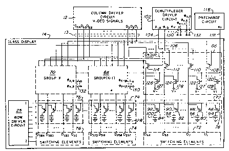
FTG. 2 is .a more detailed diagram of the substrate 14.
Again, a column control circuit 12, external to the
substrate, provides video signals on lines 13 to the
WO 94/10676 PCT/GB93J02195
... g
substrate 14. Also, the row driver circuit 25, which is
well known in the art and includes TFT transistors operated
from the control signals on line 21 in FIG. 1 from the
control circuit 12, sequentially selects a row as is well
known in the art. Rows are indicated in FIG. 2 as 1-Z rows
and only the first and last rows are shown. The remaining
rows are identical. It will also be noted in FIG. 2 that
there are X groups of Y switching elements. A switching
element comprises a transistor and its associated pixel
capacitor. In the first group designated by the numeral
72, there are shown only four switching elements 86, 88, 90
and 92 for purposes of simplicity. In actuality there
would be 64 such switching elements if the X groups were
six groups and the total number of columns used was 384
columns. The gates of the transistors 78, 80, 82 and 84,
which may be thin-film transistors deposited on the glass
substrate 14, are coupled through raw conductor 1 to the
row driver circuit 25. A pixel capacitor or display
element (94, 96, 98 and 100) is connected to the respective
source electrodes of the transistors 78, 80, 82 and 84.
The electrode 28 is the second plate of the pixel capacitor
and is the common electrode segment that is located on the
opposing substrate of the display 14.
A precharge circuit 116 generates an output signal on
line 118 that is coupled to the gates of all 384 precharge
transistors, one of which is coupled to each of the 384
column lines on the substrate .14. A sample of the
precharge transistors is shown in group 1, designated by
the block numbered 66. Precharge transistor 120 has its
drain connected' to a 'voltage source, V+; and its source
electrode coupled to internal data line column D~. All of
the odd column lines have such a transistor coupled
thereto. For instance, in FTG. 2, transistors 120 and 124 >~
have their drain electrodes coupled to a V+ voltage source
128. The transistors 122 and 126 for the even column lines
J
have their drain electrodes connected to a V- voltage
source 127. The 64 output lines D~_~ from the column
dV~ 94/ 1067b ~ ~ ~ ~ '~ ~ ~;. PCT/GB93/02195
t!f'.~.1
1~
driver circuit 12, indicated by the numeral 13, contain the
video signals that are coupled in parallel to each of the
X groups. For the present example wherein the number of
columns is set forth to be 384, there would be six groups
(X=6) of 64 columns~(Y=64) that receive the multipl.exal
video input signals from the input lines 13 in a
demultiplexed fashion. Demultiplexer circuit 102 generates
phase one and phase two pulses that are coupled to the
gates of demultiplexing transistors 108, 110 --- 112 and
114 in group one in block 66. Like signals on line pair
130 and line pair 132 from demultiplexer 102 drive groups
five and six (X-1 and X) designated by the numerals 68 and
_ 70. Thus demultiplexer driving circuit 102 firsts couples
the 64 video data input lines 13 to the 64 columns in the
ffirst group 72 of switching elements 86 88 --- 90 and 92,
then sequentially couples the 64 lines to each of the
successive groups 2 through X. Thus, the 64 data input
lines 13 are sequentially coupled to the next five groups
of switching elements including groups 74 and 76 as shown.
Each of the rows 1 through Z are also sequentially selected
where, in the example given, Z would be equal~to 240 rows.
One row is selected each time the 64 ingut data lines are
sequentially coupled to all of the six groups 1 - X.
Thus, in summary, FIG. 2 illustrates the block diagram
arrangement of the integrated data driver circuit. It has
a display which, for example only, provides a 384 X 240
pixel color hand-held TV. The horizontal pixel count is
384. The demultiplexer and precharge circuits 66 through
130 and 132, six groups, are fabricated with the thin-film
transistors on'the display itself to transfer video data
from the input lines 13 and to interface the display
directly to video signals on lines 13 from a video source.
As shown in FIG. 2, the video signals from the video source
(off -glass integrated circuits) are arranged to come onto
the display 14 sixty-four data lines at a time through
input data leads 13 (D~_~) using one-sixth of a designated
line time interval. The two control signals from the
PGT/GB93/02195
13'0 94!10676 r'
11
demultiplexing circuit 102 such as on lines 104 and 106
enable the first block of demultiplexing transistors 108,
110 -°-- 112 and 114 , in block 66 and transfer the video
signals on line 13 to switching elements coupled to the
display's first 64 internal data lines D~-Due. After
completion of the transfer of the data to the first 64
column switching elements, the next 64 video signals will
be transferred to the internal data lines D65°D~ZB during the
next one-sixth of the designated line time interval. This
is done by enabling a second pair of contra! signals for
the second demultiplexing circuit (not shown). The same
operation will continue sequentially for demulti- plexing
circuits in groups 3 through 6. The entire one row line of
video information is thus transferred to the internal data
lines in 42 microseconds of allocated data input time.
Seven additional microseconds are allowed for pixel
settling. Thus, the total data input time is 49
microseconds.
The advantage of this new demultiplexing driving
scheme is to reduce the number of external lead connections
from 384 to 79 and significantly solve the TFTLCDs'
assembly and packaging problems of the small connector
pitch. As a result, it reduces the manufacturing cost. In
addition to the demulti- plexing scheme using transistors
such as 108, 110 --- 112 and 114, a precharge transistor
such as transistors 120, 122 --- 124 and 126 are used to
simultaneously precharge their associated data line and
switching element to either a preselected voltage level V+
or V-, so that it requires discharge of the data lines to
' the preselected video signal level only during the data
signal input time interval. One such precharge transistor
is associated with each column line. With the invention as
shown, it utilizes only two transistors on each data line,
a demultiplexing transistor and a precharge transistor.
Therefore, the circuit is easy to manufacture with good
yield.
W094/10676 ~~~~~~ ~ PC.'1"/GB93/02195
-,
12
Referring now to FIG. 2 in conjunction with the timing
diagram in FIG. 3, it can be seen in line (a) of FIG. 3
that the scanning line time interval is approximately 63
microseconds for a 384 X 240 pixel display interfacing ,
with the NTSC TV system. The budgeted line time is 8
microseconds for previous line deselection, 6 microseconds
for scan data Line precharge, 42 microseconds for the video
data transferring in demultiplexed fashion from an external
video source to the X groups of data lines of the display
and 7 microseconds for the pixels to settle. This can be
seen in line (c). Thus, reviewing line (d) of FIG. 3, it
can be seen that during the f first 8 microseconds of the
_ deselect time, the previously scanned line, 1~_~, is
discharged from a select level such as 20 volts to a
negative 5 volts deselected level as shown in line (e) of
FIG. 3. This isolates all pixel capacitors in line n-1 so
that they hold their video data charge. Following the
deselect time of 8 microseconds, the precharge signal for
row n shown in line ( f ) rises to a preselected voltage such
as 25 volts for 6 microseconds. The transistors 120, 122
--- 124 and 126 are turned on such that the odd numbered
internal data lines D~, D3, -- D3~ are precharged to the V+
level and the even-numbered internal data lines Dz, D~, --
D3~ are precharged to V- level in 6 microseconds. The V+
voltage level is approximately 5 volts and the V- voltage
level is approximately 0 volts, for example. It should be
understood, however, that advantageously the V+ level may
be something less than 5 volts to increase the speed of
operation of the device. As can be seen in FIG. 5, during
the precharge time period of 6 microseconds, the internal
data line and the pixel capacitor may be charged to a V+
value that is less than the 5 volt maximum voltage. Then, ,
during the 7 microsecond time period for the data lines to
charge the pixel capacitors to the data input voltage
level, it requires the same time for QVZ to go from V+ to
the maximum data voltage and for 8V~ to be discharged to
the minimum data voltage. In both cases, the charge time
WO 94/10676 PGT/GB93/02195
~~~~~J~
e.:..::
13
for ~V2 and discharge time for 6V' can be shortened or
optimized. The data line and the pixel capacitor charge
time has been reduced to the amount of time required to
obtain OVZ and, if the required data line predetermined
voltage is less than 5 volts, the discharge time to the
required level is reduced by the amount of time equal to
discharge ~V2. In this manner, the V+ voltage level may be
optimized so that the time difference between charging an
internal data line and its associated pixel capacitor to
the maximum input vido data signal level, 5 volts for
example only, and discharging an internal data line and its
associated pixel capacitor to the minimum input video data
signal level, 0 volts for. example, is minimal. Thus, less
precharge time is required because the pixel capacitors are
not charged to the full value of 5 volts during the
precharge time period. The same analysis applies to the v-
voltage level 127 as to the even precharge transistors 122
126. After all internal data lines and the pixel
capacitors in a selected row such as 94 , 96 , --- 98 and 100
are precharged to either V+ or V- levels, the incoming
video data signals (red, green and blue) and their
complementary signals are sent to the data input lines
D1-D64. In this case, D~, D3, -- D63 are positive polarity
video signals and DZ, D4, -- D~ are their complementary
polarity video signals. These video signal voltages are
shown in lines (j) and (k) in FIG. 3. The control signals
from demultiplexer driver circuit~102 on lines 104 and 106
are raised to 25 volts and 30 volts, respectively, as
illustrated in dine (g) in FIG. 3 for 7 microseconds. Each
of the~other X groups of input lines, in this case X = 6,
have the video data on lines 13 coupled thereto for 7
microseconds as shown in lines (g), (h) and (i) in FIG. 3.
The'reason to divide the data lines into two groups, even
and odd, is because the data voltage polarity inversion
scheme is used in this system. The data voltage polarity
is altered between two fields of a TV frame. The last 7
~.~~3~~
W~ 94/10b76 ~ PCT/GB93/02195
j
14
microseconds of the 63 microsecond time interval is used to
allow the pixels in the last group, group X, to settle.
The demultiplexing transistors 108, 110 --- 112 and
114 are sized such that the internal data lines D~-D~ can
be discharged to within 15 millivolts of the incoming video
data color signal levels within the allocated time interval
of 7 microseconds in this example. A successive operation
is repeated for each of the demultiplexer circuits numbered
66~through 68 and 70, or all six groups.
At the beginning of the nth row line scanning
operation, the pixel switching transistors in row n are
already fully turned ON. Therefore, after the scanned row
n-1 is deselected, the pixels in row n are then precharged.
If the remaining 49 microsecond data input transfer time is
allocated in essentially equal time periods of 8
microseconds each, the first block of the pixel transistors
on columns D~-D~ in row n has the entire 49 microseconds
for pixel discharge times, the second block of the gixel
transistors in row n connected to columns D6~-D~Za has
approximately 41 microseconds discharging time. The third
block would have approximately, 33 microseconds and so
forth. The final block of the pixel transistors in row n
would have substantially only 9 microseconds left for pixel
discharging. By allocating 7 microseconds of time to each
of the six groups of pixel transistors and allowing the
final 7 microseconds for pixel settling as indicated in
FIG. 3(d), sufficient time is allowed for all of the pixel
transistors: to discharge. Short discharging time might
produce an error voltage 03DO1V for the sixth block of the
pixels. In order 'to reduce the 03DO1V and have a
resolution of 256 grey levels, it is desirable to allocate
the additional 7 microseconds for pixel settling time. In
this case, 14 microseconds will be available for the sixth
group of pixel capacitors to settle to their video signal
level. As line n-1 is being deselected as indicated in
line (e), line n is being selected and the voltage applied
WO 94/10676 ~ ~ ~ ~ ~ ~, PGT/GB93/02195
to that' line is at the maximum of 20 volts as indicated
(1) .
It is to be understood that the demultiplex ratio
affects the number of video leads and the number of signal
5 input leads. It can be optimized or compromised according
to the product application. For example, for high
resolution and/or high picture quality, one can use a
smaller demultiplex ratio so that more video signal leads
per group could be coupled into the substrate 14 instead of
10 64. One can also reduce a large number of input lead
counts for less demanding grade levels or sloraer speed
video products.
Further, in the present application, the data lines
and pixels are precharged to the highest needed voltage
15 levels due to the fact that N-channel transistors are used
for signal transferring and the data lines or pixels are
discharged while inputting video signals because it is much
easier and faster to discharge them than to charge them in
order to obtain an accurate signal voltage.
Further, ~1~ and ~~a (lines 104 and 106) can be
combined into one control line signal feeding all the gates
of multiplexing transistars 108 110 --- 112 and 114 in
group 1. The combining of signals ~t,e and ~~~o can be
accomplished when the gate voltage stress is not a concern
and the device characteristics of the demultiplexing
transistors 108, 110 --- 112 and 114 are goad enough to
discharge the internal data lines and pixel capacitors
uniformly. In like manner, the other demultiplexing line
pairs such as 130 and 132 to the other five groups,
including 68 arid 70 in FIG. 2, can be combined into one
control line for each pair. In such case, the number of
multiplexes gate control lines can be reduced to one-half
the number.
Thus the present invention discloses an active matrix
liquid crystal display in which the number of required data
input leads are reduced and the column and row driver
circuitry is integrated directly onto the display
PCT/GB93/02195
i
WO 94/10676
~~r
(::: '
16
substrate. This reduces costs and increases reliability
by eliminating the need for mounting integrated circuits on
a separate substrate.
For the example given herein, a 384 X 240 pixel color
hand-held TV is used. The horizontal pixel count is 384.
The demultiplexer and precharge circuits are fabricated
with thin-film transistors on the display itself to
transfer video data and to interface the display directly
to a video saurce. The video signals from a video source
external to the display are arranged to come onto the
display's 64 data lines at a time using one-sixth of a
designated line time interval. Twelve control signals, two
to each of the six groups, enable demultiplexing
transistors in six different blocks to sequentially
transfer the incoming video signals to the display's six
groups of 64 internal data lines. After completion of the
video data transfer to the first 64 internal data lines,
D~-Due, the next 64 video signals will be transferred to the
internal data lines D6$ thraugh D~Za. This is done by
enabling the second set of control signals of the
demultiplexing circuit. Each video data signal transfer
takes place during one-sixth of~ the designated line time
interval. This operation continues sequentially for all
six demultiplexing circuits. The entire one row of video
information is transferred to the internal data lines in 42
microseconds of allocated data input time.