Note: Descriptions are shown in the official language in which they were submitted.
- ' ~ 214836~
SPECIFICATION
'':.'~''
CODE DIVISION M~JLTIPLE ACCESS TRANSMITTER AND RECEIVER
TECHNICAL FIELD ~
The present invention relates to a transmitter and;
a receiver used in mobile communications based on a
code division multiple access (CDMA) system.
'
BACKGROUND ART
The following three systems are typical access
systems in mobile communications~
(1) SCPC/FDMA (Single Channel Per ~ ;
Carrier/Frequency Division Multiple Access) system.
(2) TDMA/FDMA (Time Division Multiple ~ ~-
Access/Frequency Division Multiple Access) system.
(3) CDMA system.
In the SCPC/FDMA system, a user occupies a channel
associated with a carrier. In TDMA/FDMA system, a
carrier is time-divided and each time slot is assigned
to a user. In these systems, a base station
communicates with a mobile station through an assigned ~
25 frequency, or an assigned frequency and time slot. ;
On the other hand, in the CDMA system, the output
:''' :'.
,; - ~ .' ~
- 2148356
.,
signal of primary modulation such as QPSK is converted
into a wideband signal by secondary modulation using a
spreading code, and is transmitted. Since many users
share the same carrier, and individual users are
identified by spreadlng codes, this system is referred
to as a spread spectrum multiple access system. The
CDMA system is further classified into a direct
sequence (DS) system and a frequency hopping (FH)
system. The direct sequence system is characterized
in that the primary modulated output signal is spread
by using a high rate spreading code. On the other
hand, the frequency hopping system resolves one symbol
into elements called chips, and translates the
individual chips into signals of different center
frequencies at a high rate. Since the FH system is
difficult to implement in the state of the art, the DS
system is usually used.
At a spread spectrum RF receiving end, a received
signal is demodulated in the order opposite to that at
the transmitting end. Specifically, secondary
demodulation which converts the wide-band received
signal into a narrow-band signal by despeading using a
spreading code is followed by primary demodulation
which recovers source information symbols by
~5 synchronous detection or delay detection. The
despreading at the receiving end is carried out by
-:-' 2~4~366
detecting correlation between the received signal and -
the spreading code corresponding to the desired signal
wave. Thus, the signal that has been spread by the
spreading code is despreadc
In the DS system, each bit (symbol) of binary
information is represented by a code sequence
consisting of so-called chips with an interval much
shorter than the interval of the bit, and the number
of chips per symbol is called a processing gain. This
is because the bandwidth of the transmitted signal is
expanded by a factor of the processing gain. Denoting
the processing gain as PG, 2PG PN (Pseudo-Noise) code
- sequences are generated, and they are the candidates
of the spreading codes. However, not all the PN codes
can be used as the spreading code because of some
correlations between them: Only a limited number of
the PN codes having small correlations can be used as ~;
the spreading codes. As a result, the actual capacity
in terms of the number of users per carrier is reduced ~'
to a fraction of the processing gain. Thus, a
plurality of carriers must be used in a CDMA cell of a
large capacity in terms of the number of subscribers.
In~other words, both the spreading code and the
carrier frequency must be designated to transmit and
receive a desired signal.
Fig. l is a block diagram showing a conventional
- 3 - ~ -
-' 21483~
transmitter, in which both a spreading code and a
carrier must be designated. In this figure, a
transmitted information signal applied to an input
terminal 11 is BPSK, QPSK, or GMSK (Gaussian filtered
Minimum Shift Keying) modulated by a primary modulator
12, and then supplied to a secondary modulator 13 as
an I-channel signal and a Q-channel signal (in the
BPSK, the in-phase signal I and the quadrature signal
Q are the same). On the other hand, a spreading code
generator 1~ generates the spreading code associated
with a desired received signal, and supplies it to the
secondary modulator 13. The spreading code generator
14 has a memory circuit for storing spreading codes,
and a function for selectively reading them. The
secondary modulator 13 multiplies the spreading code
with the I-channel signal and the Q-channel signal in
the form of a complex number, thereby carrying out the
secondary modulation.
The I-channel data and Q-channel data with the
bandwidth expanded by the secondary modulation are
converted into analog signals by D/A converters 15 and
16, respectively. The I-channel analog signal and the
Q-channel analog signal outputted from the D/A
converters 15 and 16 are supplied to a quadrature
modulator 17 that quadrature-modulates an IF
(intermediate frequency) carrier. The quadrature-
2 1483~ ~
modulated output is supplied to a frequency converter19 through a bandpass filter 18. The frequency
converter 19 converts an RF (radio frequency) signal
fed from a frequency synthesizer 21 to an RF modulated
signal by multiplying the RF signal with the
quadrature-modulated IF signal, and supplies the
modulated signal to a bandpass filer 22. The bandpass
filter 22 limits the passband of the modulated signal,
and supplies it to a power amplifier 23. The power :.
amplifier 23 power-amplifies the RF modulated signal,
and transmits it through an antenna.
Fig. 2 is a block diagram showing a conventional
receiver corresponding to the transmitter. A received
signal applied to an input terminal 31 is supplied to
15 a frequency converter 33 through a bandpass filter 32. ~:
The frequency converter 33 frequency-converts the :-
received signal into an IF signal using the local ~;
signal from a frequency synthesizer 34. The IF signal ~
is supplied to a quadrature detector 37 after its ~-
bandwidth is limited by a bandpass filter 35 and its
level is made nearly constant by an AGC circuit 36.
The quadrature detector 37 quadrature-detects the IF
signal, and outputs a baseband I-channel signal and a
baseband Q-channel signal. The I-channel signal and
Q-channel signal are converted into digital signals by
A/D converters 38 and 39, and then supplied to a
- 21~83~5)
correlation detector 41.
The correlation detector 41 despreads the digital
signals into narrow band signals, and supplies them to
a demodulator 42. The demodulator 42 primary-
demodulates the narrow band signals using synchronousdetection or delay detection, thereby recovering the
source transmission information. Although passive
devices such as a surface acoustic wave convolver
might be employed as the correlation detector 91,
matched filters or a sliding correlator,is practically
employed considering downsizing, or code multiple.
They carry out the digital signal processing in the
baseband region.
The foregoing conventional transmitter generates a
designated spreading code with the spreading code
generator 14, and the receiver despreads the spread
spectrum signal with the correlation detector 41 by
using the designated spreading code. In addition, the
frequency of the output signal is selected by the
frequency synthesizers 21 and 34.
Thus, in the conventional CDMA transmitter and
receiver, both the spreading code and the carrier
frequency must be designated simultaneously. In this
case, designation of a spreading code can be achieved
in a time sharing fashion by storing the spreading
codes in a memory because it is performed by a digital
;.,. . , . ~ ,. . ;: . .: : , . . . . :
-~21 48360
signal processing circuit in a baseband. Since
memories are maintenance free and appropriate for
downsizing, they are preferably applied to RF systems
that demand these features. On the other hand, since
5 the designation of the carrier is performed by the ~ -
frequency synthesizer in the RF band, it is difficult
to realize maintenance free and downsizing. For
example, although the processing gain of 256 requires
only a few carriers at most considering the capacity
10 in terms of the number of subscribers per cell, a ;
synthesizer for switching the carriers, or the same ;
number of local oscillators as the number of carriers
must be provided, and this will prevent downsizing.
DISCLOSURE OF THE INVENTION
Therefore, an object of the present invention is
to provide a CDMA transmitter and receiver that can ~
implement a downsized and maintenance free device.~;
Another object of the present invention is to
provide a CDMA transmitter and receiver that can
designate both the spreading code and carrier by a
digital signal in a baseband region.
In a first aspect of the present invention, there
25 is provided a code division multiple access -
transmitter comprising:
2 1 4 8 3 6 ~
a primary modulator for carryiny out primary
modulation of transmission information, thereby
generating a primary modulated I (In-phase) signal and
a primary modulated Q (Quadrature) signal;
spreading code generating means for generating a
spreading code which corresponds to a channel, and has
a frequency higher than a rate of the transmission
information;
a secondary modulator for performing spread
modulation of the primary modulated I signal and the
primary modulated Q signal using the spreading code,
thereby outputting spread I-channel data and spread Q-
channel data;
a frequency offset circuit for offsetting a center
frequency of the spread I-channel data and of the
spread Q channel data by a designated offset
frequency, thereby outputting frequency offset data;
and r
a transmitting circuit for converting the
~ 20 frequency offset data into a transmitted signal.
The frequency offset circuit may comprise: ::
a first signal generator for generating a cosine
wave of a frequency corresponding to the designated
offset frequency;
a second signal generator for generating a sine :
wave of the frequency corresponding to the designated
- 8 -
~- 2148366 : ~
offset frequency;
a first multiplier for multiplying the spread I- :
channel data by the cosine wave;
a second multiplier for multiplying the spread Q-
5 channel data by the sine wave; and ;
a first adder for summing an output of the first
multiplier and an output of the second multiplier.
The transmitting circuit may comprise a D/A :
converter for converting the frequency offset data
into an analog signal, and a frequency converter for
converting the analog signal into the transmitted
signal.
The frequency offset circuit may comprise: :
a first signal generator for generating a cosine ~
15 wave of a frequency corresponding to the designated ~ :
offset frequency;
a second signal generator for generating a sine
wave of the frequency corresponding to the designated i:
offset frequency; ::
a first multiplier for multiplying the spread I-
channel data by the cosine wave;
a second multiplier for multiplying the spread Q-
channel data by the sine wave; '
a third multiplier for multiplying the spread I-
25 channel data by the sine wave; -
a fourth multiplier for multiplying the spread Q-
,
." ".,-~ " ",: ,, ;. .: . .", ., ' - . ~ : " " " " " ~
' 2148360
channel signal by the cosine wave;
a first adder for adding an output of the first
multiplier and an output of the second multiplier; and
a second adder for adding an output of the third
multiplier and an output of the fourth multiplier,
thereby carrying out a complex multiplication of
the spread I-channel data and the Q-channel data with
the cosine wave and the sine wave, and outputting
frequency offset I-channel data and frequency offset
Q-channel data.
The frequency offset circuit may comprise:
a first memory circuit for storing a product of ~-
the spread I-channel data and a cosine wave of a
frequency corresponding to the designated offset
frequency;
a second memory circuit for storing a product of
the spread Q-channel data and a sine wave of the
frequency corresponding to the designated offset
frequency; ~ -
a third memory circuit for storing a product of
- the spread I-channel data and the sine wave;
a fourth memory circuit for storing a product of
the spread Q-channel data and the cosine wave;
a first adder for adding data read from the first
memory circuit and data read from the second memory
circuit; and
~, ', ' ~',; .,'"
, ~ 21~18 3 6 ~
a second adder for adding data read from the third
memory circuit and data read from the fourth memory
clrcult;
thereby carrying out a complex multiplication of
the spread I-channel data and the Q-channel data with
the cosine wave and the sine wave, and outputting
lrequency offset I-channel data and frequency offset ~ .
Q-channel data. : :
The frequency offset circuit may comprise:
a first memory circuit for storing a sum of a
product of the spread I-channel data and a cosine wave
of a frequency corresponding to the designated offset
frequency, and a product of the spread Q-channel data
and a sine wave of the frequency corresponding to the
designated offset frequency; and
a second memory circuit for storing a sum of a . ;
product of the spread I-channel data and the sine : .
wave, and a product of the spread Q-channel data and
the cosine wave,
thereby carrying out a complex multiplication of
the spread I-channel data and the Q-channel data with
the cosine wave and the sine wave, and outputting :
frequency offset I-channel data and frequency offset
Q-channel data.
The transmitter circuit may comprise D/A :~
converters for converting the frequency offset I-
214836u
channel data and the frequency offset Q-channel data
into analog signals, a quadrature modulator for
quadrature-modulating a carrier by an analog I-channel
signal and an analog Q-channel signal outputted from
the D/A converters, and a frequency converter for
converting an output signal of the quadrature
modulator into the transmitted signal.
In a second aspect of the present invention, there
is provided a code division multiple access receiver
comprising:
a first frequency converter for frequency-
converting a received slgnal into an IF (Intermediate
Frequency) signal;
a quadrature detector for converting the IF signal
into an I-channel baseband signal and a Q-channel
baseband signali ~;:
A/D converters for converting the I-channel : ;:
baseband signal and the Q-channel baseband signal into
~ digital signals; ;~
a second frequency converter for converting an I-
channel digital signal and a Q-channel digital signal
outputted from the A/D converters into signals with a
zero center frequency using a local signal of a : ~-
designated offset frequency, a center frequency of the
I-channel digital signal and of the Q-channel digital
signal outputted from the A/D converters being offseti
- 12 -
~ 2148360
a correlation detector for correlation-detecting
output signals of the second frequency converter; and
a demodulator for demodulating output signals of
the correlation detector.
The second frequency converter may comprise:
a first signal generator for generating a cosine
wave of the designated offset frequency;
a second signal generator for generating a sine
wave of the designated offset frequencyi
a first multiplier for multiplying the cosine wave
with the I-channel baseband signal converted into the
digital signal; and
a second multiplier for multiplying the sine wave
with the Q-channel baseband signal converted into the
digital signal.
The second frequency converter may comprise
lowpass filters for low-passing outputs of the first
multiplier and the second multiplier.
The second frequency converter may comprise an
automatic frequency control circuit connected to
outputs of the first multiplier and the second
multiplier.
The second frequency converter may comprise:
a low-suppress filter for suppressing low-
frequency components of outputs of the quadrature
detector;
, . . ., , , .. . . . .. , , .. . . ~ .. . - . . , . . - . ,
--" 21~836~
samp]ing means for sampling outputs of the low-
suppress filter at a clock frequency corresponding to
a designated offset frequency; and
a lowpass filter that low-passes outputs of the
sampling means.
In a third aspect of the present invention, there :~
is provided a code division multiple access system
including a code division multiple access transmitter
and a code division multiple access receiver, :
the code division multiple access transmitter
comprising:
a primary modulator for carrying out primary
modulation of transmission information, thereby
generating a primary modulated I (In-phase) signal and ~ :::;.
15 a primary modulated Q (Quadrature) signal; :~
spreading code generating means for : -
generating a spreading code which corresponds to a
channel, and has a frequency higher than a rate of the
transmission information;
a secondary modulator for performing spread
modulation of the primary modulated I signal and the
primary modulated Q signal using the spreading code,
thereby outputting spread I-channel data and spread Q~
channel data;
a frequency offset circuit for offsetting a
center frequency of the spread I-channel data and of ~: -
- 14 - ' -~ .
'' ~ :' ~' : "'
'~' ,'~' "' -
~' 21~836~
the spread Q channel data by a designated offset
frequency, thereby outputting frequency offset data; :
and -
a transmitting circuit for converting the
frequency offset data into a transmitted signal,
the code division multiple access receiver
comprising:
a first frequency converter for frequency-
converting a received signal into an IF (Intermediate
Frequency) signal;
a quadrature detector for converting the IF
signal into an I-channel baseband signal and a Q- ~:
channel baseband signal;
A/D converters for converting the I-channel
baseband signal and the Q-channel baseband signal into
digital signals; ':
a second frequency converter for converting
an I-channel digital signal and a Q-channel digital
signal outputted from the A/D converters into signals
with a zero center frequency using a local signal of a
designated offset frequency, a center frequency of the . ,
I-channel digital signal and of the Q-channel digital ~,
signal out,putted from the A/D converters being offset;
a correlation detector for correlation- :
detecting output signals of the second frequency
converter; and
- 15 - .
., . ., - , , , ~ . .. , . . , ,~ , -, ., ., -. , .. - ,, - , ~ .. ..
~ " , . ,.: ,, ", :, ~ ~ . " . . , , , , ,i , ,
.. . .. .. .. . .
' 21~836~
a demodulator for demodulating output signals
of the correlation detector.
According to the transmitter in accordance with
the present invention, designation of the carrier is
achieved by designating the offset frequency of the
frequency offset circuit. The receiver carries out
the designated frequency ccnversion of the baseband
signal in accordance with the offset frequency at the
transmitter. This makes it possible to achieve the
designation of bot~l carrier and spreading code in the
baseband using digital signals, thereby obviating a
frequency synthesizer or a plurality of fixed
frequency oscillators, and implementing downsized and
maintenance free CDMA transmitter and receiver.
~RIEF DESCRIPTION OF THE DRAWINGS
Fig. 1 is a block diagram showing a conventional
CDMA transmitter;
Fig. 2 is a block diagram showing a conventional
CDMA receiver;
Fig. 3 is a block diagram showing an embodiment of ~- -
a CDMA transmitter in accordance with the present
invention;
Fig. 4 is a block diagram showing an example of a ~'
frequency offset circuit 45 in Fig. 3; ~ -
- 16 ~
~ 21~836~
Fig. 5 is a block diagram showing a major portion
of another embodiment of a CDMA transmitter in
accordance with the present invention;
Fig. 6 is a block diagram showing an embodiment of
a CDMA receiver in accordance with the present
invention;
Fig. 7 is a block diagram showing an example of a
frequency converter 65 in Fig. 6;
Fig. 8 is a block diagram showing another example
of the frequency converter 65 in Fig. 6; and
Fig. 9 is a diagram showing frequency
characteristics illustrating the operation of the
frequency converter 65 when it is composed of a
frequency converting filter.
BEST MODE FOR CARRYING OUT THE INVENTION
EMBODIMENT 1
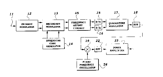
Fig. 3 is a block diagram showing an embodiment of
a transmitter in accordance with the present
invention. The transmitter differs from the
conventional transmitter shown in Fig. 1 in the
following:
(1) A frequency offset circuit 45 is inserted
between the secondary modulator 13 and the D/A
converters 15 and 16.
- 17 -
'"' . ' ,' ', ~. ~ ' ' ., " ' ".' '' , ' ~ ' ' ""
--' 21~1836~
(2) A fixed frequency osclllator 56 is connected
to the frequency converter 19 instead of the frequency
synthesi~er 21.
(3) The bandwidth of the bandpass filters 18 and
22 is set at least the conventional bandwidth
multiplied by the number of carriers.
The frequency offset circuit 45 shifts the center
frequency of the spread I-channel data and spread Q-
channel data outputted from the secondary modulator 13
by a designated offset frequency. An example of the
frequency offset circuit is shown in Fig. 4.
In Fig. 4, the spread I-channel data eos~n and the
spread Q-channel data sin~n are supplied to
multipliers 50 and 52, and 51 and 53, through input
terminals 48I and 48Q of the frequency offset eircuit
45, respectively. These channel data undergo a
complPx multiplication, in the multipliers 50 - 53,
with in-phase and quadrature offset frequency signals
outputted from signal generators 46 and 47.
More specifically, the signal generator 46
generates a cosine signal cos(+2~fi-t) of a
designated offset frequency ~fi, and supplies it to
the multipliers 50 and 53. On the other hand, the
signal generator 47 generates a sine signal
sin(+2~fi-t) of the designated offset frequency ~fi,
and supplies it to the multipliers 51 and 52. As a
- 18 -
~ 21~8366
..~ ,, .
result, the multiplier 50 outputs Cos~ncos(+2~fi t),
and the multiplier 51 outputs sin~nsin(+2~afi t). The
outputs are summed by an adder 59 which outputs the
frequency shifted spread I channel data
Cos(~n+2~fi-t). Likewise, the multiplier 52 outputs
cos~nsin(+2~afi-t), and the multiplier 53 outputs
sin~ncos(+2~afi-t). The outputs are summed by an
adder 55 which outputs the frequency shifted spread Q
channel data sin(~n+2~afi-t). Thus, the spread
channel data which are frequency offset in the
baseband region are generated by the complex
multiplication of the spread I channel data and the
spread Q channel data with the in-phase and quadrature
offset frequency signals.
The complex multiplication correspond to a
multiplication of the I-channel data and Q-channel
data represented by one complex number with the offset
frequency signals represented by another complex
number. In this case, it should be noted that the
sign of the offset frequency afi can be inverted by
switching sin(2~fi-t) with sin(-2~afi t).
The signal generators 46 and 97 can be composed of
a ROM storing cosine waves and sine waves. Having
st~red cosine signals and sine signals of offset
frequencies afi corresponding to respective
designatable carriers, and reading a pair of a cosine
- 19 -
: . . , . . -
: , : , : -
: . - . : , : : ~ .
.: . . , ~ . ~ . . .
~ 214836~
signal and a sine signal corresponding to a designated
carrier makes it possible to reduce the size of the
system.
In addition, the function of the signal generators
46 an 97 and the multipliers 50 - 53 can be
incorporated into a ROM by prestoring the results of
the multiplications of the I-channel data and Q-
channel data with the offset frequencies, and by
reading corresponding waveforms. Such an arrangement
can be implemented because the number of the spread I-
channel data and spread Q-channel data are limited,
for example, to four X the number of spreading codes,
in the case of QPSK.
Furthermore, even the adders 54 and 55 can also be
incorporated into a ROM by prestoring the frequency
shifted in-phase and quadrature components
corresponding to the combinations of the spread I-
channel data and spread Q-channel data with the offset
frequencies.
The frequency offset I-channel and Q-channel data
outputted from the frequency offset circuit 45 are ~-;
converted into analog signals by the D/A converters 15
and 16 as in the conventional system, and are supplied
to the quadrature modulator 17 through lowpass
25 filters. -
The quadrature modulator 17 quadrature-modulates
- 20 - - ~
' '
.~ ,~.,,,:". :, " ,,: ", ",, ~ ", ~;; "",~,"~ ".",,~
~ 2~1~8360
an IF carrier cos2~fc-t by the analog signals. The
quadrature-modulated output cos{~n+2~(fC~fi)t} is
converted into a transmission frequency by the
frequency converter 19 using an RF signal fed from the
fixed frequency oscillator 56, and is transmitted as a
signal cos{~n+2~(fh+~fi)t}. In this case, the center
frequency of a carrier i is fh+~fi. In other words,
the frequency of the carrier i is offset from the
frequency of the RF signal by +~fi-
Thus, designating the offset frequency
corresponding to the carrier frequency to the
frequency offset circuit 45 makes it possible to
frequency-offset the baseband signal by that offset
frequency. As a result, the frequency of the
transmitted signal can be set at the designated
carrier frequency.
The system in Fig. 9 can set the offset frequency
both in positive and negative directions because it
performs a complex multiplication. For example, when
the channels 1 - 8 are each frequency-offset
successively by ~f, the frequency range of the
channels 1 - 8 is from -4~f to +4~f by setting the
zero frequency at the center between the channels 4
and 5. In contrast, since the offset frequency must
be set in either the positive or negative direction in
the case of a real number multiplication, the
- 21 -
~' 214836u
frequency range of the channels 1 - 8 becomes 0 - 8~f.
Since the clock frequency of the signal processing in
the baseband region is determined by the absolute
value of the frequency range, the clock frequency
associated with the complex number multiplication can
be reduce to 1/2 as compared with that associated with
the real number multiplication.
The designated carriers are selected such that no
sidebands overlap with each other. In other words,
the frequency interval of the designated carriers is
made greater than the expanded bandwidth by the code
spreading. In addition, the passbands of the bandpass
filters 18 and 22 are selected such that they can pass
the carriers and their sidebands. For example, when , ,
the number of the carriers are three, the passbands of
the bandpass filters 18 and 22 of the present
embodiment are set at least three times wider than
those of the conventional bandpass filters. -
EMBODIMENT 2
Although the spread I-channel data and spread Q-
channel data undergo a complex multiplication with the
frequency offset signals in the first embodiment, an -
embodlment ls not restricted to this. For example, -~
these data can be frequency offset by real number
multiplications in the baseband.
- 22 -
214836~
Fig. 5 is a block diagram showing a major portion
of a transmitter with such a function. Signal
generators 46 and 47 generate cos(2~fi-t) and
sin(2~fi-t), which are supplied to the multipliers 50
and 51, respectively. The multipliers 50 and 51
multiply these signals with the spread I-channel data
and the spread Q-channel data, respectively, and
supply the outputs to an adder 57. The adder 57 sums
up the supplied signals and outputs the frequency
offset signal. The output of the adder 57 is
converted into an analog signal by a D/A converter 58,
and the analog signal is supplied to a frequency
converter 59 through a lowpass filter. The frequency
converter 59 converts the analog signal into an IF ~ -
signal using a signal cos2~fc-t from an oscillator 61.
In the present embodiment, the offset frequencies
- cannot range from the positive to negative domains as
in the first embodiment.
EMBODIMENT 3
Fig. 6 is a block diagram showing an embodiment of
a receiver in accordance with the present invention.
The receiver of Fig. 6 differs from that of Fig. 2 in
the following:
(1) A fixed frequency oscillator 64 is provided
instead of the frequency synthesizer 34 connected to
- 23 -
~ 2~48363
the frequency converter 33. The frequency converter
33 converts the received signal into an IF signal by
using a local oscillation signal from the fixed
frequency oscillator 69.
(2) The bandwidths of the bandpass filters 32 and
35 are set as at least the conventional bandwidths
multiplied by the number of the carriers.
(3) A frequency converter 65 is inserted between
the A/D converters 38 and 39, and the correlation ;
detector 41.
The frequency converter 65 converts the frequency-
offset baseband signal into a signal whose center
frequency is zero. More specifically, the IF signal
outputted from the frequency converter 33 is converted .-
into baseband I-channel and Q channel signals by the
quadrature detector 37. In this specification, the
baseband signal refers to a signal including no
carrier signal component. Specifically, the signals
after primary modulation and after spreading are
called a baseband signal at the transmitter end, and
the signals after quadrature detection and before
despreading, and after despreading are called a
baseband signal at the receiver end. The A/D
converters 38 and 39 convert the signals into digital -~--
data, the center frequencies of which are offset by
amounts corresponding to the offset frequencies at the
- 29 -
21483~
transmitter end. The frequency converter 65 converts
the baseband signal into a signal with the center
frequency of zero, and the offset frequency can be
designated by a value corresponding to each carrier
signal. The I-channel baseband signal and the Q-
channel baseband signal with the center frequency of
zero outputted from the frequency converter 65 are
converted into a narrow band signal by the correlation
detector 41, followed by the demodulation by the
demodulator 42.
Fig. 7 is a block diagram showing an example of
the frequency converter 6S together with the
neighboring circuits. The I-channel baseband signal
and the Q-channel baseband signal outputted from the
quadrature detector 37 are passed through lowpass
filters 66 and 67, thereby producing signals
Cos(~n~2~fi-t) and sin(~n+2~fi-t). In other words,
signals with their frequencies offset by +2~fi-t are
obtained. These signals are converted into digital
data by the A/D converters 38 and 39, and are supplied
to multipliers 68 and 69, to which local signals with
a frequency corresponding to that of the designated ~-
carrier are supplied from signal generators 71 and 72.
That is, a cosine local signal cos(+2~fi-t) is
supplied from the signal generator 71 to the
multiplier 68, and a sine local signal sin(~2~fi-t)
- 25 -
.,. -.
214836~
is supplied from the signal generator 72 to the
multiplier 69. The signal generators 71 and 72 are
the same as the signal generators 46 and 47 in Fig. 4.
The I-channel data cos~n and the Q-channel data
sin~n with the zero center frequency outputted from
the multipliers 68 and 69 will include a frequency ;
error and a fixed phase error. This is because the
quadrature detector 37 carries out quasi-synchronous
quadrature detection. The frequency error and the
fixed phase error are supplied to a digital AFC
(Automatic Frequency Control) circuit 75 through
lowpass filters 73 and 74, and are absorbed by the AFC
circuit 75. The output of the AFC circuit 75 is fed
to the correlation detector 41 of Fig. 6 so that the
transmitted source information is recovered through
the same processings as in the conventional system.
The frequency converter 65 is not restricted to~ -~
the circuit as shown in Fig. 7. For example, a ~ :
frequency conversion filter may be used which is
proposed in The Journal of the Institute of
Electronics, Information and Communication Engineers
of Japan 94/5 Vol. J77-B-II No. 5 pp. 235-236.
Fig. & is a block diagram showing the arrangement
of a frequency converter 65A using such a frequency
25 conversion filter 80. The frequency conversion filter~-~
80 has three stages. The first stage, a filter 81, is
,. . .
- 26 -
.,''. ''" ,' ', ', .,.''.'' ". '' '' ' ,, ,' '' ' : ', " '', . " ' '
'~' 21~836~
a low-suppress filter that suppresses low frequency
band of the output of the quadrature detector 37,
thereby eliminating noise components in the low
frequency band. For example, as shown in (A) of Fig.
9, components lower than a signal group are
eliminated, the signal group consisting of carriers X1
- X6 and their accompanying sideband waves which are
spread by code spreading components. The second
stage, a filter 82, is a filter that samples the
received signal at a predetermined clock frequency.
For example, to receive the signal X3 in the signal
group X1 - X6 in (A) of Fig. 9, the filter 82 samples
the output of the low-suppress filter 81 at the center
frequency X3. This will convert the signal X3 to a
signal whose center frequency is zero as indicated by
a shadowed portion in (B) of Fig. 9. The third stage,
a filter 83, is a lowpass filter that passes only the ;~
component whose center frequency is zero. As a
result, only the signal X3 with the zero center ~ ;
frequency is extracted as shown in (C) of Fig. 9.
Thus, a desired signal is extracted by selecting a
sampling frequency in accordance with a designated
.,:
' carrier.
. ~, ... :-
~ ,....,~, ~, .
- 27 -
,: . :