Note: Descriptions are shown in the official language in which they were submitted.
21~026
.
~PTICAL ~IGHTING ~VI~E
Technical Field
The present invention rela~es ~o ophth~lmo~optic
en~ineering, more spe~ifically ~o a par~lla~-free high-
s precisio~ di~e~t-visio~ æighting devi~e ai.med at use in
~eo~esy, milita~y prac~ic~, con~truG~ion engineering,
~iation, and na~igation.
Backg~oUnd Art
One ~xior-ar~ sight for firearm~ i8 knOWll ~0
c~mpri e a~ obj~ctive lens, a ligh~ source, and a
~i~h~ing mark i~ the ~or~ ~f a ligh~ ~pot, ch~a~ter~ze~
in th~t the ~igh~ing mark ~herein ~ n~e up o~ tw~
t~nd~m-arr~ng~d tr~nsparent (e.g., glass) cylinder~
mov~ble~.~n mut~lly square direc~ions, ~d ~ self-~ct~Ilg
n~ercu~y in ~w~tch i~ cu~ .in the 2~e~ic circ~i~ of ~he
~i~h~ so~lr~e and adapt~d f or b~aking the slectric
Gi7-CU~. o~ ~h~ l~mp when ~he g~ln ba~l is i~ a ver~ic~l
positlo~ (c.f. Inven~x's C~ e No. 21~,073). Thls
op~ical de~ice, however, s~ffe~s f~om subs~an~lal
~0 ~i~adv~ta~es, ~hat i~ 't f~ils tO p~ovide ~n ~nl~rged
in~ge of the object ~n~ to e~ec~ binocular aiming
~hout ~est~-ic~ing ~he angle of visual fi.el~, as well as
i~volves the effec~ of p~rall~x ~nd can~ot pro~ide
noc~ivi~io~.
Dis~losure of the Inve~ion
The present inve~tion has i~s principal ob~ect ~o
provide an optiGal si~h~ing devi~e capa~e of
~oç~ivi6ion, p~-oduGing an enlarged ima~ of th~ ec~
with a ~equi~ed magnification ~atio, pro~uci~g no op~içal
chang~s when the oper~to~ a]ces a si~h~ of the o~ject
}~einy ob~3erve~, ~n~blin~ one to e~fect binocul~r ~imi~
wi~hout limitirlg ~he angle of vi~;ual field, ~ree frorr ~h~
~f~ect: ~f par~llax, ~eaturirlg preci~ accu~acy of
aimirlg at a ~rget, ~nd being oE;era~ive in the ~wili~ht
3S and any clilna~e condi~ion~.
~ he fore~oing ob~e~t i~ ac~ompli~hed d-lç to the ~ct
that an optical si~h~ g device, c~mprisirl~ a light:
.
21~0~2
~,
sour~ and a si~h~in~ k, aGcor~iny ~o the in~ren~ion,
il1corpora~e~ adclitionally ligh~ ht oasirl~ which has
a window, whe~eill a ~ st elec~roopt~ical ~1utte~ and a
f~rst ligl~t-~plil:ting cube a~e locat~3d, whlle lo~ate~ in
fron~ of s~id cube on the side o~ the lnt~rn~l surface
~hereo~ . fi~s~ positive ~ens ~nd a bean~ split~er
having two ~egr~e~ o~ freed~m~ lo~a~ed on one ~ide o~
~ai~ ~eam ~pli~ter i~ a ~econ~l light~splitting cube, ancl
on the o~her side, an op~ical m~gni~yillg system, ~omposed
eeond, third, and ~ou~th lens and ~ s~ond
~le~tx~oo~ a~ shut~ex; located on one side of th~ ~3e~ond
ligh~-spl~ ng ~ube is a li~ emi~ing g~phic ~li9pl~y,
l on ~he o~her si~e, ~n op~ele~t~onic tran~d~ e~ ~nd ~
f if ~h 1~3115, said op~oelec~ronic: tralls~u~el- being
~onnec~ed ~o a p~w~r ~upply uni~ ~a~ing i~s ~ir~ ou~pu~
coTlnecte~ to ~ power ~ource, axld i~s ~e~on~ OU~ o
one of th~ inpu~s of an electro~.lic p~ocessor wh~se se~ond
i;~lpUt is c~n~ec~d ~o the o~itp~l~ of a ~on~rol panel, two
ou~puts of ~he ~lectrc~nic p~oce~ r ~e ~or~ne~ted to ~he
~o two elec~oop~:ical ~hu~er~, whil~ ~he ~hir~l out~?u~
th~eof is connec~ecl to t~le ligh~-emitt~in5 gr~phic
~i.splay .
Used ~ the li~ht-emit~ g g~phic d;~.~play .is
li~h~-emi~ting nl~t.~ix displa~ avai.lable from ~h~ "RS"
~SC~l'n~;?aIl~, c2~alo~T No. 56~-301, p . S4~ .
U~ed ~s t~e contxol p~n~ a push-l~utto~ COl'l X4 L
;pa~ vail~ble ~ron~ the l'~.S" ~ompany, ~a~alo~ No. 33S~
4~, P 9~
~rief Des~rip~ion of ~he Drawings
~o ~n wha~ ~ollows ~he presen~ invention is i~lustr~ d
~y ~h~ ~ccomp~nyin~ ~r~wings, whereill:
~ G. 1 i~. a ~lock-diasxam o~ the he~ein~propc~ed
optical si~h~ing device;
Fig. ~ is a view o~ a field of si~ht wi~hout
3~ magnif ica~ic)n of~ the ima~e; and
Fig. 3 is a ~iew of a fiel~ of sight wikh
m~ni~ic~kion of the im~e.
~1500~
.
~e~ Me~hod of Car~yillg Out ~h~ I~ve~ ion
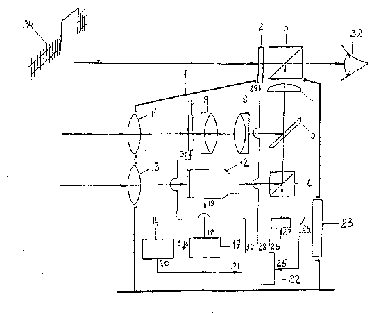
The op~ic~l ~ightlIl~ devi~e of the p~esent in~rentlo~
compri~es a ligh~:tigh~ ~sin~ having ~ window, w~erein a
first ele~ optic~l shutte~ 2 ~nd a first light-
spli~ing ~ube 3 ~ loca~ed c~n ~he outex side o sai~
wlndow . Locate~ ~ef ore the cube 3 on ~he inner side
t~ereo~ is a ~ir~ po~i~ive lex~ ~ and ~ be~m ~plit~ex 5
ha~ two deg~ee~ freedoTn, ~oca~ed on one side o~ the
m spli~tex 5 is a ~eco~d light-splitting cu~e ~, a
ht-emi~ing ~aphic di.~play 7 b~ing ~i~ua~ed on oIle
side ~ he ~u~e ~.
Loc~te~ on the other side o~ the ~eam s~ ter 5 is
a secon~ ~ens ~ an~ ~ thir-d lens ~ p~st ~hich ~ secorld
ele~t~oop~i~al ~hutter ~.0 is situate~, whi~h ~8 followed
~y a fourth lens 1~.
Situ~ed on ~he ~ther side of ~he li~ht-~pli~ing
cube ~ . is . an opt~ele~tronic tran~du~e~ whiçh i~
followe~ ~y a fi~th l~ns l~. A po~er sou~ce 1~ has i~s
output lS co2lnec~d to an input ~ of ~ power supply
unit 17 whi~h is c4nnected, through an ou~put 18, ~o an
inp~ 1~ of ~he optoele~r-o~ic ~r~nsdu~er 12. AI1 ou~put
20 of ~hP po~er source 14 is cv~nected to ~ input 21
of ~n electro~ic pro~es~or 22 ~ coJ.ltrol panel ~3, is
. co~lect~, thr~ugh i~s output 24, to an ill~U~ ~5 of ~h~
~5 p~ocesgor ~2. An outpu~ 26 of th~ processor ~ i.s
conne~ted to ~n i.nput 27 o~ the li~ht~emi~ing ~raphic
dlspla~ 7. An ou~put 28 ~ ~he process~ ~2 i~ c~nnecte~
to a~ i~put 2g o~ the elec~Aoo~tical ~hut~er 2~ A~
o~put 30 of the p~ocessor 2~ is connected to an input 31
of th~ electroop~ic~l shu~ter 10. An ~per~tor~s eye is
indic~d a~ Re.~o.32, a si~hting mal-ker, ~t Ref.~o.33,
an object bein~ aine~ a~ ~ein~ indicate~ with Ref.~o.34,
and a field of a~ enlarged im~ge of ~he o~ject 34, at
Ref.No.~S.
The op~ic~l sigh~in~ ~evice o~ the present inv~n~ion
operate~ as follow~.
The opelAator's eye 3~ looks ~ the dist~n~ o~j~ct 34
,
4
~h~ough ~he cube 3 an~ the e~e~trooptical shutte~ 2, th~
~eing the o~ject without magrlifi~a~ion.
Tne light r~ys emitted by ~e light-emi~tin~ gr~phi~
di..spl~y 7 ~re ~nsm.it~ed t~rough tlle light-splittin~
~ube ~, the beam-split~er ~, ~he ligh~-r~fle~ting s~r~ce
o~ the cu~e 3 ~Ild get iI~cide~t upon ~he oper~tor~s eye
3~. In ~}lis ~se ~he oper~tor's ~ye sees ~he image o~ ~he
o~j~c~ 34 an~ tha~ of the ~uminou~ marker ~3 superimposed
~he~eo~,
For a mo~e accur~e ~iming of ~he s~ght~Ilg ~evic~
th~ c~ 34 ~ei~g aimed at, ~e operato~ ~w1~he~ o~,
using the c~nt~o~ panel 23, ~h~ first elec~ooptica~
shu~t~ which c~-eates a darke~d spo~ its c~ntra7.
por~ion, ~he field 35 of a magnified image o~ the object
~4 ~ei~g pro3ected ~nto said dark~n~d ~pot.
T~e d~rke~ed ~pot an~ ~he fie~ 3$ 3f an enl~r~ed
im~e o~ th~ o~ec~ 3~ mea~ure ~llke. Simultan~ously ~he
elec~r~optic~l s~hutter 10 is swi~ched on to change it
o~r ~rom ~ no~ransparent to tran~pa~nt state.
The lenses 11, ~, and ~ ~re in f~c~ ~ ma~nifyi~
~ptlc~ a~n or ~stem fo~ the o~ie~t 34 who~e ima~,
while be~ g re~lected from one of ~he sllrf~s o~ th~
~eam spli~er 5 and havi~g pas~ed th~:ough t~ 5 4,
ge~s illcident upon the li~h~-refl~ç~ g surface cf the
25~ cube ~ establishi~y a~ enlar~ed i.mage ~f the o~3eçt
34 i~ the op~ato~'s ~ye 32, s~id ima~e ~ s~
a~ains~ ~ back~roun~ of ~he darkene~ spo~ ~ the
ele~rooptic~1 shutter 2. In this ~ase ~he oper~tor's eye
3~ sees an undi~o~te~ image o~ the object 34 o~f ~he
enlarged fiel~, ~nd an enlarsed image of the objeGt 34
and the luminous ~arke~ 33 in ~he field ~5 of ~n e~la~e~
image o~ th~ object 3~.
The lens 13 and the optoelec:tr~nic t~n~ducex 12
mak~ ~p a ni~ht-vision optical s~s~em which ~onver~ an
infr~xed ra~ia~lon of the ob~ec~ 3~ in~o the visi~le
sp~c~rum. Th~s, sa~d image g~t~ upon the oper~o~s ey~
32 after havll1g pas~ed th~ough ~he ~u~e ~, the beam
213 0~2 ~
5
sp].i~ter 5, t~e lens 4, and th~ c~e 3; a~ a result, ~he
oper~or r ~ e~e sees a~l in~ra~ed inlage of the o~ j~ct ~4 a~
co~verted in~o t~le visible spe~um, with t~h~ im~e o~
the luminou~ marl~er 3 3 s~perimposed ~hereon .
rh~ el~ctroni~ process~r 22 receiver command signals
from the cont~ol panel 23 so as ~o control ~he opera~ion
o~ the ~le~t~optiG~l ~hutte~s 10 and ~, and the ~i~ht-
emi~ting graphlc display 7.
Indus t~ia~ Appl icabil i~y
The p~esent inventlon can find ~ppli~ion in
geod~sy, mi~ itary practic~ t~uc~ion engineerin~,
aviatioxl, ~nd navi~ on.