Note: Descriptions are shown in the official language in which they were submitted.
PCT/GB94I00003
WO 94/16428 v
1
A DATA DRIVER CIRCUIT FOR USE WITH AN LCD DISPLAY
The present invention relates generally to video
displays and their associated driving circuits and in
particular to LCD video display column driving circuits
that use a simplified multiplexing arrangement for data
lines and pixel capacitors that are precharged to a
selected voltage level prior to the application of video
data signals to enable selected ones of the data lines and
pixel capacitors to be additionally charged or discharged
to an appropriate level by the incoming video data signals
to enhance the operation of the display.
Matrix display devices commonly utilize a plurality of
display elements that are arranged in a matrix of rows and
columns and supported on opposing sides of a thin layer
of
electro-optic material. Switching devices are associated
with the display elements to control the application of
data signals thereto. The display elements include a pixel
capacitor driven by a transistor as a switching device.
One of the pixel electrodes is on one side of the matrix
display and a common electrode for each of the pixels is
formed on the opposite of the matrix display. The
transistor is usually a thin-film transistor (TFT) that
is
deposited on a transparent substrate such as glass. The
switching transistor has its source electrode connected
to
the pixel electrode that is deposited on the glass on the
same side of the display matrix as the switching
transistor. The drain electrodes of all of the switching
transistors in a given column are connected to the same
column conductor to which data signals are applied. The
gate electrodes of all of the switching transistors in a
' given row are connected to a common row conductor to which
row selection signals are applied to switch all the
transistors in a selected row to the ON condition or state.
By scanning the row conductors with the row selection
signals, all of the switching transistors in a given row
are turned ON and all of the rows are selected in a
CA 02150454 2002-02-13
2
sequential fashion. At the same time, video data signals are
applied to the column conductors in synchronism with the
selection of each row. When the switching transistors in a
given row are selected by the row select signal, the video
data signals supplied to the switching transistor electrodes
cause the pixel capacitors to be charged to a value
corresponding to the data signal on the column conductor.
Thus each pixel with its electrodes on opposite sides of the
display acts as a capacitor. When the signal for a selected
row is removed, the charge in the pixel capacitor is stored
until the next repetition when that row is again selected
with a row select signal and new voltages are stored therein.
Thus a picture is formed on the matrix display by the charges
stored in the pixel capacitors.
It is also known to precharge the pixel capacitors of the
presently selected row to a predetermined voltage level prior
to the video data signals being applied to the column
conductors as set forth in commonly assigned US Patent
No. 5,426,447. By doing so, the pixel capacitor can then be
additionally, charged or discharged to the level of the
succeeding video data in a shorter time period than required
if the pixel capacitor was charged only the video data
signals. To accomplish the precharging function, precharging
TFTs are deposited onto the glass substrate with each of the
drain electrodes connected to a column conductor and each of
the gate electrodes connected together and to a precharge
circuit and each of the source electrodes connected to a
predetermined voltage source.
Then prior to the video data signals being applied, the
precharge circuit turns ON each of the precharging TFTs
thereby allowing the voltage source to charge the pixel
capacitors, to a predetermined level.
EP-A-0417578 discloses a liquid crystal .display with
multiplexing actuating circuit, WO 92/09986 discloses a logic
circuit for an amorphous silicon scanning matrix system.
zl~o~
3
It is to be understood that the use of the term
"video" herein, although it has been generally applied to
the use of signals for television, is intended to cover
displays other than TV pictures or displays. Such displays
may be hand-held games having an LCD display with moving
figures thereon and the like.
The present invention is directed to a new data driver
circuit for use with a scanned LCD video display.
According to the present invention, there is provided a
circuit for providing video data to a display having a
matrix array of pixel cells in rows and columns, and
wherein the display has first and second substrates, at
least the first of which is glass, separated by a layer of
electro-optic material, the circuit comprising:
Y input column lines deposited on one of the
substrates;
X groups of Y demultiplexer elements deposited on said
one of the substrates wherein each demultiplexing element
is direclty connected to one of the Y input column lines;
a demultiplexing circuit external to the first
substrate having X enabling signal means respectively
connected to the X groups of Y demultiplexing elements for
enabling each of the X groups of Y demultiplexing elements;
and
a control circuit external to the first substrate
having Y output lines connected to the Y input c~iumn lines
for coupling the video data and a precharging voltage to
the Y input column lines to charge each pixel cell in each
sequentially selected row to a predetermined DC level such
that the precharging voltage is provided prior to the video
data being coupled to the Y input column lines, and wherein
the demultiplexing circuit simultaneously enables each of
the X groups of Y demultiplexing elements when the
precharging voltage is provided, and consecutively enables
the X groups when the video data is provided.
In the present invention using a 384 X 240 pixel color
hand-held TV as an example, the demultiplexer elements are
AMENDED SHEET
i
2150454
4
fabricated as thin-film transistors (TFTs) on the display
itself to transfer a precharging voltage and video data
from an off-glass source to the on-glass pixel capacitors
of the display. The demultiplexer elements are divided
into a predetermined number of groups and a demultiplexing
circuit controls the activation of these groups. The
demultiplexing circuit consecutively and sequentially
enables each of the groups of demultiplexer elements in
order to provide video uata to charge the pixel capacitors
to a corresponding level. Prior to the video data being
provided, a control circuit provides a precharging voltage
and the demultiplexing circuit enables each of the groups
of demultiplexer elements simultaneously to allow all of
the pixel capacitors of the selected row to be charged to
a predetermined level.
Therefore, it is an object of the present invention to
provide a simplified means for precharging the pixel
capacitors.
It is a further object to reduce the manufacturing
costs of the LCD display by reducing the number thin-film
components required to be deposited on the display.
It is a still further object of the present invention
to provide a more reliable column data driver circuit by
reducing the number of on-glass components required.
These and other features of the present invention will
be more fully disclosed in the following detailed
description of the drawings in which like numerals
represent like elements and in whic.z: '
FIG. 1 is a basic block diagram of the novel system
and data driver circuit for a self-scanned TFTLCD video
display;
FIG. 2 is a detailed diagram of the matrix array on
glass and the data scanning circuits associated therewith
in accordance with the present invention;
FIG. 3 is a detailed diagram of a matrix array and
data scanning circuits disclosed in a commonly assigned
copending patent application;
AMENDED SHEET
CA 02150454 2002-04-10
4A
FIG. 4 illustrates the waveforms and timing of the
present invention;
FIG. 5 is a diagram of a capacitor charge waveform
illustrating that a capacitor discharges faster than it
charges; and
FIG. 6 is a waveform illustrating the time saving
benefits of applying less than a full precharge voltage V+
or V- to the pixel capacitors.
The circuit of FIG. 3 is disclosed in detail in
commonly assigned US Patent No. 5,426,447 .entitled "DATA
DRIVING CIRCUIT FOR LCD DISPLAY".
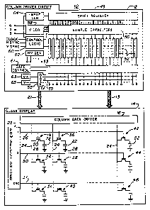
FIG. 1 is a basic block diagram of the novel display
system 10 which includes the display device 14 and the
"off-glass" control circuits 12 that are separate from and
connected to the display 14 to drive the elements thereon.
An active matrix liquid crystal display (AMLCD) of the type
illustrated in FIG. 1 may typically consist of 200,00 or
more display elements. Clearly, for displaying television
pictures, the greater the number of display elements, the
greater the resolution of the picture. For a hand-held TV,
for example, the array may include 384 columns and 240
rows. In such a case, in excess of 92,000 display elements
or pixels are required. For larger sets, of course, the
number increases. The transistors used to drive the pixels
are usually thin-film transistors TFTs) deposited on a
substrate such as glass. The display elements include
electrodes deposited on the glass and common electrode
elements on an opposing substrate, the opposing substrates
being separated by an electro-optic material. On. the
CA 02150454 2002-02-13
substrate 14, which may be glass, the column data driver
circuits 16 drive the column lines 24 with the video data
signals and~precharging voltage. The row select driver 25 may
be of any type well known in the art, preferably of the type
disclosed in commonly assigned US Patent No. 5, 313, 222 and
entitled ~~A SELECT DRIVER CIRCUIT FOR AN LCD DISPLAY", and
sequentially activates the pixels in each selected row and
the rows 1 through 240 are driven sequentially.
In the external control circuits 12 that are separate
from the display 14, sample capacitors 50 receive data from
input circuit 64 through shift register 49. The red, green
and blue video signals are coupled from circuit 58 to the
sample capacitors 50 in concert with the data in the shift
registers 49. The clock signals and horizontal and vertical
synchronization signals are provided by control logic 60. A
high voltage generator 62 provides the necessary high voltage
power. The output of the sample capacitors 50 are coupled to
64 output amplifiers 52. In turn, the amplifiers 52 are
coupled to a gate 53 for controlling the output of the video
data. A gate 55 is coupled to voltage sources 63 and 65 and
controls the voltages on lines 57 and 59 to allow a
precharging voltage to be provided to substrate 14. A gate
control 61 controls gates 53 and 55 such that only one gate
is enabled at a time. Line 57 is coupled to each odd output
line D1, D3 --- D63 and line 59 is coupled to each even input
line D2, DQ --- D6q.
Thus, if one row of pixels includes 384 display elements,
the 64 data input lines 13 are coupled in multiplexed
fashion, 64 bits at a time, to the 384 display elements on
the substrate 14 after a precharge voltage is applied. The 64
video outputs are coupled on line 13 to the column conductors
24 through column data drivers 16 as will be disclosed
hereafter.
As seen in FIG. 2, lines 104, 106, 130, and 132 from
a demultiplexing circuit 102 form six pairs of
WO 94116428 PCT/GB94100003
2150454
6
enabling signal lines that are applied to X(6) groups,
designated as 66, --- 68 and 70, of Y(64) demultiplexing
elements. These elements are designated as 108, 110 ---
112, and 114 and are deposited on glass 14 to demultiplex
the 64 output signals and couple them sequentially to the
X (6) different groups (66 -- 68, 70) of Y(64) column lines
24 in a selected one of Z (240) rows on the glass 14.
Also, the lines 104, 106, --- 130, and 132 enable all 384
demultiplexing elements (108, 110 --- 112, and 114 in each
l0 group) simultaneously for a time period prior to the video
data being applied to substrate 14 to allow the display
elements to be precharged to a predetermined voltage level.
The row select driver signals, the clock and power lines
are coupled from the control circuit 12 on line 21 to the
row select driver circuit 25 as shown in FIG. 1. Row
select driver circuit 25 may be any of such type of
circuits well known in the art but is preferably of the
type disclosed in commonly assigned copending application
Serial No. 996979 filed December 24 1992.
As shown in FIG. 3, if the first row is selected by
row select driver circuit 225, the transistors 278, 280,
282, and 284 in row 1 will all be activated. Then, a
precharging circuit 316 and the X column data driver
circuits 266, --- 268, and 270 will provide signals that
will precharge each column line and each of the pixel
capacitors 294, 296, --- 298, and 300 in the first row of
row driver 225 to a preselected voltage. Then, as the data
signals are applied to the column lines 224, the capacitors
will be further charged or discharged by an amount that
depends upon the level of the data signal being applied to
the column lines 224. Precharge of the capacitors is used
because the capacitors 294, 296, --- 298, and 300 are able
to discharge much faster than they charge as illustrated in
FIG . 5 . As can be seen in FIG . 5 , f or the capacitor to
charge from 0 to a value designated by the numeral 23,
takes X amount of time. However, f or the capacitor to
discharge from its maximum value to that same level takes
WO 94!16428 PCTIGB94J00003
,:. ~15Q45~
7
only Y amount of time which is much smaller than X.
Further, it takes time, t, to charge to its full amount and
a lesser time, Z, to discharge completely. Thus, the
discharge times are much more rapid than the charge times
thereby enabling the discharge of the data line capacitors
to their proper voltage level during the data signal input
time interval. This can shorten the time required for the
data input time interval.
Thus, in the circuit of FIG. 3, a precharge circuit
l0 316 generates an output signal on line 318 that is coupled
to the gates of all 384 precharge transistors 320, 322,
324, and 326, one of which is coupled to each of the 384
column lines on the substrate 214. A sample of the
precharge transistors is shown in group 1, designated by
the block numbered 266. Precharge transistor 320 has its
drain connected to a voltage source, V+, and its source
electrode coupled to internal data line column D~. All of
the odd column lines have such a transistor coupled
thereto. For instance, in FIG. 3, transistors 320 and 324
have their drain electrodes coupled to a V+ voltage source
328. The transistors 322 and 326 for the even column lines
have their drain electrodes connected to a V- voltage
source 327.
The present invention eliminates the need for the
precharging circuit 316 and transistors 320, 322 --- 324,
and 326 of FIG. 3 while still maintaining the precharging
function and advantages outlined above, as seen by
comparing FIG. 3 with FIG. 2. As shown in FIG. 1, this is
accomplished by alternatively turning OFF gate 53 and
turning ON gate 55 with gate control 61 to allow voltage
sources 63 and 65 to charge lines 57 and 59 to a
- predetermined level for a specif ied time period. Then, for
the same time gate 55 is turned ON, demultiplexing circuit
102 in FIG. 2 simultaneously enables the X groups of Y
demultiplexing elements (108, 110 --- 112, and 114) shown
in FIG. 2. This allows capacitors 94, 96, 98, and 100 to
be charged to the predetermined voltage.
WO 94/16428 _ PCTIGB94/00003
8
Thus, with each row sequentially energized, all of the
pixel capacitors in all groups in a selected row are
charged simultaneously to their predetermined value and are
discharged sequentially in X groups as the video signals
are received. Thus, X groups of Y switching transistors
(78, 80, 82, and 84) in Z rows are deposited on the
substrate 14. If the display should be, for example only,
a 384 X 240 pixel display, there could be six groups of 64
switching elements in 240 rows deposited on the substrate.
l0 Such example will be discussed herein.
FIG. 2 is a more detailed diagram of the substrate 14.
Again, a control circuit 12, external to the substrate,
provides precharging voltages and video signals on lines 13
to the substrate 14. Also, the row driver circuit 25,
which may be of the type previously described, includes TFT
transistors operated from control signals on line 21 in
FIG. 1, sequentially selects a row, as is well known in the
art. Rows are indicated in FIG. 2 as 1-Z rows and only the
first and last rows are shown. The remaining rows are
identical. It will also be noted in FIG. 2 that there are
X groups of Y switching elements. A switching element
comprises a transistor and its associated pixel capacitor.
In the first group designated by the numeral 72, there are
shown only f our switching elements 86, 88, 90, and 92 for
purposes of simplicity. In actuality there would be 64
such switching elements if the X groups were six groups and
the total number of columns used was 384 columns. The
gates of the transistors 78, 80, 82, and 84, which may be
thin-film transistors deposited on the glass substrate 14,
are coupled through row conductor 1 to the row driver
circuit 25. A pixel capacitor or display element (94, 96,
98, and 100) is connected to the respective source
electrodes of the transistors 78, 80, 82, and 84. The
electrode 28 is the second plate of the pixel capacitor and
is the ground or common electrode segment that is located
on the opposing substrate of the display 14.
WO 94116428 PCTIGB94100003
21~~4~4
9
In contrast to the circuit of FIG. 3, the present
invention, as seen in FIGS. 1 and 2 generates a precharging
. voltage in lines D~ through D~ when gate control 61 turns
OFF gate 53 and opens gate 55. Gate control 61 alternately
enables and disables gates 53 and 55 such that only one
gate is enabled at a time. This allows voltage sources 63
and 65 to charge the odd and even lines D~ through Due,
respectively. While gate 55 is open, demultiplexing
circuit 102 generates clock signals to turn ON transistors
108, 110 --- 112,~and 114 in all groups, thus allowing all
capacitors 94, 96, 98, and 100 to be charged in the
selected row.
As seen from the above discussion, the present
invention allows the elimination of 384 TFTs (320, 322,
324, and 326) on the display substrate shown in FIG. 3.
This, in turn, reduces manufacturing costs and increases
production yield and reliability. The function of
precharge circuit 316 is performed by control circuit 12
and demultiplexing circuit 102 in the present invention.
After the precharging function is perfonaed, the operation
of the circuit of FIG. 3 and the circuit of the present
invention are exactly the same.
Referring now to FIG. 2 in conjunction with the timing
diagram in FIG. 4, it can be seen in line (a) that the
scanning line time interval is approximately 63
microseconds for a 384 X 240 pixel display interfacing with
the NTSC TV system. The budgeted line time is 8
microseconds for previous line deselection, 6 microseconds
for scan data line precharge, 42 microseconds for the video
data transferring in demultiplexed fashion from an external
video source to the X groups of data lines of the display
- and 7 microseconds for the pixels to settle. This can be
seen in line (c). Thus, reviewing line (d) of FIG. 4, it
can be seen that during the f first 8 microseconds of the
deselect time, the previously scanned line, r.-1, is
discharged from a select level such as 20 volts to a
negative 5 volts deselected level as shown in line (e) of
WO 94/16428 , z y PCTIGB94I00003
FIG. 4. This isolates all pixel capacitors in line n-1 so
that they hold their video data charge. Following the
deselect time of 8 microseconds, the precharge signals for
row n shown in lines (i) and (j) adjust to a preselected
5 voltage such as 15 volts for 6 microseconds. As shown by
the first pulse in lines (g), (h), (i) and (j), during this
6 ~s precharge time all demultiplexer signals are pulsed
high. This turns ON transistors 108, 110 --- 112, and 114
in all groups such that odd numbered data lines, D~, D3 ---
10 D383, are charged ~to the V' level and even numbered data
lines, DZ, D~ --- D3~, are charged to the V level. In
contrast, in the circuit of FIG. 3, ~x from precharge
circuit 316 would be pulsed high to turn ON the transistors
320, 322 --- 324, and 326 such that the odd numbered
internal data lines D~, D3, -- D383 are precharged to the V+
level and the even-numbered internal data lines Dz, D4, --
D3~ are precharged to V level in 6 ~.s. So it can be seen
that the first precharge pulses of lines (f), (g), (h), (i)
and (j) of FIG. 4 replace the function of ~x of the circuit
in FIG. 3. It is also noted, as those skilled in the art
will appreciate, that in line (f) of FIG. 4 a single pulse
of approximately 13 ~s could be used to replace the two
consecutive precharge and video control pulses shown. This
is because the second pulse follows the first so closely
that a single pulse would have the same effect.
The Vf voltage level is approximately 5 volts and the
V voltage level is approximately 0 volts, for example. It
should be understood, however, that these voltage levels
may vary to increase the speed of operation of the device.
As can be seen in FIG. 6, during the precharge time period
of 6 ~s, the internal data line and the pixel capacitor may
be charged to a V+ value that is less than the 5 volt
maximum voltage. Then, during the 7 ~s time period for the
data lines to charge the pixel capacitors to the data input
3 5 voltage leve 1, it requires the same time f or ~Vz to go from
V+ to the maximum data voltage and for ~V~ to be discharged
to the minimum data voltage. In both cases, the charge
WO 94/16428 , . ~ ~ PCTlGB94100003
11
time for AVZ and discharge time for AVM can be shortened or
optimized. The data line and the pixel capacitor charge
time has been reduced to the amount of time required to
obtain ~VZ if further charging is required and, if the
required data line predetermined voltage is less than 5
volts, the discharge time to the required level is reduced
by the amount of time equal to discharge ~V~. In this
manner, the V' voltage level may be optimized so that the
time difference between charging an internal data line and
its associated pixel capacitor to the maximum input video
data signal level, 5 volts for example only, and
discharging an internal data line and its associated pixel
capacitor to the minimum input video data signal level, 0
volts for example, is minimal. Thus, less precharge time
is required because the pixel capacitors are not charged to
the full value of 5 volts during the precharge time period.
The same analysis applies to the V voltage level as to the
V? voltage level.
After all internal data lines and the pixel capacitors
in a selected row such as 94, 96, --- 98, and 100 are
precharged to either V' or V levels, the incoming video
data signals (red, green, and blue) and their complementary
signals are sent to the data input lines D1-D64. In this
case, D~, D3, -- D63 are positive polarity video signals and
Dz, D4, -- D~ are their complementary polarity video
signals. These video signal voltages are shown in lines
(i) and (j) in FIG. 4 as dashed lines following the
precharge time. The control signals from demultiplexer
driver circuit 102 on lines 104 and 106 are raised to 25
volts and 30 volts, respectively, as illustrated in line
(f) for 7 ACS. Each of the other X groups of input lines,
in this case X = 6, have the video data on lines 13 coupled
thereto for 7 ~,s as shown in lines (f) , (g) , and (h) in
FIG. 4. The reason to divide the data lines into two
groups, even and odd, is because the data voltage polarity
inversion scheme is used in this system. The data voltage
polarity is altered between two fields of a TV frame. The
WO 94/16428 PCT/GB94100003
~, 21~5P04~4
12
last 7 ~s of the 63 ~s time interval is used to allow the
pixels in the last group, group X, to settle better.
The demultiplexing transistors 108, 110 --- 112, and
114 are sized such that the internal data lines D~-D~ can
be discharged to within 15 millivolts of the incoming video
data color signal levels within the allocated time interval
of 7 acs in this example. A successive operation is
repeated for each of the demultiplexer circuits numbered 66
through 68, and 70, or all six groups.
At the beginning of the n~h row line scanning
operation, the pixel switching transistors in row n are
already fully turned ON. Therefore, after the scanned row
n-1 is deselected, the pixels in row n are then precharged.
If the remaining 49 /cs data input transfer time is
allocated in essentially equal time periods of 8
microseconds each, the first block of the pixel transistors
on columns Di-D~ in row n has the entire 49 microseconds
for pixel discharge times, the second block of the pixel
transistors in row n connected to columns D65-D~28 has
approximately 41 us discharging time. The third block
would have approximately 33 ~.s and so forth. The final
block of the pixel transistors in row n would have
substantially only 9 us left for pixel discharging.
By allocating 7 us of time to each of the six groups
of pixel transistors and allowing the final 7 us f or pixel
settling as indicated in FIG. 4(d), sufficient time is
allowed for all of the pixel transistors to discharge.
Short discharging time might produce an error voltage AV
for the sixth block of the pixels. In order to reduce the
AV and have a resolution of 256 grey levels, it is
desirable to allocate the additional 7 microseconds for
pixel settling time. In this case, 14 microseconds will be
available for the sixth group of pixel capacitors to settle
to their video signal level. As line n-1 is being
deselected as indicated in line (e), line n is being
selected and the voltage applied to that line is at the
maximum of 20 volts as indicated (1).
WO 94/16428 PCTIGB94/00003
~l~o~
13
It is to be understood that the demultiplex ratio
affects the number of video leads and the number of signal
input leads. It can be optimized or compromised according
to the product application. For example, for high
resolution and/or high picture quality, one can use a
smaller demultiplex ratio so that more video signal leads
per group could be coupled into the substrate 14 instead
of
64. One can also reduce a large number of input lead
counts for less demanding gray levels or slower speed video
products.
Further, in the present application, the data lines
and pixels are precharged to the highest needed voltage
levels due to the fact that N-channel transistors are used
for signal transferring and the data lines or pixels are
discharged while inputting video signals because it is
much
easier and faster to discharge them than to charge them
in
order to obtain an accurate signal voltage.
Further, ~~,e and ~~,o (lines 104 and 106) can be
combined into one control line signal feeding all the gates
of multiplexing transistors 108, 110 --- 112, and 114 in
group 1. The combining of signals ~~,e and ~~,o can be
accomplished when the gate voltage stress is not a concern
and the device characteristics of the demultiplexing~
transistors 108, 110 --- 112, and 114 are good enough to
discharge the internal data lines and pixel capacitors
uniformly. In like manner, the other demultiplexing line
pairs such as 130 and 132 to the other five groups,
including 68 and 70 in FIG. 2, can be combined into one
control line for each pair. In such case, the number of
multiplexer gate control lines can be reduced to one-half
the number.
' For the example given herein, a 384 X 240 pixel color
hand-held TV is used. The horizontal pixel count is 384.
The demultiplexer transistors 108, 110 --- 112, and 114
are
fabricated with thin-film transistors on the display itself
to transfer the precharge voltage and video data and to
interface the display directly to a video source. The
WO 94/16428 PCT/GB94I00003
215045
14
precharge voltage is applied to all columns simultaneously.
The video signals from a video source external to the
display are arranged to come onto the display 64 data lines =
at a time using one-sixth of a designated line time
interval. Twelve control signals, two to each of the six .
groups, enable demultiplexing transistors in six different
blocks to sequentially transfer the incoming video signals
to the display's six groups of 64 internal data lines.
After completion of the video data transfer to the f first 64
internal data lines, D~-Due, the next 64 video signals will
be transferred to the internal data lines D65 through D~Ze.
This is done by enabling the second set of control signals
of the demultiplexing circuit. As stated, each video data
signal transfer takes place during one-sixth of the
designated line time interval. This operation continues
sequentially for all six demultiplexing circuits. The
entire one row of video information is transferred to the
internal data lines in 42 microseconds of allocated data
input time.