Note: Descriptions are shown in the official language in which they were submitted.
2i~osso
FIELD OF THE INVENTION
This invention relates to digital transmission
systems and in particular to a clock recovery circuit
which uses a phase locked loop.
BACKGROUND TO THE INVENTION
False locking occurs when a phase locked loop
locks to a frequency other than that of a data stream
from which a clock signal is to be recovered. False
locking to harmonics (e. g. half or double) of the data
stream baud rate sometimes occurs. False locking can
also occur at other frequencies which are closer to the
baud rate of the data stream. This occurs because a
standard phase detector used for recovery of clock from
a data stream may not drive a phase locked loop to lock
if the phase locked loop voltage controlled oscillator
(VCO) and the data stream differ in frequency by more
than a small amount. This difference is typically much
less than the total frequency range of the VCO. This is
normally the case with VCOs that are implemented in very
large integrated circuits (VLSI) because such VCOs must
have a wide frequency range to ensure that across
variations in process, voltage and temperature, the VCO
range always encompasses the frequency of data streams
from which the clock frequency and phase is to be
recovered. A discussion of "false locking" can be found
in the paper "The Applications of Linear Servo Theory to
the Design of AGC Loops", by W.K Victor in Proceedings
of the IRE, Vol 48, Feb. 1960.
Existing systems typically use one of two
approaches to avoid false locking. The first approach
is to tune or trim the VCO such that its total frequency
range is limited and is centered about the frequency of
the data stream to be recovered. If the VCO is
restricted sufficiently, this ensures that the phase
detector is always able to drive the phase locked loop
~mogso
into lock. A disadvantage of this approach is the
production cost of tuning or trimming the VCO frequency
range. For low cost, highly manufacturable products
such an approach is not viable.
The second approach to avoid false locking is
to train the phase locked loop using a phase/frequency
detector that locks the phase locked loop to a clock
(typically provided by a crystal oscillator) that is
known to be very closely related to the frequency of the
data stream to be recovered. To reduce costs, the
reference crystal used is usually an integer sub-
multiple of the data stream baud rate. For example,
when recovering 155.56 MHz, a 19.44 MHz reference
crystal can be used for training the phase locked loop
(which is 1/8 the nominal frequency of the clock to be
recovered).
A drawback of this second approach is that it
only avoids false locking immediately subsequent to
training. If it is ever possible to get into a false
locked state at another time, there appears to be no way
to detect this state and trigger retraining.
A typical case under which a phase locked loop
may drift significantly from its nominal frequency is
during a loss of signal event. For example, loss of
signal occurs when a cable or fiber carrying the
received data stream is cut. To detect loss of signal,
many clock recovery phase locked loop circuits
incorporate a counter that detects when no receive
signal transitions occur over a significant number of
bit intervals which form a loss of signal threshold.
Upon detection of loss of signal, the phase locked loop
may be forced to retrain to the reference.
There may also be transient disturbances on the
receive signal path, however, that result in low
transition density for a period of time sufficient to
2
~1~0860
allow a phase locked loop to drift, while not violating
a simple loss of signal threshold. To address this
situation, many clock recovery phase locked loop
circuits incorporate logic to monitor the received data
stream and detect when unacceptably low transition
density events occur and force retraining to the
reference. For example, a clock recovery phase locked
loop circuit could have logic that declares loss of
signal after 80 bit intervals with no transitions and
logic that declares low transition density if there are
fewer than 8 transitions in a window of 240 bits, and
triggers retraining if either event occurs.
While such a circuit may be fairly simple, it
suffers from several drawbacks. Firstly, it may be
difficult to prove that such an algorithm will detect
all low transition density events that are capable of
allowing the phase locked loop to drift sufficiently to
lead to the false locking problem. Secondly, if a
pessimistic algorithm is chosen so as to have higher
confidence of detecting all problematic low transition
density events, then the performance of the clock
recovery phase locked loop will be downgraded by
triggering retraining in many cases where retraining is
unnecessary. This will result in a loss of
synchronization to the received data stream which is
typically plesiochronous to the reference.
This is particularly troublesome when dealing
with SONET data streams or other data streams that are
based on scrambled NRZ line coding. With such line
coding the data stream appears much like a random bit
stream with 50~ average ones density having no limit on
the run length of all zeros or all ones data, except
that the longer the period without transitions in
question, the less likely that it is to occur.
3
2150~fi0
With such scrambled NRZ data, one is motivated
to have optimistic loss of signal and low transition
density detection algorithms (from the point of view of
preventing the false locking problem) so as to not have
these algorithms limiting the effective bit error rate
performance of the system.
Fundamentally, with such attempts to detect
problematic transition density events by examining the
incoming data stream, one must implement very complex
algorithms or accept significant degradation of the
potential performance of the clock recovery phase locked
loop in order to have high probability of avoiding the
false locking problem.
Finally, there may be situations in which
transient disturbances on the receive signal path result
in high transition densities but nevertheless allow the
clock recovery phase locked loop to drift sufficiently
to allow false locking to occur. A typical scenario
involves use of simple fiber optic receivers that are
optimized for long reach. Such receivers of necessity
incorporate automatic gain control so as to detect the
lowest incoming light levels possible and may have no
squelching circuitry so as to extract the maximum in low
light level performance.
Under open fiber situations, however, such
receive optics typically will generate essentially noise
on their outputs, most likely at frequencies related to
system noise on the power supply used by the optical
receiver. When the output of such optics are fed to a
clock recovery phase locked loop that depends on
training to a reference as described, under an open
fiber condition the phase locked loop may be driven
significantly away from its nominal operating frequency
with the result that it will not lock when a proper
4
~mo~so
receive signal is restored, hence leading to the false
locking problem.
A clock recovery phase locked loop sometimes
reverts to an open loop mode, which is undesirable.
Clock recovery is typically used at the receiving end of
serial data links within systems. In order to minimize
the number of circuits connected, high signal bit rates
are typically used. In order to minimize cost, it is
desirable to use VLSI device implementation technology
of the minimum possible frequency capability that can
achieve the required performance.
However, as mentioned earlier, when VCOs are
implemented in VLSI devices and trimming is not used,
such VCOs must have a wide frequency range to ensure
that across variations in process, voltage and
temperature, the VCO range always encompasses the
frequency of data streams from which clock is to be
recovered.
Further, in order to close the control loop
around the clock recovery phase locked loop under all
conditions, some logic circuitry, typically a divider,
must operate at a frequency higher than the upper end of
the VCO control range. This puts an onerous constraint
on the design of phase locked loop control logic. For
example, given typical VCO frequency ranges, when
designing a 155 Mbit/s clock recovery circuit, the logic
closing the loop must operate above 200 MHz. Similarly,
the logic closing the loop for a 622 MHz clock recovery
circuit must operate above 800 MHz.
SUMMARY OF THE INVENTION
In accordance with the present invention, a
clock recovery method and system are realized which
ensures that it can never be fooled into a "false
locking" mode, and always lock into a legal (e.g. +/- 20
ppm from nominal) signal when it is applied, regardless
5
~~ °~ ~ a ~ s o
of the type of signal (loss of signal or noise) that was
applied prior to the legal signal. This is effected by
forcing the VCO of the phase locked loop to lock to a
reference signal source if it is not locked to the legal
signal.
The present invention also ensures that the VCO
of the phase locked loop is initialized at reset to a
frequency below its nominal operating frequency, and be
trained in an increasing frequency direction from lowest
to nominal operating frequency. This avoids ever having
to depend on the VCO and its associated phase locked
loop closing circuitry operating at the top end of the
frequency range of the VCO.
In accordance with an embodiment of the
invention, a method of generating output clock pulses
using a phase locked loop which includes a voltage
controlled oscillator (VCO) is comprised of the steps
(a) providing a sequence of data pulses and a sequence
of reference clock pulses, (b) resetting the phase
locked loop to force the VCO to its lowest operating
frequency, (c) releasing reset of the phase locked loop
and forcing the VCO to lock to a multiple of the
frequency of the reference clock pulses, (d) detecting
the presence of data pulse transitions, (e) in the event
of detection of data pulse transitions, forcing the VCO
to lock to the data pulses, and (f) outputting output
clock pulses from the phase locked loop.
In accordance with another embodiment, the step
of forcing the VCO to lock to the data pulses further
includes (e.l) detecting timing differences between a
submultiple of an output signal of the VCO from the
sequence of data pulses and the reference clock pulses,
and (e.2) in the event a predetermined number of timing
differences are detected during a predetermined
interval, forcing the VCO to lock to a multiple of the
B
6
~1a0860
frequency of the reference clock pulses and repeating
steps (d), (e), (e. l) and (e.2).
BRIEF INTRODUCTION TO THE DRAWINGS
A better understanding of the invention will be
obtained by reading the description of the invention
below, with reference to the following drawings, in
which:
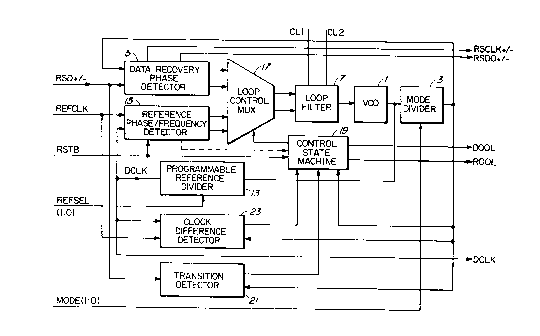
Figure 1 is a block diagram of a clock recovery
circuit incorporating the present invention,
Figure 2 is a logic diagram of an embodiment of
the clock difference detector, and
Figure 3 is a flow chart of the process carried
out by the state machine.
DETAILED DESCRIPTION OF THE INVENTION
The preferred embodiment of the clock recovery
method and apparatus described below is directed to a
clock signal of 622 Mbit/s (or 311 Mbit/s or 155
Mbit/s), as is typically used in a synchronous optical
network (SONET) system, although the invention is not
restricted thereto.
The basic phase locked loop is comprised of a
voltage controlled oscillator (VCO) 1, the output of
which is applied to the input of a mode divider 3, the
output of which is connected to the input of a phase
detector 5, the output of which is connected to the
input of the VCO through a loop filter 7. The output of
the phase detector is connected to the loop filter
through a multiplexer, to be described in more detail
below. An input data signal RSD (referred to below as
the input data signal) from which the clock is to be
recovered is applied to another input of phase detector
5.
In a successful prototype of the invention,
an embodiment of which is shown in Figure 1, the VCO
operates at 622 MHz and should have an operating range
7
X150860
sufficiently wide that it will always achieve 622 MHz
over process, temperature and voltage variations. The
operating frequency of 622 MHz should be its center
frequency, and it is preferred to have an operating
range of several hundred MHz. It should also be
optimized for low intrinsic fitter generation. In a
typical system, the maximum operating frequency of the
VCO would be less than 900 MHz under all operating
conditions.
The mode divider 3 divides the 622 MHz output
signal of the VCO by 1, 2, 4 or 12 to produce a 622,
311, 155 or 51 MHz clock that is used for data recovery
purposes, and thus for configuring the system for
recovery or synthesis of a 622, 311, 155 or 51 MHz clock
signal. The divide ratio is selected and controlled
externally by a MODE(1:0) control signal applied to a
control input of the mode divider, which can select one
out of four divide ratios using control bits 11,10,01 or
00.
The loop filter 7 integrates up or down pulses
received at its input, to generate a voltage used to
control the VCO 1. The loop filter should be designed
for low intrinsic fitter generation and to provide a
transfer function that permits adequate fitter tolerance
during clock recovery and adequate reference fitter
attenuation during clock synthesis.
The phase detector 5 is a data recovery phase
detector, which generates up or down pulses based on
comparisons of the phase of input data transitions of
the serial input data stream and transitions in the
divided down recovered clock output from the VCO and the
mode divider. It should have the characteristic that if
the serial data input stream is scrambled (i.e. pseudo-
random with 50~ ones bit density, and its bit rate is
within 122 ppm of the divided down VCO output clock
8
210860
frequency, then the data recovery phase detector should
correctly drive the loop filter and the VCO toward a
true lock condition.
Recovered clock and data signals RSCLK and RSDO
from the phase locked loop are output from the phase
detector 5 in a well known manner, e.g. by sampling the
serial data stream in the center of its eye and
generating phase aligned clock and retimed data outputs
RSCLK and RSDO.
General operation of the above circuit is well
known. The phase detector 5 detects phase difference
between the divided output signal from the VCO and the
input data signal, and provides up or down pulses,
carried through filter 7, to the VCO, which adjusts its
phase or frequency until no further up or down pulses
are generated. This basic phase locked loop would
suffer from the false locking problem described earlier.
A programmable reference divider 13 receives
the 622 MHz output signal from the output of the VCO and
divides it by 8, 12, 16 or 32 to produce a 77, 51, 38
or 19 MHz clock signal DCLK. The divide ratio is
selected externally by a two bit signal REFSEL(1:0),
which is applied to a control input of the divider 13.
The divider 13 should produce a 50% duty cycle output
signal and should be able to operate well above 622 MHz
to ensure that control is maintained over the VCO at all
times. Preferably the divider should be designed to
operate above the maximum operating frequency of the
VCO, which is indicated above to be around 900 MHz. If
this is not possible, forced low frequency startup can
be used.
A reference phase/frequency detector 15
receives at one input the DCLK output signal of the
reference divider 13 and at another input a reference
clock signal REFCLK. This detector compares the signals
9
2mosso
at its inputs, and generates up or down pulses that are
fed to the loop filter in place of the pulses output
from phase detector 5. These should always drive the
VCO to a true lock condition to the reference clock
REFCLK, regardless of the operating frequency of the
VCO. This detector 15 should be a true phase/frequency
detector.
Detector 15 may also contain circuitry to
detect an out-of-lock condition, which replicates the
phase/frequency detector 15 circuitry but with delays
inserted such that there exists a dead band. The
purpose of the dead band is to have pulses only
generated when the input signals are significantly out
of phase alignment. The up and down signals are then
logically ORed to create an out of lock signal.
When the system is reset (the reset signal not
being shown), the phase/frequency detector 15 is forced
to generate down pulses. These pulses are fed to the
loop filter 7 where they are integrated, and as a result
force the VCO to its lowest frequency.
The output signals from phase detector 5 and
phase/frequency detector 15 are applied to inputs of
loop control multiplexer 17. Depending on the value of
an input signal to its control input C, received from a
control state machine 19 to be described below, either
the up and down pulses from detector 5 or those from
detector 15 pass through and are applied through loop
filter 7 to VCO 1.
A transition detector 21 receives the output
signal from the mode divider 3 and the input signal RSD,
and determines whether the input signal transition
density is adequate for clock recovery purposes. The
transition detector provides an indication signal to the
control state machine 19 if no transitions are present
for a preferred interval of 80 bits.
The transition detector can be comprised of a
counter which counts successive bit intervals with no
transitions, which counter can be a 7 bit counter that
counts up to 80 and is reset upon the existence of a
transition. The threshold of a count of 80 is preferred
since this is the standard loss of signal threshold
specified for the SONET standard.
Upon reset, the transition detector indicates
that transition density is inadequate, until it
completes its processing interval and determines
otherwise.
Clock difference detector 23 receives and
compares the frequencies of the reference clock signal
REFCLK and the output signal DCLK of the reference
divider 13. Comparisons should be done over 8192 cycles
of the DCLK signal to establish a processing interval.
In each such interval, the number of DCLK cycles should
be counted. If this count differs by more than 1, it
should generate a signal which is applied to the control
state machine 19 which indicates that the REFCLK and
DCLK signals differ by more than 122 ppm (relative to
REFCLK). Otherwise it should generate a signal which is
applied to the control state machine 19 which indicates
that REFCLK and DCLK differ by 122 ppm or less.
The clock difference detector can be
implemented by the circuit illustrated in Figure 2. Two
13 bit counters are used in an embodiment of the clock
difference detector. The signal DCLK is divided by 8192
preferably using a ripple divider 29. Since the divided
down signal must be synchronized to REFCLK this
asynchronous design practice is safe. Three series
connected flip-flops 30A, 30B, 30C and a NOR gate 31 are
used for synchronization with REFCLK and to detect the
rising edge of the DCLK divider output. The output of
the NOR gate is one REFCLK interval wide and occurs once
1 1
~~~~gfi~
every 8192 DCLK periods. This signal pulse causes
sampling of the output of a COUNT_DEC block 33 by flip
flop 35 and clears reference clock counter 27.
The reference clock counter 27 is formed by an
iterated CNTBIT instance, such as a synchronous binary
up counter with clear and scan inputs. If the DCLK and
REFCLK clock frequencies are equal the reference counter
27 will count from 0 to 8191. The output of NOR gate 31
synchronization pulse will be aligned to a count of
8191. To allow for movement of the synchronization
position due to synchronization slips and slight
frequency differences, the synchronization pulse can
also be aligned to a reference count of 8190 or 0. The
COUNT DEC block declares the DCLK and REFCLK frequencies
to be "IN RANGE" when the reference count at the
synchronization position is 8190, 8181, 0 (nominal count
+/-1) Since the reference counter 27 is cleared at the
beginning of each integration interval the clock
frequency difference must result in a nominal count +/-2
to be detected as out of range. Due to synchronization
errors, an out of range frequency difference is first
detected when the clock frequency difference is greater
than one part in 8192 or 122 ppm.
The two flip flops 35 and 37 and an AND gate 39
are used to hold the "IN RANGE" state between
integration interval sampling points and to detect if
the reference count has been in range for two
consecutive integration intervals. If the reference
count is out of range for even one integration interval
both INRANGE1 and INRANGE2" outputs are deactivated.
An acceleration mode can be provided to make
functional simulations practical. When the ACCELB input
pin is active low, the DCLK ripple counter 29 is tapped
at the ninth bit position and the "IN RANGE" count
B
12
values are changed to 510,511 and 0. The integration
period is thus reduced to 512 DCLK cycles.
To allow for high fault coverage testing of the
gates inside the COUNT DEC block 33, a scan test chain
can be added to the reference counter. The reference
counter state can be easily controlled via a serially
shifted in pattern. This is useful since a set of
walking one and walking zero patterns is required to
detect all the "stuck at pin" faults inside the
COUNT DEC block 33.
In a successful prototype, after the analog VCO
voltage stabilized as determined by the charge pump
average current and loop filter components, at least two
integration periods were required to enter the "Locked
to Data" state. These integration periods are
summarized in the following table:
Reference Frequency Two Integration Periods
19.44 MHz 843 us
38.88 MHz 421 us
51.84 MHz 316 us
77.76 MHz 210 us
Control state machine 19 determines whether
clock is recovered from the input data or is synthesized
from the reference clock, and controls the loop control
multiplexes 17. The control state machine receives the
reset signal RSTB, a signal from the reference
phase/frequency detector 15, a control signal from the
transition detector 21 and a control signal from the
clock difference detector, and generates state machine
signals as described below. It also synchronizes the
release of reset. Its inputs are considered to be
synchronous to the high speed clock provided by the mode
divider, which also clocks the control state machine.
'.~",'-~r~
13
The clock difference detector could
alternatively be comprised of a 13 bit counter which
counts 8191 DCLK cycles and then rolls over. In this
embodiment, at the beginning of each interval, the
up/down counter should be reset to 0. Input REFCLK and
DCLK signals are monitored. On each rising REFCLK edge,
the up/down counter should be incremented. On each
rising DCLK edge, the up/down counter should be
decremented. Simultaneous rising edges should result in
the up/down counter remaining at its previous value. At
the end of each interval, the output of the up/down
counter should be sampled and then reset to 0 to begin
the next processing interval. If the up/down counter is
in a state other than 0, +1 or -l, then a clock
difference should be flagged.
The interval of 8192 cycles is used in this
embodiment because when the aforenoted clock difference
is detected, this indicates that the DCLK and REFCLK
signals differ by more than 122 ppm.
Upon reset the clock difference detector will
indicate that a clock difference exists, until it
successfully completes a processing interval which
determines otherwise.
With reference to the flow chart shown in
Figure 3, the four states of the control state machine
are 10 (reset), 11 (locked to reference), O1 (training
to data) and 00 (locked to data).
Upon release of reset, the control state
machine enters its reset state. In this state the loop
control multiplexer forces the VCO 1 to be controlled
from the output of the reference phase/frequency
detector 15. The VCO is driven until it becomes locked
to the appropriate multiple of the reference frequency.
This may be detected by the reference phase/frequency
detector which notifies the control state machine by the
14
2~~0~~0
INRANGE1 or INRANGE2. These signals are synchronous
with the reference clock that is provided to the control
state machine. The control state machine then declares
the circuit to be locked to reference. This occurs when
the divided down VCO clock and the reference clock input
differ in frequency by less than 122 ppm, as determined
by the clock difference detector 23. The control state
machine enters the locked to reference state.
If sufficient data transitions are present on
the input data, and the frequency difference remains in
range, then the control state machine should enter the
training to data state (looking for data). Once in this
state the loop control multiplexer is switched by the
control state machine to apply the output of the phase
detector 5 to the VCO 1 through loop filter 7, forcing
the VCO to be controlled by the output of the data phase
detector 5.
At this point the clock difference detector is
enabled to determine if lock is achieved. Once several
clock difference detector processing intervals are
completed, if a clock difference is not detected, the
control state machine declares the circuit to be locked
to data.
In order to enter the locked to data state,
there must be sufficient data transitions present and
the clock difference must be within range for a second
integration period to ensure that the data recovery loop
has stabilized. Once in the locked to data state the
data recovered from the RSDO and the RSCLK outputs may
be considered valid.
If the clock difference detector finds a
difference, or if the transition detector indicates loss
of signal (80 bit intervals without a transition), then
the control state machine should toggle the loop control
multiplexer 17 forcing the VCO to be controlled by the
reference phase/frequency detector. The control state
machine is also forced to be out of lock to data and out
of lock to reference, and the process begins again as if
the circuit had just been released from reset.
In the event sufficient data transitions are
lost, the control state machine should transition back
to the locked to reference state, and wait for data
transitions to be restored. In the event the
continually monitored clock difference goes out of range
due to a false lock condition, the control state machine
will transition back to the reset state and begin again
the entire process of locking to the reference clock
input signal, as described above.
The clock difference detector constrains the
VCO to a narrow range of frequencies about the
appropriate multiple of the reference frequency. In
this example where the boundary is +/- 122 ppm, this
allows the use of a low cost, readily available
reference crystal oscillator to generate the REFCLK
signal. Accuracy of +/- 100 ppm is a readily achievable
crystal oscillator tolerance.
For SONET applications in which the present
invention can be used, compliant SONET data streams must
operate at a +/- 20 ppm accuracy. Thus any deviation of
+/- 122 ppm from a reference accuracy to +/- 100 ppm or
better is a clear indication that a legal SONET signal
is not present. With such an offending signal, the
clock recovery circuit described herein will toggle
between locked to reference and looking for data, while
maintaining essentially a "keep alive" clock output for
downstream circuitry which never deviates more than
+/- 122 ppm from the reference.
As alternatives to the above-described
embodiment, a lock detect circuit could be used to
determine when it is locked to reference. As another
~, ::..;,~
16
alternative, the clock difference detector can be used
to check for lock to reference in a manner analogous to
using the clock difference detector to check for lock to
data.
Either the REFCLK or DCLK can be used as the
timebase for implementing the processing interval of the
clock difference detector. When implementing the
counters which integrate the clock difference, small
saturating counters could be used (which do not truly
indicate the clock difference if significant fitter and
wander is present on the REFCLK or DCLK signals due to
information being lost when the counters saturate).
Alternatively, longer counters can be used which perform
integrations that are accurate under all situations.
Further, a longer processing interval or different
counter thresholds so as to constrain the maximum
allowable clock difference to be less than or greater
than +/- 122 ppm can be chosen for the implementation.
A person understanding this invention may now
conceive of alternative structures and embodiments or
variations of the above. All of those which fall within
the scope of the claims appended hereto are considered
to be part of the present invention.
17