Note: Descriptions are shown in the official language in which they were submitted.
21135 6
1
The present invention concerns a pre-distorting
linearization circuit, comprising a splitter circuit with
an input forming the input of the linearization circuit
and first and second outputs feeding first and second
parallel stages respectively, of which at least one has a
defined distortion characteristic, and a combining
circuit receiving the signals provided by the first and
second stages at first and second inputs respectively and
having a recombination output which forms the output of
the linearization circuit.
Such a circuit, which is known as a circuit with a
bridge configuration, provides great flexibility and
avoids operating the circuit in conditions of high
distortion.
One simple bridge circuit thus splits the signal
into two components having a phase difference
therebetween of 90° or 180°, using a power divider. One
of the signals is then treated by a linear branch forming
the first stage and the other signal by a non-linear
circuit forming the second stage. The phase and
amplitude of the signal are not altered in the linear
branch. However, the phase and amplitude are modified in
the non-linear branch. The two signals are then combined
with suitable amplitude and phase, obtained with an
attenuator and a phase shifter for example, in a
combining circuit which is in general of the same type as
the circuit used to split the input signal. The result
of this treatment is that the signal presented to the
input of the linearization circuit can have gain
expansion and a delay, or even an advance, which can be
made complementary to those of the transmitter which is
to be linearized.
Such a pre-distorting linearization circuit can be
used in particular for satellite transmissions involving
a plurality of carriers. It is an object of the
invention to allow the power amplifiers used for this
2151356
2
transmission to operate closer to their saturation
characteristics, which improves their efficiency and thus
their functionality. Such a consideration is equally
applicable to transmitters for amplifying signals with a
non-constant envelope, for example with filtered QPSK
modulation, i.e. quadrature modulation with phase shift.
Pre-distorting linearization circuits are used in
preference to linearization circuits of other types
because of their efficiency, their simplicity, and their
low losses, and also because they do not introduce
attenuation into the output signal.
A pre-distorting linearization circuit can also be
useful in distributed antenna systems (array, multi-port
systems, etc.) in order to increase linearity and at the
same time reduce the phase and gain tracking demands
between the different amplifier units.
A pre-distorting linearization circuit is generally
located between the amplifier of the corresponding
channel and the traveling wave tube amplifier, or is even
integrated directly into an integrated power amplifier,
to form an amplifier module. Its function is to provide
amplitude and phase characteristics which complement
those of the transmitter, so as to compensate for
distortion.
The end result which can be achieved with this
linearization is that the transmitter can be operated
very close to its saturation region while preserving
satisfactory nominal linearity.
Known types of linearization circuits which are in
the form of a bridge generally have a linear branch
formed by a simple connection, by a phase shifter and/or
by a variable attenuator or even an amplifier. The non-
linear branch is implemented by a component which
introduces distortion, e.g., a PIN or Schottky diode or
even MESFET type field effect transistors with a single
or double gate.
215~35fi
- _
3
One of the important parameters of linearization
circuits is the amplitude ratio of the bridge, i.e. the
ratio between the two output signals of the two branches.
Ideally this ratio should be as close as possible to
0 dH.
The present invention concerns a pre-distorting
linearization circuit which is to be simple in its
architecture and allow an amplitude ratio of the bridge
to be maintained easily, without introducing attenuation
of the signal.
The concept is based on making use of the
characteristics of transistors in the two branches in
such a manner that they impart different non-linearity
properties. In particular the invention relies on the
possibility of implementing different sizes of MESFET
type transistors in microwave monolithic integrated
circuits (MMICs).
The linearization circuit of the invention is thus
characterized in that the first and second stages have
first and second transistors respectively having
- different dimensions, which confer different non-
linearity characteristics thereon, such that for the same
voltage on the input of the linearizatzon circuit, the
first stage exhibits a higher degree of non-linearity
than the second stage.
In a preferred embodiment, the first and second
transistors are field effect transistors, in particular
of MESFET type, having first and second gates
respectively, whose widths are in a given ratio other
than unity; this ratio may for example lie in the range 2
to 10 and is preferably equal to 4. Each of the MESFETs
advantageously has separate gate bias and drain bias
terminals, thereby enabling their distortion
characteristics to be adjusted more finely.
It is an advantage if the splitter circuit and the
combining circuit have a nominal impedance of 100 S~. To
this end, the splitter circuit and the combining circuit
21513~~
4
can have a series branch comprising in succession a
first, a second, and a third capacitor in series, forming
an output branch for the splitter circuit and an input
branch for the combining circuit, a first inductor having
a first terminal connected to a first terminal of the
second capacitor, a second inductor having a first
terminal connected to a second terminal of the second
capacitor, a fourth capacitor connected between the
second terminals of the first and the second inductor and
a resistor connected between the second terminal of the
second inductor and a voltage supply terminal, generally
ground, the second terminal of the first inductor forming
an input terminal. for the splitter circuit and an output
terminal for the combining circuit.
The first stage can have a phase shift component,
for example a delay line. The splitter circuit, the
combining circuit and the first and second stages are
preferably on a first substrate of MMIC technology, while
the delay line is on a second substrate of MIC technology
(microwave integrated circuit).
In the accompanying drawings:
- Figure 1 is a block diagram of a pre-distorting
linearization circuit of bridge type with two branches of
the prior art;
- Figure 2 is an illustration of the operation of
the linearization circuit of Figure 1;
- Figure 3 is a block diagram of a splitter circuit
or a combining circuit with a nominal impedance of 50 S~
of the prior art;
- Figure 4 shows a preferred embodiment of a pre-
distorting linearization circuit of the present
invention;
- Figure 5 shows a variant of the circuit of
Figure 4 implemented on two substrates;
215135fi
- Figures 6a to 6e represent the non-linearity
characteristics of the circuit of Figure 4 as a function
of different adjustments of the delay line corresponding
to phase shifts of respectively 0° (reference), 10°, 20°,
5 30° and 40°;
- Figure 7 shows the characteristics of the response
curves for the "small signal" mode between 11 GHz and
14 GHz corresponding to the case of Figure 6d;
- Figures 8a and 8b are curves showing the
adjustments possible for two values of the gate and drain
voltages of the circuit of Figure 4, these values lying
between 1.5 V and 3.5 V for VD1 and VD2 and between
-0.5 V and -1.5 V for VG1 and VG2.
The pre-distorting linearization circuit of the
prior art shown in Figure 1 is of simple bridge type. In
this the input signal Vi is split by a splitter circuit
DIV into two signals with a phase difference of 90° or
180° between them. One of these signals is treated by a
stage forming a first branch B1, which is a non-linear
branch, while the other signal is treated by a second
stage forming a second branch B2, which is a linear
branch, i.e. a branch in which the amplitude and the
phase of the signal are not modified. In the non-linear
branch B1 the amplitude and the phase of the signal are
modified, after which the two output signals of the two
branches, denoted V1 and V2, are fed with the required
amplitude and phase into a combining circuit COM, which
is in general the same as the splitter circuit DIV, but
operating with the inputs and outputs reversed. It is
noted that the first branch B1 comprises a phase shift
circuit DEPH (and possibly an attenuator ATT), which
allows the desired amplitude and phase of the signal V1
to be obtained. The output signal VO of the pre-
distorting linearization circuit which will be applied to
the input of the transmitter has gain and phase
characteristics which are complementary to those of the
transmitter, so as to compensate for its distortion.
2151356
6
This compensation for distortion is illustrated in
Figure 2, in which the vector V2 has its amplitude
multiplied by 2 at the output of the linear branch B2,
while the vector V1 at the output of the non-linear
branch B1 is subjected to a phase advance of 30°, for
example, and has its amplitude multiplied by a factor
less than 2, for example 1.5, because of the compression
of the corresponding level by its non-linear
characteristic. If the phase and amplitude of the
signals V1 and V2 are correctly adjusted, the vector
representing the output signal VO of the bridge circuit
has an increase in amplitude (expansion of level) as well
as a phase advance. It is important to note that, for
efficient linearization, the amplitudes of the linear
vector and the non-linear vector at the outputs of the
linear and non-linear branches, i.e. the signals V1 and
V2, should be similar, as has been mentioned above. The
amplitude ratio between the two signals, normally called
the amplitude ratio of the bridge, generally lies in the
range 0 dB to -4 dB.
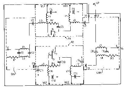
Referring to Figure 4, the linearization circuit of
the invention is of the general type shown in Figure 1,
comprising a splitter circuit DIV and a combining circuit
COM, which can be of the known type shown in Figure 3 or
equally, as is shown in the course of the description, of
the type shown that corresponds to a nominal impedance of
100 D.
The two branches B1 and B2 comprise field effect
transistors of MESFET type, T1 and T2 respectively,
connected as source followers. The gates G of the
transistors T1 and T2 are connected to the respective
outputs of the splitter circuit DIV through respective
series inductors L3 and L9 and their drains D are
connected to the respective inputs of the combining
circuit COM through respective inductors L6 and L12. Each
of the transistors T1 and T2 has a gate bias circuit,
namely with a series inductor L4 and a shunt capacitor C4
21513~fi
to ground for an adjustable gate voltage terminal VG1 for
the branch H1, and a series inductor L10 and a shunt
capacitor C12 for an adjustable gate bias voltage
terminal VG2 for the branch B2. Likewise, in order to
bias the drains of the transistors T1 and T2, there is a
similar arrangement, namely an inductor L5 and a
capacitor C6 for an adjustable drain voltage terminal VD1
for the transistor T1 in the branch B1 and an inductor
L11 and a capacitor C14 for an adjustable drain voltage
terminal VD2 for the transistor T2 in the branch B2. In
addition, a resistor and a capacitor in series provide
drain-gate feedback, namely R2 and C5 for the transistor
T1 and R4 and C13 for the transistor T2.
The transistors T1 and T2 are MESFETs with different
gate widths, this gate width being smaller for the
transistor T1 in the non-linear branch B1.
The invention uses one of the possibilities allowed
by MMIC technology, namely dimensioning individual
components (transistors, inductors, capacitors,
resistors, etc.).
- In the case of the MESFETs, this dimensioning is
effected by determining the gate width GW. In the case
of a MESFET, the output power PO is directly related to
the gate width GW (expressed in mm) by the linear
equation:
PO = KGW
The constant K (in W/mm) is the power density and
its value is a characteristic of the MMIC technique
employed, and the value of K varies little as a function
of the frequency of operation. The value of K is
substantially equal to 0.5 W/mm for power MMIC methods
around 10 GHz and is in the order of 0.2 W/mm or even
less for low noise methods or general usage.
In the pre-distortion bridge circuit of the
invention, transistors T1 and T2 of different sizes are
implemented in the branches B1 and B2 so that a
transistor T1 of small size in the non-linear branch B1
_2151356
8
and a transistor T2 of greater size in the linear branch
H2 make it possible for the transistor T1 to operate in a
non-linear range, while the transistor T2 of greater size
operates in its linear region, for a certain range of
input power values. A transistor is considered by
definition to be in its linear region when its departure
from linearity corresponds to compression of less than a
given relative value, 1 dB for example.
If for example the transistor T1 has a gate width G1
four times smaller than the gate width G2 of the
transistor T2, it exhibits in its output power
characteristic an output power with 1 dH compression,
which will be approximately 6 dH lower than that of the
transistor T2.
The more the ratio between the gates widths is
increased, the greater the input power range over which
the linearization circuit is able to provide
compensation, but it also results in the circuit
consuming more continuous power. This input power range
in which compensation is possible is limited by the
compression characteristics of the transistor T2 and by
the maximum allowable input power for the transistor T1
compatible with reliable operation thereof.
In practice the ratio G2/G1 lies in the range 2 to
10 and the preferred value is 4.
It is noted that the presence of a MESFET in each of
the two branches of the bridge also provides another
important advantage. Thus, these transistors provide
gain in each of the branches, which keeps the amplitude
ratio of the bridge at a value close to 0 dB, which
allows maximum linearization efficiency. It is noted
that this is not the case for example in prior art
bridges in which passive components, e.g~ PIN diodes,
are used to introduce the distortion. When the branch
introducing distortion also produces attenuation, this
attenuation has also to be introduced into the linear
branch, so as to obtain the best linearizaticn
_2151356
9
efficiency, which results in needless increase in the
losses in the linearization circuit.
An important feature of the linearization circuit is
the selection of the network forming the splitter circuit
and the combining circuit. This can be a conventional
network with a nominal impedance of 50 D, e.g. is
shown in Figure 3, which has two branches, each with
three capacitors in series, namely C21, C0, C22 for the
first branch and C23, C20 and C24 for the second branch.
An inductor L20 is connected between the terminal common
to the capacitors C21 and CO and the terminal common to
C23 and C20. An inductor L21 is connected between the
terminal common to the capacitors CO and C22 and the
terminal common to C20 and C24. Furthermore, a resistor
RO is connected between the terminal common to the
capacitors CO and C22 and ground. The terminal common to
the capacitors C21 and CO forms the input E in the case
of a splitter circuit DIV and the output S in the case of
a combining circuit COM. The terminal common to the
capacitors C23 and C20 forms a first output S1 in the
case of a splitter circuit DIV and a first input E1 in
the case of a combining circuit COM. Likewise the
terminal common to the capacitors C20 and C24 forms a
second output S2 in the case of a splitter circuit DI'J
and a second input E2 in the case of a combining circuit
COM.
By way of example, we have:
C21 = C22 = C23 = C24 = 0.1 pF.
CO = C20 = 2C21
L20 = L21 = 0.45 nH
In a preferred embodiment of the present invention,
which is shown in Figure 4, the splitter circuit DIV and
the combining circuit COM have a nominal impedance of
100 ~. This allows the number of capacitors required to
be halved. Furthermore, the capacitors next to the dual
output port of the circuit DIV or the dual input port of
the circuit COM can be buried under the coupling networks
215135
of the linear and non-linear amplifiers, which enables
the area of gallium arsenide occupied by the integrated
circuit MMIC to be reduced.
As shown in Figure 4, the splitter circuit DIV has
5 an input terminal E which is the point common to an
inductor L1 and a capacitor C1. The other terminal of
the capacitor C1 is connected firstly to a first terminal
of a resistor R1 with a value of 50 t~, the other terminal
of which is grounded, and secondly to a first terminal of
10 the inductor L2. The capacitor C2 is connected between
the second terminals of the inductors L1 and L2.
Capacitors C3 and C10 are connected, the former between
the second terminal of the inductor L1 and the inductor
L3 and the latter between the second terminal of the
inductor L2 and the inductor L9. The combining circuit
COM is formed in the same way, the capacitors C1, C2, C3
and C10 being replaced by the capacitors C9, C8, C7 and
C16 respectively, the inductors L1 and L2 by the
inductors L7 and L8 respectively and the resistor R1 by
the resistor R3.
It is also noted that the circuit has two terminals
X1 and X2 for connection to an external delay line LR,
these terminals being interposed between the capacitors
C7 and C8.
By way of example, we have:
C3 = C2 = C6 = C7 = C8 = C16 = 0.125 pF
C1 = C9 = 0.25 pF
L1 = L2 = L7 = L8 = 0.63 nH
Rl = R2 = 50 S~ .
According to the invention, the phase is set in the
non-linear branch B1 by means of a delay line LR with a
nominal impedance of 100 t~ corresponding to that of the
circuits DIV and COM. In order to be able to match
different required linearization characteristics, the
delay line LR is preferably disposed not on the MMIC chip
containing the linearization circuit proper but outside
it on an alumina substrate 2 which is used for assembling
215135fi
11
the chip 1 to form a module. This is shown in Figure 5.
The length of the line is modified by altering the number
of unit connecting terminals 5 which are connected in
series by conductive links 3.
It is noted that, in order to obtain a less
pronounced linearization action, the delay line LR can be
designed to allow attenuation of the amplitude of the
non-linear vector V1 and hence an increase in the
amplitude ratio of the bridge. This attenuation can be
obtained using thin film resistors 6 between the
terminals of the elementary connecting terminals 5 for
example, as is shown ringed in Figure 5.
The use of a delay line LR makes it possible to
avoid an increase in the complexity of the bridge
involved in use of a conventional phase shifter.
The present invention can be implemented in
particular to provide a pre-distorting linearization
circuit in MMIC technology implemented using the LN-5
process of THOMSON. This process is a MESFET process
having a characteristic gate length of 0.5 Via.
- The transistor T2 has four fingers each of which has
a length of 150 a for a total gate width of 600 u. The
small transistor T1 has two fingers of length 75 a for a
total gate width of 150 p. Distortion is thus obtained
in the linear branch which is equal to that of the non-
linear branch over a power range which is 6 dB above that
of the non-linear branch. The gain in each of the
branches is in the order of 6 dH, which keeps the bridge
ratio in the region of 0 dB for maximum linearization
efficiency and reduction of the total insertion losses of
the linearization circuit. The total power consumption
is in the order of 225 mW.
Figures 6a to 6e show the gain and phase shift of
the linearization circuit for input powers ranging from
0 dBm to 15 dBm and for increasing values of delay
created by the delay line LR.
215135
12
Figure 7 shows the response curve for small signals
ranging from 11 GHz to 14 GHz corresponding to Figure 6d,
i.e. to the case in which the maximum expansion of gain
is obtained. This corresponds to the case in which the
vectors in the linear branch V1 and the non-linear branch
V2 have approximately the same amplitudes but a phase
difference of 180°. This produces a drop of around 15 dB
in the response curve as is shown in Figure 7.
Figure 6e shows a configuration in which the
expansion in gain is in the order of 11 dB with a phase
advance of approximately 50°.
The configuration shown in Figure 4 allows the gates
and the drains of the transistors T1 and T2 to be
separately biased. This allows supplementary adjustments
of the linearization circuit. Obviously, if such
adjustments are not required, the transistors T1 and T2
can be biased by predetermined, fixed bias voltages.
Figures 8a and 8b show the changes in the
characteristics which can be obtained by separately
adjusting the drain voltage (VD1, VD2) and the gate
voltage (VG1, VG2) of the transistors T1 and T2. In
particular it is possible to obtain a phase delay or a
phase advance while maintaining expansion in gain.