Note: Descriptions are shown in the official language in which they were submitted.
- ~ 21~185~
Hot-clock adiabatic qate usin~ multi~le clock siqnalQ with
different ~hases
R~CK~OUND OF THE lNv~NllON
FIELD OF THE lNV ~:N'l'lON
The present invention pertains to low-power
semiconductor circuitry. More particularly, the present
invention pertains to complementary transistor gates for
adiabatic circuits.
DISCUSSION OF RELATED ART
Circuits that operate with low power requirements are
_ desirable for use in many electronic devices, particularly
portable devices that are powered by batteries, solar
cells, or other limited-capacity power supplies. One of
the advantages of CMOS circuitry has been its low rate of
power dissipation relative to emitter-coupled logic (ECL),
bipolar, and other types of semiconductor circuit devices.
However, even as mask technology reduces the size of
CMOS structural elements to the submicron range, these
elements are increasingly called upon to perform their
switching functions at the high end of the frequency
spectrum. As a result, some recent CMOS circuit designs
have wattages more appropriate for the common lightbulb
than for submicron, heat-sensitive ~LSI semiconductor
packages.
Generally, the energy dissipated in switching can be
reduced to provide adiabatic performance if logic switching
is performed quasi-statically: the dissipation of energy
through a dissipative medium is reduced if the transfer is
made gradually enough. Despite their name, so-called "hot
clock" circuits are unconventional circuit designs that
apply this principle to provide adiabatic performance.
These devices reduce the rate of change in the circuit, but
"gradually" is a relative concept. Known "hot clock"
circuits are capable of operating at frequencies as high as
20 MHz in 0.9 micron CMOS. Under these conditions a 5x to
10x power dissipation reduction can be achieved by hot-
clock designs.
21S18~1~
-
- 2
Hot-clock logic designs supply all power to the gates
via their clock lines, as described by Seitz, et al. at the
Chapel Hill VLSI Conference in 1985. Quasi-static logic
operations have two cardinal rules, rules familiar to those
in the DC to DC converter art: (1) Never enable a switch
unless the potential across it is zero; (2) Never disable
a switch if there is a current flowing through it.
Hot-clock circuit performance in CMOS has been
improved by adding blocking diodes, as disclosed by Avery,
et al., in Serial No. 08/175,709 filed 12/30/93. However,
the resulting circuit may require that clock levels be
~- boosted asymmetrically, or that level shifters be provided
between gates or low-threshold diodes be used to overcome
the resulting diminished signal voltage swings at the
circuit's output.
.
SUMMARY OF THE lNv~N-llON
A CMOS gate in accordance with the present invention
includes a gate transistor pair, an output node between the
gate transistors in the pair, and a pair of gate clock
signals. Each gate clock signal is connected to the source
electrode of a respective CMOS gate transistor.
An ancillary transistor preferably has its channel
adapted for connection to the drain of each gate transistor
and the output node. A respective one of a pair of
complementary ancillary clock signals is connected to the
gate electrode, the "control element" of each respective
ancillary transistor. Said ancillary clock signals are
phase-shifted from the gate clock signals so that said four
clock signals have four distinct phases, whereby the gate
transistor pair is enabled to establish and maintain full-
rail voltage values at the output node. Preferably, these
four clock signals are phase-shifted a full 90 degrees from
each other.
In particular, the ancillary transistors and offset
clock signals of the present invention provide adiabatic
performance while producing full-rail voltage swings at
21~i85~
~ - 3 -
- gate outputs. In a preferred embodiment this is achieved
in homogeneous CMOS device packages. Homogeneous packages
are simpler to fabricate than the composite packages
required for circuits that include functions such as output
level shifting or an asymmetric boost on the clock leads.
In particular, the Schottky diodes that are preferable for
use as blocking diodes are non-MOS devices and their use
can be avoided, for many applications, in accordance with
the present invention.
In another embodiment the interaction of blocking
diodes with offset clock signals in accordance with the
--- present invention provides a further reduction of non-
adiabatic device charging in a circuit, for specially
demanding applications.
BRIEF DESCRIPTION OF THE DRAWINGS
The features and advantages of the present invention
will be better understood when the detailed description of
a preferred embodiment given below is considered in
conjunction with the drawings provided, wherein:
Fig. 1 is a diagram of a prior art logic circuit;
Fig. 2 is a timing diagram for the circuit of Fig. 1;
Fig. 3 is a diagram of a CMOS logic circuit in accor-
dance with a first embodiment of the present invention;
Fig. 4 is a timing diagram for the circuit of Fig. 3;
Figs. 5a through 5c are diagrams of other types of
logic gates in accordance with the present invention;
Fig. 5d is a schematic diagram of a memory cell that
incorporates ancillary transistors controlled by multiple
clock signals of different phases, according to the
principles of the present inventioni
Fig. 5e is a graph illustrating the amplitude and
relative phase of multiple clock signals, which are
preferably applied to the memory cell circuit illustrated
in Fig. 5d; and
Fig. 6 is a timing diagram for the circuit of Fig. 3,
showing a different input signal In.
- -: 21S18SO
~ 4 -
Li~e~:reference numerals indicate like structures.
D~T~T~-~n ~ RTPTION OF T9~ ~n~A~ E~_OD$NENT~
Fig. 1 shows a string of CMOS inverters using two
offset trapezoidal "hot clock~ signals C~ and C~, and their
complements, to obtain A~; AhAtiC operation. In Fig. 2, it
can be seen that output waveforms A, B and D do not swing
n full rail n through the full voltage range V" - V~ in
response to full-rail swings in the input signal In.
In the Fig. 1 circuit, the input signal that is
supplied to the control element of each gate transistor
changes during a 8ET~P P~A8~ -(#1) when the clock signal
input to that gate has been entirely disabled, as required
for adiabatic operation, and the gate's output floats, as
indicated by the ~Aehe~ line. Hos~e~e-, the gate's output
is, by then, alreadY floatina in midranae rather than
holding the full logic values V~ and V~.
For example, in Fig. 2, when Cl goes high during the
E~a~L~ P~A8~ ~#2), NNl becomes enabled and output A makes
the transition to full V~ and holds that value. However,
hecAI~-ee the clock signal is trapezoidal, during the nT~RT-
~P~A8T (#4) gate transistors ~Pl and ~n being disabled, and
- the active gate transistor ~1 rPm~;ne active long enough to
permit a current to pass through ~Dl, causing the output A
to follow the clock C~ to a mid-range voltage. Then, MNl
finally becomes disabled, and the output A floats at
midrange during the rest of the nT~r-.~ P~A8T (#4) rather
than hold its full-rail value of Vg8. The output A
continues to float during the subsequent g~T~P P~A8~ (#1),
when the gate transistors have completed their transitions
and the path between C~ and its complement C~ is once again
cut off.
The input signal I~ in this t;m;n~ diagram changes
value from V~ to Vs,, or VgJ to V~ during the g~T~P PHAS~
(#1). In the ~RT-~ PHAgE (#2), that full-rail change in
2 1 ~
~_ 5
- the inp~-t signal I~ during the ~T~P P~A8E (#l) produces a
belated, partial change in the output signal A from midrange
to a full V~ or ~g, value in the ~N~RL~ P~AgF (#2). This
distorted signal appearing at the output of the gate A then
propagates through the rest of the inverter gates B, D and
Out, in this orderly but unsatisfactory fashion.
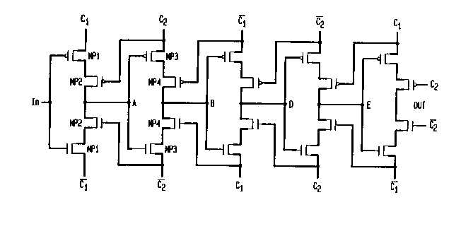
Fig. 3 shows another serial string of inverters that
provides full-rail signal transitions and improved ~;AhAtic
performance in accordance with a first emhoA;ment of the
present invention. Again, each pair of gate clock signals,
such as C~ and C~, is connected to the source electrodes of
-a respective pair of CMOS gate transistors NPl and MNl, and
the drain electrode of each gate transistor MPl and MNl is
connected to the gate's output node through ancillary
transistors NP2 and ~2.
However, in Fig. 3, an ancillary transistor ~P~ or MN2
is connected between each respective gate clock and the
output node. Specifically, the source elctrode of each
ancillary transistor, ~P2 and ~2 is connected to the drain
electrode of the respective gate transistor ~Pl or MNl and
the drain electrode is connected to the output node A.
Also, a respective one of a pair of complementary clock
signals C~ and C~ that are offset from the gate clock signals
of that gate, C~ and C~, is connected to the gate electrode,
the ~control element~ of each respective ancillary
tran~istor N~2 or ~2.
In Fig. 3 the gate clock pair in each stage, for
example C~ or C, and its complement, is also supplied to a
previous stage, a stage that is driven by another, offset
clock, C, or C~ respectively. This assures that the
ancillary transistors MP2 or NW2 will be cut off during the
gate's DIgAB~F P~Ag~ (#4), so that the path between the
clock signals and the output A is disrupted. In contrast to
Fig. 2, each ancillary transistor MP2, MW2 is fully cut off
while the gate transistor MPl, MWl connected in series with
21518~0
-- 6 --
it is in transition in Fig. 4, and the output A r~m~; n.C at
its full-rail value. This action of the gate~s ancillary
transistors produces a full-rail voltage swing at output A
during the subsequent ~NaB~E P9A~E (#2), as in Fig. 4.
S Fig. 5a shows a CMOS NAND gate circuit in accordance
with the present invention. Fig. 5b shows a CMOS NOR gate
circuit in accordance with the present invention. In these
logic gates the gate transistors are controlled by the input
signals r~ and IN2. Offset clock C" and its complement,
control the auxiliary transistors M~3 and ~P3, respectively.
These ancillary transistor pairs prevent the outputs A from
-- following the trapezoidal clocks by disrupting the path to
the gates~ outputs during the transistions of clock Cl and
its inverse, as in Figs. 3 and 4.
Of course, inverters and other gates in accordance with
the present invention can be connected in series as shown in
Fig. 3, or in parallel as shown in Fig. 5c, or in any
combination thereof. Also, rather than being a logic gate,
the gate may be a memory cell, as shown in Fig. 5d. In each
instance, the ancillary transistors between the respective
gate clocks and the gate output ~L~ve~t the trapezoidal
clocks from wasting power and distorting the output signal,
as expl~i n~ above.
In Fig. 7, hot-clock blocking diodes have been added to
the circuit shown in Fig. 3 to ~Lev~t the non-~ h.~tic
charging that may occur when a gate's input signal does not
change. This non~ hAtic charging ~pr~rs at the output
nodes in the Fig. 6 timing chart during each gate~s SETUP
PHASE (#l) when the input signal to the gate is flat, as a
low-level signal artifact shown in phantom.
- In Fig. 7, as in Fig. 3, the source electrode of each
ancillary transistor, M~2 and ~2 is connected to the drain
electrode of the respective gate transistor N~l or MNl and
the drain electrode is connected to the output node A.
Also, a respective one of a pair of complementary clock
- 2151850
-- 7
~ signals-C~ and C2 that are offset from the gate clock signals
of that gate, Cl and C~, is connected to the gate electrode,
the "control element n of each respective ancillary
transistor MP2 or MN2.
However, it has been found that slight non~ hAtic
charging occurs in the circuit shown in Fig. 3, when the
input signal r~m~;nC flat during the SETUP PHASE (#1). This
signal artifact is indicated in phantom in Fig. 6. In the
SETUP PHASE (#l) of the second clock period, partial non-
~ h~tic charging occurs at A through a "bump~ of about 2V
in a 5V device, caused by the enablement of ~o2 by C~ while
-- C~ is still high. This ~bump~ also occurs at A through the
enablement of NP2 by C~ while C~ is high, although the
deviation is somewhat smaller hec~l~se of an inherent
difference between the response of n-ch~nnel and of p-
~h~nn~l materials.
This rem.~; n; ng artifact can be removed by the use of
blocking diodes, while m;n;~izing the negative effects of
the blocking diodes by providing a bus for each of four
clock buses, for each symmetrical half of the CMOS circuit,
as shown in Fig. 7, rather than a diode for each gate
transistor.
This one-diode-per-bus circuit is particularly
advantageous when Schottky diodes are used, since Schottky
diodes are not MOS devices and are quite ~Yr~ncive to add to
an MOS chip. However, MOS diodes do not provide adequate
bloc~;n~ at the low voltage levels where the residual power
losse~ and signal distortions occur in this circuit. Thus,
if supplemental diodes are used in circuits operated in
accordance with the present invention they would,
preferably, be Schottky diodes.
It will be appreciated by one skilled in the art that
variations and modifications of the disclosed apparatus are
possible within the spirit and scope of this invention. For
example, the clocks Cl, C2 need not be fully 90 degrees
21~18~V
- 8 -
offset -to enjoy some of the benefits of the present
invention. The embodiments described are provided to
illustrate presently preferred ways of making and using this
invention. The invention is defined by the claims appended
below.