Note: Descriptions are shown in the official language in which they were submitted.
~ WO 95/13666 ~ 1 5 2 8 Q 9- PCT/US94/11469
APPARATUS AND METHOD E OR OPERATING A PHASE
LOC~) LOOP ~EQI~CY SYNTFIF ~ RESPONSIVE IY)
RADIO FREQUENCY CHANNEL SPAC~G
Field of the Invention
The present invention relates generally to radio
communication transceivers and, more particularly, to an
apparatus and method for operating a phase locked loop frequency
synthesizer responsive to radio frequency ~h~7nnel spacing in a
radio communication transceiver.
R~l~rol7n~7l of the Invention
FIG. 1 illustrates, by example, a block diagram of a
conventional radio communication transceiver 100 (hereinafter
~efe-~ed to as "transceiver"). The transceiver 100 enables a mobile
or portable subscriber unit to communicate with a base station
(not shown), for ~ 7mple, over radio frequency (RF) channels in a
radio commllnic~7t;on system (not shown). The base station
thereafter provides communications with a l~n~7.1ine telephone
system (not shown) and other subscriber units. An example of a
subscriber unit having the transceiver 100 is a cellular
radiotelephone.
The transceiver 100 of FIG. 1 generally includes an antenna
101, a duplex filter 102, a receiver 103, a transmitter 105, a
reference frequency signal source 107, a receive (Rx) phase locked
loop (PLL) frequency synthesi7.er 108, a transmit (Tx) PLL
frequency synthesizer 109, a processor 110, an information source
106, and an information sink 104.
The interconnection of the blocks of the transceiver 100 and
operation thereof is described as follows. The antenna 101
receives a RF signal 119 from the base station for filtering by the
duplex filter 102 to produce an RF received signal at line 111. The
duplex filter 102 provides frequency selectivity to separate the RF
rece*ed signal at line 111 and the RF transmit signal at line 113.
-
W095/13666 ~` ~15 ~ 8 ~ 9 PCT~S94/11469
-2-
The receiver 103 iæ coupled to receive the RF received signal at line
111 and operative to produce a received baseband signal at line 112
for the information sink 104. The reference frequency signal
source 107 provides a reference frequency signal at line 115. The
Rx PLL frequency synt.hçsi7.er 108 is coupled to receive the
. efe. ellce frequency signal at line 115 and information on a data
bus 118 and op~lal,iv~ to produce a receiver tur~:e signal at line 116
to tune the receiver 103 to a particular RF ~h~nnel. Likewise, the
Tx PLL frequency synthesizer 109 is coupled to receive the
reference frequency signal at line 115 and information on the data
bus 118 and operative to produce a transceiver tune signal at line
117 to tune the transmitter 105 to a particular RF ~.h~nnçl. The
processor 110 controls the operation of the Rx PLL frequency
synt.hçsi~er 108, the Tx PLL frequency synthesizer 109, the
receiver 103, and the transmitter 105 via the data bus 118. The
information source 106 produces a baseband transmit signal at
line 114. The transmitter 105is coupled to receive the baseband
transmit signal at line 114 and operative to produce the RF
transmit signal at line 113. The duplex filter 102 filters the RF
transmit signal at line 113 for radiation by the antenna 101 as a
RF signal 120.
The RF l~h~nnel~ in a cellular radiotelephone system, for
example, include voice and .~ign~ling çh~nnçls for transmitting
and receiving (hereinafter ~efe~-ed to as "transceiving")
information between the base station and the subscriber units.
The voice ~-.h~nn~ are allocated for transceiving voice
information. The sign~ling ~h~nnçl.c, also referred to as control
ch~nnel.~, are allocated for transceiving data and .~ign~ling
information. It is through these sign~ling ~h~nnel.c that the
subscriber units gain access to the cellular radiotelephone system
and are ~;gnçd a voice ~h~nnel for further communication with
the l~n~llinç telephone ~y~em. In cellular radiotelephone
systems capable of transceiving wide band data on the si~n~lin~
ch~nn~ , the frequency spacing of the .~ign~ling ch~nnel.~ is a
multiple of the frequency spacing of the voice çh~nnçl~.
In some cellular radiotelephone systems, the transceiver
100 and the base station intermittently transceive information
~ WO 9D13666 2 1 ~ 2 8 0 ~ rcr/u~94lll469
therebetween on the ~ign~ling ch~nnel One such system, for
example, an interleaved data .~ign~ling method to synchronize the
intermittent information. In this type of system, keeping the
transceiver 100 fully powered during the entire time that the
6 transceiver 100 is tuned to the æign~ling rh~nnel unnecessarily
drains the transceiver's battery during those times when the
information is not received. Thelefole, portions of the transceiver
100 can be powered off to prolong battery life when the transceiver
is not transceiving inform~t.ion. Further, portions of the
transceiver 100 can be powered off to prolong battery life when the
signal quality is good enough such that further repetition of the
same information is not needed. Intermittently powering on and
off, i.e. enabling and ~ hling, the transceiver 100 during its
receive operation is called discontinuous receive (DRX) mode of
operation. In the DRX mode of operation, quickly enabling and
hling the portions of transceiver 100 increases the savings in
battery life.
FIG. 2 illustrates, by e~mple, a block diagram of a
conventional phase locked loop (PLL) frequency synthesizer for
use in the transceiver 100 of FIG. 1. The general structure of the
PLL frequency synthesizer of FIG. 2 is the same for both the Rx
PLL frequency synt.he~i7er 108 and the Tx PLL frequency
synt.hesi7.~r 109.
The PLL frequency synt.hesi~er 108 or 109 of FIG. 2
generally includes a reference divider 201, for discussion
purposes, and a PLL 212. The PLL 212 generally includes a phase
detector 202, a loop filter 203, a voltage controlled osr.ill~tor 204,
and a loop divider 205. The reference divider 201 receives a
reference frequency signal on line 115.
The interconnection of the blocks of the PLL frequency
synt.hesi7.er 108 or 109 of FIG. 2 is described as follows. The
reference divider 201 is coupled to receive .the reference signal at
line 115 and the data bus 118 and operative to produce a divided
reference frequency signal at line 206. The phase detector 202 iscoupled to receive a divided reference frequency signal at line 206
and a feedback signal at line 209, and operative to produce a phase
error signal at line 207. The loop filter 203 is coupled to receive the
2~ 528~9
W O 9S/13666 PCTrUS94/11469
- 4 -
phase error signal 207, and operative to produce a filtered signal
at line 208. The voltage controlled oscillator 204 is coupled to
receive the filtered signal at line 208 and operative to produce an
output frequency signal at line 116 or 117. The loop divider 205 is
coupled to receive the output frequency signal at line 116 or 117,
and operative to produce the feedback signal at line 209. The loop
divider 205 and the ~efe~llce divider 201 are coupled to receive
progr~mming inform~tion at the data bus 118.
The operation of the PLL frequency synthesizer 108 or 109 of
FIG. 2 is described as follows. The PLL 212 is a circuit which
produces the output frequency signal at line 116 or 117
synchronized to the reference frequency signal at line 115. The
output frequency signal at line 116 or 117 is synchronized or
"locked" to the reference frequency signal at line 115 when the
frequency of the output frequency signal at line 116 or 117 has a
predetermined frequency relationship to the frequency of the
reference frequency signal at line 115. Under locked conditions,
the 212 PLL typically provides a constant phase difference between
the .efe.e~lce frequency signal at line 115 and the output frequency
signal at line 116 or 117. The constant phase Lrrel ellce may
assume any desired value including zero. Should a deviation in
the desired phase difference of such .qign~l.q develop, i.e., should a
phase error at line 207 develop due to, e.g., variation in either the
*equency of the reference frequency signal at line 115 or
progr~mm~hle parameters of the PLL via the data bus 118, the
PLL adjusts the frequency of the output frequency signal at line
116 or 117 to drive the phase e~or at line 207 toward the value of
the constant phase difference.
PLL's are characterized by a loop bandwidth. For some
applications it is desirable to vary the loop bandwidth of the PLL
under certain conditions such as, for example, when the
frequency of the reference frequency signal at line 115 changes or
when the progr~mm~hle parameters of the PLL via the data bus
118 changes. Appropriately varying the loop bandwidth
advantageously provides shorter lock time, improved noise, and
lower spurious sign~l.q.
WO 9S/13666 21 S 2 8 0 9 PCTIUS94/11469
- 5 -
One general problem with varying the loop bandwidth of the
PLL 212 includes determining when to vary the loop bandwidth.
Determining when to vary the loop bandwidth directly affects the
time required for the PLL 212 to reach a desirable locked
5 condition. It is generally desirable for the PLL 212 to reach its
locked condition quickly. If the locked condition of the PLL 212is
not reached quickly, noise may be generated or information may
be lost.
One particular problem in implementing the discontinuous
mode in the transceiver 100 is the recovery (relock) time needed by
the PLL 212 to re-eshhli.qh phase and *equency lock of the carrier
frequency, particularly if the PLL 212 must cycle rapidly between
the enabled and (li.~Ahled modes in order to provide the mA~imum
current savings. Further, in the discontinuous mode, the relock
time of the PLL 212 can be degraded by current leakage on the
filtered signal at line 208 which causes the frequency of the VCO
204 to drift during the rli.cAhled portion of the discontinuous mode.
The PLL 212 does not repleni.~h the charge on the loop filter 203
and compensate for the leakage while it is f~ hled. The greater
the drift, the more the PLL 212 must compensate its frequency, as
well as phase, when it is re-enabled and the longer is the relock
time.
A solution provided by the prior art to reduce the recovery
time in the discontinuous mode has been to use a synchroni~Ation
scheme, when the PLL frequency synth~si~er 108 or 109 is re-
enabled, to reduce or eliminAte the phase drift that occurred when
the PLL frequency synth-qsi7er 108 or 109 was ~ hled. A
disadvantage with this solution is that, while it does correct for
the phase drift, the normal operation of the PLL 212 must still
correct for the frequency drift which occurs due to real-world
leakage on the filtered signal at line 208.
Another particular problem exists in the transceiver 100
employing a PLL frequency synt,he~i~er 108 or 109 which must
rapidly tune between ~h~nnel.~ in a radio frequency band. If the
PLL frequency synthe~i~er 108 or 109 does not have a sufficiently
short lock time during a change in output frequency, the
WO 95/13666 ~ 8 ~ ~ - 6 - PCT/US94/11469
transceiver 100 can miss receiving data or produce errors in
transmitted data.
One solution provided by the prior art to reduce lock time
has been to increase the bandwidth of the PLL 212. The
5 disadvantage of this solution is that it leads to increased spurious
sign~l.q and noise at the output of VCO 204 because of the reduced
filtering of the wider bandwidth.
Another solution provided by the prior art to reduce lock
time in the PLL frequency synthesi~er 108 or 109 has been to
10 increase the frequency of the divided reference frequency signal
206 to the PLL 212 so as to increase the loop bandwidth of PLL 212.
The disadvantage of this solution is two-fold. First, this solution
requires a large increase in the frequency of the divided reference
frequency 206 to provide a significant increase in the loop
15 bandwidth because the loop bandwidth increases as the square
root of M, where M is the increase in the frequency of the divided
.ere~e~lce frequency signal 206 to the PLL 212. Second, the PLL 212
locks at a frequency of the output frequency signal 116 or 117 that
is near but not precisely at the final desired frequency. The
20 divided reference frequency 206 and the loop bandwidth must then
be switched back to their initial values and the PLL 212 must lock
to its final desired frequency. Thelero.e, two locking cycles are
needed and that leads to a long lock time.
Accordingly, there is a need for an apparatus and method
2B for operating a phase locked loop frequency synthesi~er responsive
to radio frequency çh~nnel spacing which advantageously
provides for faster lock time and lower noise at the output of the
PLL frequency synthesizer.
Brief Description of the r)r~wings
FIG. 1 illustrates a block diagram of a conventional radio
communication transceiver.
FIG. 2 illustrates a block diagram of a conventional phase
35 locked loop frequency syntl-esi~r for use in the radio
communication transceiver of FIG. 1.
~ Wo95/13666 215 2 8 0 9 PCT~S94/11469
FIG.3 illustrates a block diagram of a novel phase locked
loop frequency synt.h~si7.er for use in the radio communication
transceiver of FIG.l in accordance with the present invention.
FIG.4 illustrates a flowchart describing steps for operating
5 the novel phase locked loop frequency synt.hesi7er of FIG.3 in
continuous or discontinuous modes in accordance with the
present invention.
FIG.5 illustrates a flowchart describing steps for
controlling the resolution and bandwidth of the novel phase locked
loop frequency synthesi7er of FIG.3 in accordance with the
present invention.
FIG.6 illustrates a graph depicting a relationship between
the spurious sideband level, lock time, loop bandwidth, and
resolution in the novel phase locked loop frequency synthesizer of
1~ FIG.3 in accordance with the present invention.
Det~ile-l nescription of ~ Plefe~-~e~ Embodiment
In accordance with the present invention, the foregoing
need is subst~nt.iAlly met by an apparatus and method for
operating a phase locked loop frequency synthesizer responsive to
radio frequency ~h~nnel spacing. According to the present
invention, the c.h~nnel spacing of the radio frequency ~h~nnel~ in
a portion of the radio frequency band including the radio
frequency rh~nnel is determined, and the PLL frequency
synt.heqi7.er is controlled responsive to the determined r.h~nnel
spacing. The present invention advantageously provides faster
lock time and lower noise at the output of the PLL frequency
synthesizer.
The present invention can be more fully described with
reference to FIGS.3-6, wherein FIG.3 illustrates, by ~ mple, a
block diagram of a novel phase locked loop (PLL) frequency
synt.hesi7.er 300 for use in the transceiver 100 of FIG.l. The
r general structure and operation of the PLL frequency synt.hesi~er
300is the s~me when used as the RxPLL frequency synthesi7.çr
108 or the TxPLL frequency synt.heqi~çr 109.
WO 95/13666 PCT/US94/11469
2i~28~ -8-
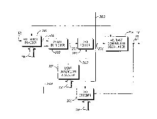
The structure and operation of the PLL frequency
synthesizer 300 is generally .qimil~r to the conventional PLL
frequency synthe,qi7:er 108 or 109 of FIG. 2, except for the addition
of a loop bandwidth adjuster 301 and a control signal at line 303.
The loop bandwidth adjuster 301 is programmed with information
at the data bus 118 and produces a loop bandwidth adjust signal at
line 302 which modifies the loop filter 203 to produce a change in
the loop bandwidth of the PLL frequency synt,heql7.er 300. The
control signal at line 303 is used to control reference divider 201,
loop divider 205, and voltage controlled oscillator 204 permitting
discontinuous operation of the PLL frequency synthesi7.er 300.
FIG. 3 illustrates only one of many alternative
interconnections, as is known in the art, which can be made
between the loop bandwidth adjuster 301 and the PLL frequency
~5 syntheqi~er 300 to control the loop bandwidth. The loop bandwidth
adjuster 301 may alternatively be coupled, for ex~mple, to the
phase detector 202 and the VCO 204, to adjust the loop bandwidth
in accordance with well known design techniques. FIG. 3 also
illustrates only one of many alternative ways, as is known in the
art, in which the blocks of the PLL frequency syntheqi7er 300 may
be coupled to the control signal at line 303 to provide for
discontinuous operation. The control signal at line 303 may
alternatively be coupled, for ex~m~lç, to the phase detector 202 and
loop bandwidth adjuster 301. Alternatively, the control signal at
line 303 may be coupled to only one elernent. of the PLL frequency
syntheqi7.er 300, for ~x~mple, the loop divider 205.
The PLL frequency synth~si~er 300 may be ~l~qsified as
belonging to one of at least two categories based on the
predetermined frequency relationship of the output signal
frequency at line 116 or 117 to the frequency of the reference
frequency signal at line 115. The first category is cl~qqified as an
"integer division" PLL frequency synthesizer wherein the
relationship between the output frequency signal at line 116 or 117
and reference frequency signal at line 115 is an integer. The
second category is cl~.~qified as a "fractional division" PLL
frequency synthe,qi~çr in which the relationship between the
output frequency signal at line 116 or 117 and reference frequency
WO 95/13666 PCT/US94111469
21~280~
g
signal at line 116 is a r~tio~l, non-integer number, consisting of
an integer and a fraction.
PLL frequency synthesi7.ers are characterized by a
resolution. The resolution of the PLL frequency syntheqi7er 300 is
- 5 defined as the minimum allowable change, or step, in thefrequency of the output signal 116 or 117. The resolution of an
integer division PLL frequency synthe,qi7.~r may be equal to, but is
no sm~ller than, the frequency of the divided reference frequency
signal 206. The resolution of a fractional division PLL frequency
synthesizer may be equal to, but is no sm~ller than, a quotient,
whose numerator is the frequency of the divided reference
frequency signal 206 and whose rlenomin~tor is the denomin~tor
of the fractional part of the value of loop divider 205. The
frequency and level of spurious sideband qign~l.q on the output
signal 116 or 117 are generally directly related to the resolution of
the PLL frequency synth~qi7.er 108 or 109.
The resolution of an integer division ;mplçm~ntation of the
PLL frequency synthç.qi7.er 300 can be adjusted by ~h~nging the
values of the lefe, ellce divider 201 and the loop divider 206 by
reprogr~mming them via data bus 118. Decreasing the value of
both dividers decreases the resolution of the PLL frequency
syntheqi7.er 300 and increasing the value of both dividers
increases the resolution.
In the ~lefeI-.ed embo~liment, fractional division is used in
the implementation of the PLL frequency syn~hçæi7çr 300. The
resolution of the fractional division implemçIlt~tion of the PLL
frequency syntheqi7er 300 can be adjusted by ~h~n~ing the value of
the denomin~tor of the fr~ctio~l part of the value of loop divider
206. Decreasing the ~ler1omin~tor via data bus 118 decreases the
resolution of the fractional division implementation of PLL
frequency synthesizer 300 and increasing the ~lenomin~tor
increases the resolution.
In the ~lefel . ed embodiment, the transceiver 100 is a
cellular radiotelephone operating in a radio frequency band
36 allocated for a particular type of cellular service. In the preferred
embodiment, the radio frequency band is used by a typical cellular
system, for ~ mple, a Narrow Advanced Mobile Phone System
WO 95/13666 PCT/US94111469
21~2~0~ _
- 10-
(NAMPS). In the NAMPS ~y~e~l, the subscriber unit Tx
çh~nn~l~ extend from appro~im~tely 824 to 849 MHz and the
subscriber unit Rx r.h~nnel~ extend from approximately 869 to
894 MHz. A portion of these Rx çh~nnel.~ from 879.39 to
880.62 MHz is allocated for control rh~nn~l~ with 30 kHz wide
rh~nnel spacing. The r.h~nnel spacing is defined as a difference
in frequency between two adjacent ch~nnel.~ of the radio frequency
band. The rem~inrler of the ch~nnel.~ in the NAMPS radio
frequency band are allocated for voice r.h~nnel~ with 10 kHz
narrow çh~nnel spacing. Theliafore, the rh~nnel spacing varies
from 30 kHz to 10 kHz over the NAMPS radio frequency band.
A further example of a radio frequency band having a
different ch~nnel spacing which may be implemented with the
present inven~ion is the Group Special Mobile (GSM) cellular
~5 system. In the GSM ~y~lem, the subscriber unit Tx ch~nnels
extend from a~vx;..~tely 890 to 915 MHz and the subscriber unit
Rx r.h~nn~l~ extend from a~.oxilll~tely 93~ to 960 MHz. The
GSM ~h~nnel spacing is 200 kHz. The present invention may be
used with a transceiver 100 r~p~hle of operating in multiple
systems. Thelarola, the r.h~nnel spacing can even vary between
the radio frequency bands of each system, for example, between
GSM and NAMPS.
According to the ~. afer led embodiment of the present
invent.ioI~, the step of determining the r.h~nnel spacing in a
2~ portion of the radio frequency band including the radio frequency
rh~nnel is performed by the processor 110. For the transceiver 100
operating in the NAMPS cell~ r system, if the radio frequency
çh~nnel to which the transceiver 100 was tuned was in the portion
of the band, 879.39 to 880.62 MHz, co~t.~ining the control rh~nnel~,
the determined r.h~nn~l spacing would be 30 kHz. If the radio
frequency ch~nnel to which the transceiver 100 was tuned was in
the rP.m~ining portion of the band cont~ining the voice c.h~nnel~,
the determined ~h~nn~l spacing would be 10 kHz.
According to the present invent.ion, the step of determining
3~ the ch~nne~ spacing in a portion of the radio frequency band
incllllling the radio frequency ch~nnel is used because it indicates
what the PLL frequency synt.hesi7.er requirements are in the
~ WO95/13666 21 S 2 8 0 9 PCT~S94/11469
- 11-
particular portiQn of the radio frequency band in the particular
system in which the transceiver is operating.
Acco. dillg to the ~lefe~-. ed embodiment of the present
invention, the step of controlling the PLL frequency synt.hesi7.er
responsive to the determined ~.h~nnel spacing is performed by the
processor 110. The determinAtion can be made simply by going to
a lookup table or alternately through a calculation or by
monitoring data on the radio frequency ~.h~nnel
An advantage of controlling the PLL frequency synt.he.ci~er
0 300 responsive to the determined ch~nnel spacing is that the
performance of the PLL frequency synthesi7.er 300iS controlled
according to the configuration of the radio system, and more
particularly the radio frequency ch~nnel to which the transceiver
100 is tuned. The result is an im~ lent in performance of the
PLL frequency syntheEi7.çr 300 over the performance that would be
realized if the PLL frequency synthesi7.er 300 were not controlled
responsive to the determined ch~nnel spacing
FIG. 4 illustrates a flowchart describing steps for operating
the novel phase locked loop frequency synt.hesi7:er of FIG. 3 in
continuous or discontinuous modes in accordance with the
present invention. The flowchart starts at step 401. At step 403
the transceiver 100 determines the r.h~nnel spacing of the radio
frequency ~.h~nnel.~ in a portion of the radio frequency band
including the radio frequency ~h~nnel. At step 402, the processor
110 controls the PLL frequency synt.hesi7:er responsive to the
determined ch~nnel spacing. When the ~h~nnel spacing is
determined to be wide at step 403, the PLL frequency synt.hesi7er
300 is operated in a discontinuous mode at step 404; the resolution
of the PLL frequency synthesi~er 300iS adjusted to be wide at step
405; and the loop bandwidth ofthe PLL frequency synt.hesi~er 300
is adjusted to be wide at step 406. When the ~h~nnel spacing is
determined to be narrow at step 403, the PLL frequency
synt.hesi7:er 300iS operated in a cont.inllous mode at step 407; the
resolution of the PLL frequency synthe~i~er 300iS adjusted to be
narrow at step 408; and the loop bandwidth of the PLL frequency
synthesi~r 300 is adjusted to be narrow at step 409.
W O 95/13666 2 1 5 2 8 ~ 9 PC~rrUS94/11469
- 1
- 12-
According to the present invent.iQn, the step 403 of
determining the ~h~nne~ spacing to be narrow, for example
10 kHz rather than 30 kHz in a NAMPS cellular ~y~lem, in(lic~tes
that the transceiver 100 is tuned to a voice r.h~nnel The PLL
frequency synt.hesi7:er 300 is advantageously operated in a
continuous mode and has the required resolution for transceiver
100 to be operated on any of the voice ch~nnel.c within the NAMPS
radio frequency band.
According to the present invention, if the rh~nnel spacing
is determined to be wide at step 403, the PLL frequency synt.he~i~er
300 can advantageously be operated in the discontinuous mode, at
step 404, to extend battery life. Through the steps of adjusting the
resolution to be wide, at step 405, and adjusting the loop
bandwidth to be wide, at step 406, the lock time of the PLL
L6 frequency synt.he.qi7:er 108 or 109 can advantageously be shortened
and the results are an even greater e~tenqion in battery life.
The advantages of the present invention are made clearer
by comparing the conventional PLL frequency sy-nt.he.si7.er 108 or
109 that is not controlled responsive to the radio frequency th~nnel
spacing in a NAMPS cellular ~y~lem. The conventional PLL
frequency synt.heqi~er 108 or 109 would be perm~nently set to have
a resolution of either 10 kHz or 30 kHz. If the resolution of the
conventional PLL frequency synt.hesi7.er 108 or 109 were set to be
10 kHz, the lock time on the control ~.h~nnel.q would be slow due to
the narrow loop bandwidth required for acceptable spurious
sideband levels in the output frequency signal 116 or 117. Data
would be lost by a convention~l transceiver 100 ~tt~mpting to
operate in the discontinuous Rx (DRX) mode. If operation in the
DRX mode were foregone, the battery life of the conventional
transceiver 100 would be shortened. Alternatively, if the
resolution of the conventional PLL frequency synt.he.si7.er 108 or
109 were set to be 30 kHz, the conventional transceiver 100 could
only tune to every third voice rh~nnel because of the restriction
caused by wide resolution and the conventional transceiver 100
would not operate in the NAMPS cellular ~y~elll.
In contrast to the prior art, the novel PLL frequency
synthesizer 300 has a wide bandwidth and wide resolution on the
~ W O 95/13666 21 5 2 8 ~ 9 PCTnUS94/11469
- 13 -
NAMPS control ~ h~nnel~ for extended battery life from the use of
the DRX mode. The novel PLL frequency synthesi~er 300
advantageously has a narrow bandwidth and narrow resolution
on the NAMPS voice ~h~nn~l~ so that transceiver 100 can tune to
every voice ch~nnel Thus the recent addition of the narrower
ch~nnel spacing of NAMPS voice rh~nnel.s, 10 kHz versus the
30 kHz spacing of the older Advanced Mobile Phone System
(AMPS), has resulted in a need for the im~love",ent~ which
result from controlling the PLL frequency synthesizer 300 in
response to the radio frequency ch~nnel spacing.
FIG. 6 illustrates a flowchart describing steps for
controlling the resolution and bandwidth of the novel phase locked
loop frequency synthesizer of FIG. 3 in accordance with the
present invention. The flowchart starts at step 501. At step 502,
the transceiver 100 determines the ~h~nnel spacing of the radio
frequency ch~nnel~ in a portion of the radio frequency band
including the radio frequency rh~nn~l At step 503, the
transceiver 100 adjusts the resolution of the PLL frequency
synthesizer 300 responsive to the determined ~h~nnel spacing. At
step 504, the transceiver 100 adjusts the loop bandwidth of the PLL
frequency synthesizer 300 responsive to the determined ch~nnel
spaclng.
In contrast to the prior art, the PLL frequency synthesizer
300 can be used in a multi-mode transceiver 100 that can operate
in either the GSM cellular system or the NAMPS cellular system,
even though the ch~nne~ spacings and lock time requirements are
vastly different. This new requirement for a transceiver 100
capable of multi-mode functionality is advantageously realized by
controlling the PLL frequency synthesi7:er 300 in response to the
radio frequency ~h~nnel spacing.
FIG. 6 illustrates a graph depicting a relationship between
the spurious sideband level, lock time, loop bandwidth, and
resolution in the novel phase locked loop frequency synthesizer of
FIG. 3 in accordance with the present invention. FIG. 6
illustrates the advantage in terms of lock time resulting from a
change in the resolution and loop bandwidth of the PLL frequency
synthesizer 300 in FIG. 3.
W095/13666 2~ j2~9 PCT/US94/11469
- 14-
The leftmost Y-axis in FIG. 6 represents lock time and is
labeled with lock times T1 and T2. The rightmost Y-axis
represents loop bandwidth and is labeled with loop bandwidths
BW2 and BW1. Lock time in a the PLL frequency synt.hesi7.er 300
is inversely proportional to loop bandwidth, the~ erole line 604 is
drawn between loop bandwidth BW2 and the corresponding lock
time T2. ~imil~rly, line 605 is drawn between loop bandwidth
BW1 and the corresponding lock time T1. The X-axis represents
the spurious sideband level at the output 116 or 117 of PLL
frequency synthesi7er 300 in units of decibels relative to the
carrier level (dBc).
Curve 601 in FIG. 6 represents a narrow PLL resolution
and gives an appro~im~te relationship between the spurious
sideband level at the output of PLL frequency synthe~ er 108 or
~5 109 and the loop bandwidth. Curve 602 represents a wide PLL
resolution and gives an appro~im~te relationship between the
spurious sideband level at the output 116 or 117 of PLL frequency
syntheci~er 300 and the loop bandwidth. Curve 601 and line 604
intersect at point 606. Curve 602 and line 605 intersect at point 607.
Line 603 is drawn between the intersection point 606 and the
intersection point 607 and intersects the X-axis at a spurious
sideband level of -S dBc. The spurious sideband level of -S dBc
represents the transceiver spurious requirements as dictated by
the system specifications or requirements, for example, of
alternate ~h~nnel selectivity. Therefore, lock time T2 is the best
that can be achieved using a narrow resolution for the spurious
sideband level -S dBc. The improved lock time T1 can be achieved,
at no degradation in spurious sidebands from -S dBc, by
controlling the PLL frequency synthesizer 300 in such a m~nn~r
so as to produce a wide resolution and increased loop bandwidth
BW1 based on a determination of a wide ch~nnel spacing on the
radio frequency chz~nnel.
21~2~09
W O 95/13666 - PCT~US94/11469
- 15 -
Thus, the present invention provides an apparatus and
method for operating a phase locked loop frequency syn~.hesi7:er
responsive to radio frequency ~.h~nnel spacing. The present
invention advantageously provides faster lock time and lower
5 noise from the PLL frequency synthesi~çr 300. This advantage
and others are generally provided by an apparatus and method
performing the steps of determining the ~h~nnel spacing of the
radio frequency ~h~nn~l~ in a portion of the radio frequency band
including the radio frequency ~h~nnel, and controlling the PLL
10 frequency synthesizer 300 responsive to the determined ch~nnel
spacing. With the present invention the prior art problems of
generating noise and spurious sidebands and mi.~ing
information due to the slow lock time of a PLL frequency
synthesizer are subst~nt.i~lly resolved.
~5 While the present invention has been described with
reference to illu~Llative embodiments thereof, it is not inte~(led
that the invention be limited to these specific embodiments. Those
skilled in the art will recognize that variations and modifications
can be made without departing from the spirit and scope of the
20 invention as set forth in the appended claims.
VVhat is claimed is: