Note: Descriptions are shown in the official language in which they were submitted.
wo 94/17619 215 2 9 01 PCT/CA93/00283
METHOD OF PROVIDING D.C. FEED TO A TELEPHONE LINE
Technical Field and Tndllctn~l Applicability
This invention relates to a method of providing d.c. feed from a line interface
circuit to a two-wire telephone line.
Back~round Art
As is well known, d.c. feed is one of a variety of functions which must be
pe,rolllled by a line interf~e circuit provided at a telephone central office (CO) or remote
terminal, and includes the supply of a direct current, generally referred to as loop current,
to a telephone line for purposes such as del~ ",il~ir~g the hook state and dial pulsing of a
telephone connected to the line and supplying a bias current or power to the telephone.
It is common to provide this current from the CO battery supply via balanced feed
resistors. Because the line impedance may vary significantly for lines of different lengths,
and because the battery voltage is relatively constant, the loop current also can vary widely
and, in particular, can be much higher for short lines than is required for proper operation
of the telephone equipment. This results in the disadvantages of undesirably high power
consumption and dissipation, especially in the feed resistors.
Although constant current d.c. feed arrangements have been proposed in order to
avoid these disadv~nt~gçs, these give rise to other disadv~nt~ges Accordingly, a need
has remained for a voltage driven d.c. feed arrangement in which the above disadvantages
are reduced.
This need is addressed in Treiber United States Patent No. 4,254,305 issued
March 3, 1981 and entitled "Current T imited Subscriber Line Feed Circuit", in which loop
current on a telephone line is sensed and used to control a voltage generator, whose output
is coupled to the line via the feed resistors, in order to reduce the supply voltage when the
loop current exceeds a threshold level of 40 mA. In this circuit, voice signals are coupled
to and from the line via a conventional transformer and electronic hybrid circuit.
With evolution of telephone line interf~re circuits, it has been recognized that it is
desirable to reduce size, cost, and power consumption, and to increase versatility, as
much as possible. This involves elimin~ting buL~y conventional transformers, using
common line drive cil-;uiLIy for d.c. feed and a.c. signal h~ntlling, and programming
components such as digital signal processors and control circui~y to enable a single line
interface circuit to be adaptable to many dirrelcllt telephone line characteristics and
telephone service c~pahilities. With such evolution, the line feed circuit arrangement of
the Treiber patent discussed above is not practical.
In Chea, Jr. United States Patent No. 4,315,106 issued February 9, 1982 and
entitled "Apparatus For Regulating Current Supplied To A Telephone Line Signal Of The
Type Employed In Digital Telephone Systems" there is described an arrangement in which
loop current is regulated by a differential amplifier and ~ ing arrangement whose
Wo 94/17619 PCT/CA93/00283
'~`5~529~1
output is used to control a voltage amplifier, which may be constituted by a d.c. to d.c.
converter, to produce a supply voltage for the line. This patent does not address the
coupling of signals to and from the line.
In the related Chea, Jr. United States Patent No. 4,317,963 issued March 2, 1982and entitled "Subscriber Line Tnt~rfare Circuit Utilizing Irnpedance Synthesi7~r And
Shared Voltage Source For Loop Current Regulation Control" the supply voltage isdescribed as being switched among a plurality of voltage sources for loop current
regulation, and signals are coupled to the line via amplifiers which with their surrounding
components are described as comprising "a pair of buffer amplifiers capable of h~n~lling
the dc and ac electrical re4uhG~ ,nts of the SLIC function". There is no further description as to the extent of these requirements or how they would be met.
There are many such r~uuc;"~ents of the line interf~e circuit function which arewell known in the art, and which are both stringent and difficult to meet in a versatile and
adaptable manner. One of these re~luu~mel,~. is to permit reversal of the polarity of the
supply voltage to the telephone line. Generally, this re4ui,~"lent has been met by
providing a polarity reversing relay via which the line intçrf~ce circuitry is coupled to the
line, but the reversing relay is a mech~nical Colll~)ollenl of the line int~.rf~ce circuit,
constituting part of its bulk and cost and being subject to mechanical failure. It is
accordingly desirable to avoid the need for this reversing relay while still meeting the line
intçrf~e circuit ,~qu,~ lents. However, the latter Chea, Jr. patent would require that a
reversing relay be present to perrnit polarity reversal.
In Bolus et al. United States Patent No. 4,431,868 issued February 14, 1984 and
entitled "Solid State Telephone Line Tntçrf~e Circuit With Ringing Capability" there is
described a line intçrf~ce circuit in which both d c. and a.c. signals are supplied to the
inputs of high-voltage tip and ring wire amplifiers whose outputs are coupled to the line.
The d.c. levels at the amplifier outputs are d~ t~ - " ,il~ed by d.c. potentials at the amplifier
inputs and the d.c. gain of the arnplifiers. The description states that it is possible for the
tip and ring d.c. polarities to be reversed by reversing the polarities at the inputs to the
amplifiers, but does not discuss this further.
This patent is concerned with using the ~mplifiçrs also to produce a (high voltage)
ringing signal waveform on the line, as well as to couple voice signals to the line. To
these ends, and to ensure operation of the arnplifiers within linear parts of their
characteristics, the supply voltage rails of the arnplifiers are controlled to follow, with an
offset, the instantaneous values of the ringing signal waveform or d.c. feed characteristics
which are not described in detail. The supply voltage rails are coupled to outputs of a d.c.
to d.c. converter which is controlled by a sensing circuit and error amplifier in dependence
upon the supply voltages and the amplifier output voltages.
wo 94/17619 21 ~2 9 o i PCT/CA93,002~.3
In the Bolus et al. patent the two amplifiers must be operated in a high-gain
configuration, thus requiring that the gain-bandwidth product of the amplifiers be much
larger than the bandwidth required to support telephony signals. In addition, the
amplifiers must accommodate the high ringing voltages, and therefore must be fabricated
S using a very high voltage silicon process. This combination of ~uilwllellts makes the
approach of the Bolus et al. patent impractical. To carry a variety of voice and data traffic,
including ISDN signals, requires an even larger bandwidth, and also adds a requirement
for a fast slew rate. The approach of the Bolus et al. patent is also il~pl~c~ical for meeting
these additional re~lui~~ nts.
An object of this invention is to provide an improved method of providing d.c.
feed to a two-wire telephone line.
Disclosure of the Invention
According to one aspect of this invention there is provided a method of providing
d.c. feed to a two-wire telephone line, comprising the steps of: generating a supply
15 voltage for a drive circuit including two amplifiers each having an output coupled to a
respective wire of the line, the drive circuit serving to supply a tran~mi~sion (e.g. voice)
signal to the line via the amplifiers; ~el~ i ng potentials at the amplifier outputs in
dependence upon the supply voltage and headroom voltages required for operation of the
amplifiers to supply the tran~mission signal to the line, a difference ~tweell the potentials
20 at the outputs of the two amplifiers producing a loop current on the line; and monitoring
the loop current on the line; characterized by controlling the generated supply voltage in
dependence upon the moni~ol~d loop current by the steps of: producing a target value
corresponding to a target voltage inversely dependent upon an amount by which the
moni~oled loop current exGeeds a prede~ ed value; and adjusting the genel~t~;d supply
25 voltage towards the target voltage in depentl.once upon the target value; and iteratively
lGI~eaLillg these steps whereby the target voltage and the gen~,ld~d supply voltage
converge.
As the generated supply voltage d~termines the amplifier output potentials
producing the loop current on the line, and is controlled in dependence upon the30 mol~itol~d loop current, this arrangement serves to limit the loop current in a desirable and
controlled manner, while maint~ining desired headrooms for the amplifiers so that they
can accommodate signals for supply to the line without distortion or clipping.
A convenient prerletermined value of the monitored loop current is about 20 mA,
this being the Il~ihlilllulll current required for proper operation of some telephones which
35 may be connected to the line. Thus the more the monitored loop current exceeds this
predetermined value, the smaller can be the magnitllde of the target voltage, to produce an
initially bigger dirr~ ce between the genel~ted supply voltage and the target voltage.
wO 94/17619 2 1 5 2 9 b 1 PCT/CA93/00283
It is advantageous if the step of adjusting the generated supply voltage is iteratively
repeated at a faster rate for large dirrGlc,lces than for small differences between the
~encldlGd supply voltage and the target voltage. The different rates enable particularly
high loop currents, which may be due to a very short telephone line or due to a fault such
5 as a short-circuit of the line, to be reduced rapidly, while providing for stable operation in
conjunction with dirr~lclll types of telephone connected to the telephone line.
For example, the step of adjusting the genGld~ed supply voltage can be iteratively
e~ealed at a rate of at least about once per millisecond for large differences, and at a rate
of at most about once per 10 milliseconds for small differences, between the target voltage
10 and the generated supply voltage. In an embo-lim.-nt of the invention described below,
adjuctm~nt.c are effected every 0.5 ms and every 100 ms for respectively large and small
differences between the supply voltage and the target voltage. These rates and times are
given by way of example of typical p~u~llelGl~ which may be selected in particular
cil~ullls~lces, and other values may be chosen.
In order to provide a well-controlled convergence of the generated supply voltage
and the target voltage, which l~A;11~ C stable operation for various types of telephone
connected to lines with various characteristics, each adjllctment of the geneldted supply
voltage towards the target voltage can be by an amount which is a pre~let~rminecl fraction,
for example one sLb~Gell~h, of a difference bGlweGIl the gGIleldlGd supply voltage and the
20 target voltage.
Preferably, as in an embodiment of the invention described in detail below, the
two amplifiers are d.c. amplifiers and the step of det~ i ng potentials at the amplifier
outputs comprises: coupling the generated supply voltage between two supply lines of the
drive circuit whereby the supply lines have relative potentials of zero volts and the
25 generated supply voltage; for a first one of the amplifiers whose output is coupled to a tip
wire of the line, de~llllining a potential at an input of the amplifier by passing a controlled
current through a resistance, to produce at the output of the amplifier a tip potential which
is offset from zero volts, towards the generated supply voltage, by a tip headroom
voltage; and for a second one of the amplifiers whose output is coupled to a ring wire of
30 the line, determining a potential at an input of the amplifier by passing a controlled current
through a resist~nre, to produce at the output of the amplifier a ring potential which is
offset from the generated supply voltage, towards zero volts, by a ring headroom voltage.
This method conveniently further comprises the step of selectively reversing
polarity of d.c. feed to the line by increasing the controlled ~;Ull~,llt~ SO that each of the tip
35 and ring headroom voltages exceeds half the generated supply voltage. Typically in this
case the tip and ring headroom voltages are set to approach, but not reach, the generated
supply voltage to provide a maximum reversed polarity d.c. feed to the line while still
operating the amplifiers within a linear part of their characteristics, to ensure linear
wO 94/17619 21 S29~ PCT/CA93/00283
amplification without signal distortion or clipping. The tip and ring headroom voltages
can be adjusted in conjunction with the generated supply voltage in the reversed polarity
state, to m~int~in the desired linear operation of the amplifiers while limiting the loop
current on the line.
Thus the invention enables the loop current on the line provided by the two drive
amplifiers, via which the tr~n~mi~ion signal is coupled to the line, to be limited in a
manner which ~ sufficient headroom between the drive amplifier outputs and the
supply rails to ensure adequate linearity for the tr~n~mi~sion function. The drive
amplifiers are conveniently unity-gain buffers for maximum bandwidth and stability.
According to another aspect this invention provides a method of providing a
controlled loop current with selectively reversible polarity on a two-wire telephone line,
comprising the steps of: supplying to two ~mplifi~rs, each having an output coupled to a
respective wire of the line, supply potentials differing by a supply voltage; determining a
potential at the output of each amplifier to be offset by a respective headroom voltage from
a re~e~;Li~e one of the supply potentials towards the respective other supply potential, a
difference between the potentials at the amplifier outputs producing a loop current on the
line; selectively increasing the headroom voltages each to exceed half the supply voltage to
reverse the polarity of the loop current; monitoring the loop current; iteratively adjusting
the supply voltage towards a target voltage which depends on the loop current, thereby to
control the loop current; and if the polarity of the loop current is reversed, adjusting the
headroom voltages in dependence upon the supply voltage.
As already indicated, the step of iteratively adjusting the supply voltage towards
the target voltage preferably comprises changing the supply voltage more rapidly for large
differences than for small differences bc~ween the supply voltage and the target voltage.
According to a further aspect this invention provides a method of controlling loop
current on a two-wire telephone line, the loop current being produced by a difference
between potentials at outputs of two amplifiers for coupling a tr~nsmis~ion signal to the
line, said potentials being offset towards one another from supply potentials of the
amplifiers by respective amplifier headroom voltages for accoln,l,odating the tr~nsmi~ion
signal, the supply potentials differing by a supply voltage, comprising the steps of:
monitoring the loop current on the line; and iteratively adjusting the supply voltage,
towards a target voltage which depends on the monitored loop current, at a faster rate for
large differences than for small differences between the supply voltage and the target
voltage.
Brief Description of the Drawin~s
The invention will be further understood from the following description with
reference to the accompanying drawings, in which:
WO 94117619 ~ 52~3 PCT/CA93/00283
~; 6
Fig. 1 is a block diagram illustrating a telephone line interface circuit which
operates in accordance with the method of this invention; and
Figs. 2 and 3 are voltage-time diagrams, and
Figs. 4, 5, and 6 are flow charts, with reference to which operations of the line
interface circuit of Fig. 1 in accordance with the method of this invention are explained.
Mode(s) of Carrying Out the Invention
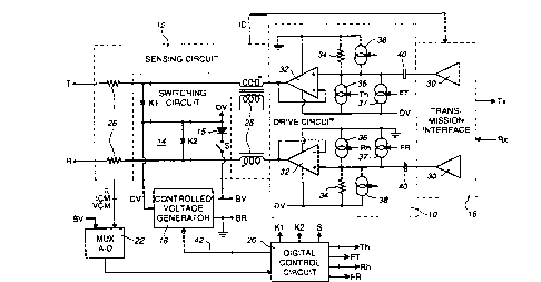
Referring to Fig. 1, there is illustrated a block diagram showing parts of a
telephone line interf~e circuit, which is assurned in the following description to form part
of and be located at a telephone central office (not shown), or CO, but which may
~ltern~tively form part of a remote terrnin~l which is coupled to a CO via a multiplexed
co~.""~ ications path. Only those parts of the line i~lt~r~ce circuit which are relevant to a
full underst~nrling of this invention are shown in Fig. 1.
As shown within broken outlines, the line interface circuit comprises a drive
circuit 10 which is coupled to terminals T and R, for connection to the tip and ring wires
of a two-wire telephone line, via a sensing circuit 12 and a ~wilching circuit 14. The drive
circuit 10 is also coupled to a tr~ncmiC.cion int~ ce 16 which co."",~ icates with the
rem~in-ler of the CO via Ll~ls~ and receive signal paths Tx and Rx respectively. The
line interface circuit also includes a controlled voltage generator 18, a digital control circuit
20, and a multiplexing analog-to-digital (A-D) converter 22.
The drive circuit 10, sensing circuit 12, and tr~ncmiscion interface 16 are
conveniently of the form fully described in Tntern~tional patent applications No. 92/00135
filed April 3, 1992 and entitled "Telephone Line Circuit With Voltage Switching" and
No. 93/00105 filed March 17, 1993 and entitled 'Yelephone Line Circuit With Voltage
Control". The drive circuit 10 is also described below. Only those parts of the sensing
circuit 12 and the tr~ncmiccion interface 16 which are essen~i~l to a full understanding of
this invention are illustrated in Fig. 1 and are described below.
The sensing circuit 12 includes a b~l~nced arrangement of feed resistors 26
connected in series with windings of a small a.c. sensing transformer 28 between the
outputs of the drive circuit 10 and the terminals T and R, and produces output signals ID,
IL, ICM, and VCM. The signal ID represents the di~ltlltial a.c. or signal current on the
telephone line and hence flowing via the terminals T and R, and is supplied to the
tr~ncmicsion interface 16. The signal IL represents the loop current on the telephone line,
i.e. direct current flowing in opposite directions via the two t~rmin~lc T and R, and the
signal ICM represents the comrnon mode current on the telephone line, i.e. current
flowing in the sarne direction via the two t~nnin~lc T and R. Individual currents on the tip
and ring wires of the telephone line are l~s~ecLively the sum and difference of the common
mode current and the loop current. The signal VCM represents a common mode voltage
wo 94/17619 1 S29 o~ PCr/CA93/00283
on the telephone line when the feed resistors 26 are disconnected from the terminals T and
R by the opening of contacts, not shown, of a protection relay.
The tr~n~mi~sion interfaçe 16 produces a signal on the transmit path Tx from the- differential current signal ID, and includes amplifiers 30 having low ilnpedance outputs,
5 constit~lt~ng outputs of the tr~n~mi~iQn interface 16 coupled to the drive circuit 10, at
which are produced complt;lllellt~y signals derived from a signal received via the receive
path Rx.
The drive circuit 10 comprises two circuits, associated with the tip and ring
tçrmin~l~ T and R respectively, each of which comprises a d.c. buffer amplifier 32, a
10 resistor 34, a controlled current source 36, two switched current sources 37 and 38, and a
coupling capacitor 40. Each amplifier 32 has its output, constitl~ting a respective output of
the drive circuit 10, connected to its inverting input to provide the amplifier with a unity
gain so that these amplifiers have a ma~illlulll bandwidth and a .~,i.~i...l".~ output
im~nce. Each amplifler 32 has its non-inverting input connected via the capacitor 40 to
15 a respective output of the tr~n~mi~ion int~rf~ce 16, via the resistor 34 in parallel with the
switched current source 38 to a first voltage supply rail (ground or æro volts for the tip
side because in normal d.c. feed the tip wire is held at a voltage close to ground, and at a
drive circuit supply voltage DV for the ring side because in normal d c. feed the ring wire
is held at a voltage close to this voltage DV, as described further 'Delow), and via the
20 controlled current source 36 in parallel with the switched current source 37 to a second
voltage supply rail (DV for the tip side, and ground for the ring side). The amplifiers 32
are supplied with power from the ground and DV voltage supply rails.
Currents passed by the controlled current sources 36 are precisely controlled byeight-bit digital signals supplied by the digital control circuit 20; these signals and their
25 decimal values are referred to as Th and Rh (for Tip headroom and Ring headroom
respectively). Currents passed by the current sources 37 are switched on or off by binary
signals FT and FR supplied by the digital control circuit 20. The switched current sources
38 are turned on, by control circuitry (not shown) within the drive circuit 10, when the
currents passed by the current sources 36 are at a very low value and the current sources
30 37 are switched off, as is further described below. As an ~ltern~tive which is not further
described here, the switched current sources 38 could be controlled directly by binary
signals supplied by the digital control circuit 20.
The switching circuit 14 comprises two latching relays, referenced Kl and K2,
and an electronic switch S which are controlled by correspondingly referenced control
35 signals supplied by the digital control circuit 20. The relays are shown in a reset state
having one open contact (represented by an X) and two closed contacts (each represented
by a vertical bar), one of which is in the path from the output of a ,~s~e.;~ive amplifier 32
to the respective terminal T or R, and the other of which is in a series path from an output
wo 94/17619 21~ 2 9 0 1 PCT/CA93/00283
of the controlled voltage generator 18 to the drive circuit supply voltage line DV. In this
state the switch S, which is in series between a -48 volt battery voltage line BV and the
drive circuit supply voltage line DV, is open, and the controlled voltage generator 18 is
controlled by the digital control circuit 20 via a path 42 to g~,nelat~ a controlled voltage CV
5 which conctit-ltes the drive circuit supply voltage DV. A grounded battery return line BR
is also connected to the controlled voltage generator 18. The ~.wilching circuit 14 also
includes a diode 15 connected in series with the switch S, which diode serves to prevent
contention between the voltages CV and BV during opening (turn-off~ of the electronic
switch S.
In another operating state, which is used to conserve power in the on-hook or idle
state, the digital control circuit 20 renders the controlled voltage generator 18 inactive, so
that its output presents a high impeA~nce, and closes the switch S so that the battery
voltage BV constitutes the drive circuit supply voltage DV. Other operating states of the
switching circuit 14 and the controlled voltage generator 18, not relevant to the d.c. feed
15 of this invention, and further details of these parts of the line interface circuit, are fully
described in International patent application No. 92/00135 and United States Patent No.
5,103,387 issued April 7, 1992.
The signals IL, ICM, and VCM produced by the sensing circuit 12 are supplied to
inputs of the multiplexing A-D converter 22, whose digital outputs are supplied to the
20 digital control circuit 20. The battery voltage BV is also supplied to an input of the
converter 22 so that this voltage can be monitored by the digital control circuit 20. The
digital control circuit 20 monitors the rligiti7~1 signals IL, ICM, VCM, and BV and
operates in accordance with a stored prograrn, for example down-loaded from the CO, to
produce the various control signals discussed above and thereby to dete- "~ e ap~l~liate
25 operating conditions for the re~ind~r of the line interface circuit. Such up~ g
conditions include that of d.c. feed in both normal and ~ ed polarity states as further
described below.
By way of example and not limit~tion, in the following description it is assumedthat the battery voltage BV is derived from a telephone CO battery and is typically a little
30 more negative than -49 volts, but may fall below (i.e. be more positive than this) when the
battery is relatively discharged, and that the battery return termin~l BR is at 0 volts. The
controlled voltage generator 18, when enabled and supplied with a control signal Cv via
the path 42 from the digital control circuit 20, generates the controlled voltage in
accordance with the e~quation:
CV = -56 + Cv * 0.182 volts.......... (l)
where Cv is an integer from 0 to 255. Thus a zero value of Cv corresponds to a
maximum controlled voltage CV of -56 volts, and a maximum value of 255 of Cv
corresponds to a minimum controlled voltage CV of about -9.6 volts.
wO 94/17619 PCT/CA93/00283
,. 2.1~,9~
It is also assumed that each resistor 34 has a resistance of 475 kQ, and that each
capacitor 40 has a capacitance of 0.1 ~LF, so that these components together provide
(when the switched current sources 37 and 38 are off) a time constant of the order of
50 ms for d.c. voltage changes at the non-inverting inputs of the amplifiers 32. Each
controlled current source 36 passes a current from 0 to 128 ~lA as clet~rmined by the
respective control signal Th or Rh, each of which is an integer having a value from 0 to
255. Thus the ~spe~;~ive tip or ring voltage dropped across the resistor 34, referred to as
a headroom voltage H, is given by the equation:
H = 0.475 * 128 * h / 255 volts...... (2)
10 where h is the decimal value of the respective control signal Th or Rh.
In order to m~int~in bias conditions in the drive circuit, the headroom signals h are
allowed by the software in the digital control circuit 20 to have a ~ ,-m digital value of
3. This corresponds to a current through the controlled current source 36 of about
1.5 ,uA, and in accordance with the above equation to a headroom voltage of less than one
volt which would not be practical. Accordingly, such a very low current situation is, as
mentioned above, lete~t~l within the drive circuit 10 and used to turn on the switched
current source 38, which passes a relatively high current for example in a range from
about 0.1 to 10 mA, e.g. 0.5 mA. This enables the m~gnit~ldes of the respective
headroom voltage H to be rapidly decreased, within a time which is much less than the
time constant defined by the resistor 34 and capacitor 40. The drive circuit 10 also
includes ~ cuilly, not shown, for bypassing the resistors 34 and providing a rapid charge
or discharge of the capacitors 40 in the event that the drive circuit supply voltage DV is
reduced quickly and the output voltages of the amplifiers 32 come too close to the supply
voltages DV and ground.
The switched current sources 37 similarly serve to permit the m~gnit~ldes of theheadroom voltages TH and RH to be rapidly increased within a time much less than the
time constant defined by the resistor 34 and the capacitor 40. For this purpose, the
current sources 37 are turned on by the binary control signals FT and FR from the digital
control circuit 20, and each source 37 is acsllm~cl to pass a current of about 450 ~LA when
it is turned on. The switched current sources 37 and 38 pass substantially no current
when they are turned off.
For the control functions described below, the digital control circuit 20 uses adigital representation of the loop current IL produced via the multiplexing A-D converter
22. As the loop current IL can flow in either direction around a telephone subscriber loop
connected to the terminals T and R (depending on the applied polarity as described further
below), the digital control circuit 20 uses a digital representation of the absolute value of
the loop current. In the following description. the designation Ilp is used to refer to an
integer which constitlltes this digital representation and can have a decimal value from 1 to
wo 94/17619 215 2 ~ ~ ~ PCT/CA93/00283
128. For convenience, the value of np corresponds directly to the loop current IL
measured in milli~mps. For example, a sensed loop current IL of _3.5 mA is represented
by an Ilp value of 4, and a sensed loop current IL of +127.5 mA or more is represented
by an Ilp value of 128.
It is observed that, in order to accommodate manufacturing tolerances and
variations in the hardware of the line interface circuit, the digital control circuit 20 can also
store various calibration values for pararneters such as the loop current, which calibration
values can be used by the digital control circuit to ensure precise operation as described
herein of the particular line interface circuit. For example, the value np representing the
loop current IL is produced accurately in the digital control circuit 20 by modifying the
actually sensed loop current in accordance with a stored loop current calibration value.
The cornmon mode current and voltage signals ICM and VCM also supplied to the
digital control circuit 20 are used for other control functions than those described here,
and accordingly are not further discussed. When the battery voltage BV is at least -49
volts and a connected telephone line is in an on-hook state, the digital control circuit 20
renders the controlled voltage gc"eldtor 18 inactive to conserve power and closes the
switch S so that the battery voltage is used to power the line. In this state the digital
control circuit 20 monitors the battery voltage BV via the A-D converter 22 every 0.5 ms.
In the event that the battery voltage BV becomes more positive than -49 volts, this is
cletect~l by the digital control circuit 20, which then activates the controlled voltage
generator 18 to generate a voltage of -56 volts to power the line even in this on-hook state.
The digital control circuit 20 uses the absolute loop current value np to distinguish
between the on-hook and off-hook states of the line, np < lo representing the on-hook
state and np, 13 representing the off-hook state. np values from 10 to 13 constitute a
dead zone, in which the previous hook state is pl.,sulncd to have been m~int~ine~l, to
avoid oscillations belwcen the dirr~ states due to loop imped~nces
The following description relates to the operation of the line interface circuit in the
off-hook state of the line, and relates to three particular ope.~ ,g conditions which are
referred to as current limiting, polarity reversal, and return to normal polarity conditions.
These condi~ions are explained with reference to voltage-time diagrams in Figs. 2 and 3
and flow charts in Figs. 4, 5, and 6.
As is well known, the resistance of a telephone line which may be connected to the
terminals T and R is dependent upon the length of the line, and in the off-hook state may
also vary in dependence upon the number of off-hook telephones connected to the line,
the total resistance varying for exarnple from about 0 to more than 1900 Q. In
conventional arrangements in which the CO battery is used as a d.c. source for the loop
current on the line, the current can be high for short telephone lines, leading to excessive
power consumption and dissipation. The current limiting condition of the line interface
wo 94/17619 21 ~29 ~1 PCT/CA93/00283
circuit of Fig. 1 operates to sense the loop current IL and to control the voltage applied to
the terminals T and R so that this current is limited in a desirable manner. At the same
time, this condition is arranged to ensure that adequate tip and ring headroom voltages
exist to permit the tr~n~mi~sion of voice signals ~lween the telephone line and the
5 tr~n~mic~ion interf~e 16 without distortion or clipping by the drive circuit 10.
It is also well known that it is desirable, for example for sign~lling purposes, to be
able to reverse the polarity of the d.c. feed to the telephone line; conventionally this is
effected by a reversing relay via which the line is connected to the terminals T and R.
With the line interface circuit of Fig. 1 such a reversing relay can be dispensed with, and
10 polarity reversal, and return to normal polarity, can be errecled by st~çnng the voltages at
the non-inverting inputs of the amplifiers 32 and hence at the terminals T and R. These
correspond to the polarity reversal and return to normal polarity conditions referred to
above and further described below. In the le~el~ed polarity condition, it is still desirable
for the current limiting condition to be applied and it is still necess~ry for adequate tip and
15 ring headroom voltages to be m~int~ined.
Referring to Fig. 2, the current limiting Op~,.d~ g condition is represented by
several voltages shown as a function of time. It should be noted that time is represented
linearly over a short period of about 4 ms to the left of a vertical dashed line in Fig. 2, and
linearly over a much longer period of 1200 ms to the right of this line. The voltages
20 shown in Fig. 2 are a zero voltage (OV), the voltage DV supplied to the drive circuit 10
and con~titutecl by the controlled voltage CV of the controlled voltage generator 18, a tip
wire voltage TV which is offset from (more negative than) OV by a constant normal tip
headroom voltage TH, a ring wire voltage RV which is offset from (more positive than)
the drive circuit voltage DV by a constant normal ring headroom voltage RH, and a target
25 voltage TG.
The outputs of the tip and ring amplifiers 32 are controlled to be at the voltages TV
and RV respectively, so that the difference TV-RV constitutes a d.c. feed voltage for the
line connected to the tenmin~l~ T and R, the resulting loop current IL which flows being
dependent upon this voltage difference and the line resistance. The tip and ring headroom
30 voltages TH and RH respectively, i.e. the voltages by which the outputs of the amplifiers
32 are offset towards one another from the supply voltages of the drive circuit 10,
accommodate the maximum amplitude a.c. voltages of tr~n~mi~sion signals (e.g. voice or
information signals) on the line and a minimllm dirrelel "al between the amplifier output
and supply voltages to accommodate tolerances and avoid distortion. By way of example,
35 these headroom voltages are selected by the headroom control signals Th and Rh both
having the value 17, so that from equation (2) the headroom voltages TH and RH are both
about 4 volts.
Wo 94/17619 215 2 9 01 12 PcrlcA93loo283
Initially on detection of an off-hook condition, as shown at the left of Fig. 2, via
the path 42 the digital control circuit 20 turns on the controlled voltage generator 18
(unless it is already on due to a discharged CO battery) and controls it by supplying the
decimal value Cv = O to generate the m~illlulll voltage of -56 volts.
The digital control circuit 20 operates cyclically, performing a variety of software
functions in respective time slots every 0.5 ms. The current limitin~g operation is one of
these software functions (other functions include, for example, calibrating the sensed loop
current and monitoring the battery voltage as discussed above, and updating a timer which
is used for timing waiting periods discussed below), and accordingly a software routine
for carrying out the current limiting operation is returned to every 0.5 ms. This routine is
represented by the flow chart in Fig. 4 and is further described below.
In a first step 401 in Fig. 4, the digital control circuit 20 calculates a desired
change for the drive circuit voltage DV, based on the sensed loop current. This
calculation includes det~ g a target decimal value Tv from the loop current value np
using the equation:
Tv = 8 * (Ilp - 21).................. (3)
with Tv having a minimllm value of 0 for Ilp < 21 and having a maximum value of 255
for Ilp 2 53, and de~ ,-;nil-g an adjustment decimal value Av using the equation:
Av = (Tv - Cv) /16 .................. (4)
20 The target value Tv has the same relationship to the target voltage TG as the value Cv has
to the controlled voltage CV as defined by equation (1). Thus TG = -56 + Tv * 0.182
volts.
It should be noted that the constants in equation (3) are given by way of example
and can be varied to suit particular circumstances. The constant 21 defines a threshold
25 loop current of 21 mA above which the current limiting operation is effective, and is
chosen to be equal to the ~in;.~...n~ required current of 20 mA plus a ma~i.llulll sensing
error of 1 mA. The factor 8 delelll~ines the steepness of the current limiting and is chosen
to optimize the power ~icsiration while still n~A;I~l~;ning a proper loop current to ensure
correct operation of the telephone, especially with telephones whose characteristics (e.g.
30 sidetone and transmit levels) are dependent upon the loop current. Both the threshold and
the steepness of the current limiting operation may thus be varied as desired.
Similarly, the constant 16 in equation (4) is given only by way of example. Thisdivision factor is selected to achieve a desired rate of convergence between the voltages
TG and CV in a stable manner and without overshoot. The result of the division is
35 truncated by the digital control circuit, with positive results becoming the next lower
positive integer and negative results becoming the next higher negative integer, to create a
dead zone which prevents hunting (e.g. when the detected loop current changes due to
wo 94/17619 01 PCT/CA93/00283
13
signal cullen~) and which is offset in favor of providing a higher current. This division
factor can be varied to control the size of the dead zone and the rate of convergence.
In a step 402 in Fig. 4, a decision is made as to whether a change is to be madeimmeAi~tely (i.e. within the 0.5 ms period) or after a waiting period delel,l~ ed by a
5 timer; this decision is discussed further below. In a subsequent step 403, a change in the
decimal value Cv is made by adding the de~ ecl adjuctn~ent value Av to it; in other
words the value Cv is replaced by Cv + Av. The value Av can be positive to reduce the
voltage DV, or it can be negative to increase the voltage DV for example in the event that
the loop resistance increases due to an extension telephone being placed on-hook. Also in
step 403, a 100 ms timer is started.
In a step 404 in Fig. 4, a status bit discussed further below is checked to
dçt~rmine whether reversed polarity is being applied to the line. If not, then as indicated
by a step 405 the normal polarity headrooms discussed above (Th = Rh = 17, so that
TH = RH = 4 volts) are used. In the case of reversed polarity being applied to the line, as
in(lic:~tçd by a step 406 dir~r~;nt headroom voltages are calculated and used; this is
discussed further below with reference to Figs. 3 and 5.
As illustrated in Fig. 2, the current limiting control is such that over time the
target voltage TG and the drive circuit voltage DV converge to approximately (to avoid
control loop oscillations) the same value. The decision made in the step 402 selects one of
two possible rates at which this convergence takes place. For relatively large differences
between the target voltage TG and the drive circuit voltage DV, and hence for relatively
large values of the adju~l,llell~ value Av (e.g. for Av > 5 in the case of normal polarity,
and for Av > 8 in the case of reversed polarity), it is d- t~- "~ eA at step 402 that there
should be no waiting period, and successive changes to the controlled voltage CV at step
403 can be made every 0.5 ms. This is represented in Fig. 2 to the left of the vertical
dashed line, where there is a rapid convergence of the voltages TG and DV over a short
period. For smaller differences and adjustment values the decision at step 402 is to wait
until expiry of the 100 ms timer started at step 403 in a previous cycle; consequently such
smaller changes to the controlled voltage CV are made only every 100 ms, as shown in
Fig. 2 to the right of the vertical dashed line.
These dirr~lent rates of change of the controlled voltage CV, and hence the drive
circuit voltage DV, provide the advantages of staWity of the control loop and no audible
noise for small changes with various dirrel~l l types of telephone connected via the line to
the terminals T and R, and rapid reduction of the drive circuit voltage in the event that the
loop current is suddenly increased, for example due to a telephone going off-hook. As
already indicated above, all of the particular p~dme~l~ used in these respects can be
varied to suit particular ci~ll",~ -ces, and it is also observed in this respect that dirr~lcl~l
timer periods can be used for the normal and reversed polarities applied to the line. By
wo 94/17619 PCT/CA93/00283
2152901 14
way of example, however, it is observed that the rapid rate of change of the controlled
voltage CV may be at least about ten times the slower rate; for example the faster rate may
involve a change every milli~econd or less, and the slower rate may involve a change
every 10 ms or more.
It is observed at this point that the target voltage TG represented in Fig. 2 is not,
and need not be, physically produced in the operation of the line interface circuit, but is
referred to for providing a full understanding of the control of the controlled voltage CV to
achieve current limiting in accordance with the invention. The target voltage TGcorresponds directly to the value Tv, which as indicated especially by equations (3) and
(4) above is involved in the d~,t~ fillation of the adju~trn~nt of the controlled voltage CV
in dependence upon the loop current value Ilp.
Fig. 3 illustrates, in a voltage-time diagram similar to that of Fig. 2 but not
showing any target voltage TG, the tip, ring, and drive circuit voltages TV, RV, and DV
respectively for the polarity reversal and return to normal polarity conditions. Polarity
reversal is effected between times tl and t3 in Fig. 3 in accordance with the flow chart in
Fig. 5. Return to normal polarity is er~;led between times t4 and t5 in Fig. 3 in
accordance with the flow chart in Fig. 6. Between the times t3 and t4 in Fig. 3 the current
limiting condition described above applies with reversed polarity.
In a first step 501 in Fig. 5, at the time tl in Fig. 3, a reversal of the polarity of the
tip and ring voltages TV and RV applied to the line via the t.orrnin~ls T and R is started by
ren~ring the controlled voltage ~eneldl~l 18 active to gcllcld~e its full voltage of -56 volts
(Cv = 0 on the path 42), unless the controlled voltage generator is already active in which
case no change is made in step 501, the generator l~l "~i ni ng active as controlled by the
prevailing value of Cv. In a step 502, a "fast reverse polarity" state is set, and as
illustrated by a wait step 503 this state is m~int~ined for a period of 16 ms, until a time t2
in Fig. 3. A shorter period than 16 ms, for example 12 ms or only 8 ms, may
alternatively be used.
In the fast reverse polarity state the digital control circuit 20 turns on the switched
current sources 37 via the binary signals FT and FR, and also sets the tip and ring
headroom control signals Th and Rh to their ,naxi---um value of 255. As a result, as
shown in Fig. 3 the tip and ring voltages TV and RV, defined by the voltages at the non-
inverting inputs of the amplifiers 32, are moved rapidly to the opposite supply voltage
rails (i.e. the tip voltage TV is moved to the voltage DV, and the ring voltage RV is moved
to OV), where they are clamped, and the current sources are turned off, until the time t2 by
the physical constraints of the drive circuit.
At the time t2 the digital control circuit 20 turns off the switched current sources
37 via the signals FT and FR and, as shown by a block 504 in Fig. 5, calculates and sets
new tip and ring headrooms for the reversed polarity state. These are maintained for a
wO 94/17619 ~s290l PCT/CA93/00283
loop settling waiting period of 100 ms between the times t2 and t3 as shown by a block
505 in Fig. 5, this period being sufficient to allow ringing or other variation of the tip and
ring voltages TV and RV (shown by dashed lines in Fig. 3 during this period) to subside
and for these voltages to settle at their values determined by the calculated reverse polarity
headrooms. As shown by a block 506 in Fig. 5, at the time t3 the digital control circuit 20
sets a polarity status bit to indicate the reversed polarity of the line, this bit being checked
at the decision block 404 as already described above, and continues with the current
limiting op~l~Ling condition represented in Fig. 4. This operating condition, represented
belween the times t3 and t4 in Fig. 3, is as already described above except that, due to the
reversed polarity decision at the block 404, for each change of the controlled voltage CV
the headrooms are recalculated as shown by the block 406.
The calculation of appropliate headrooms for the reversed polarity state as
represented in blocks 406 and 504 is described below. As shown in Fig. 3, in thereversed polarity state the headroom voltages TH and RH are relatively large, being
measured from OV to the tip voltage TV and from the drive circuit voltage DV to the ring
voltage RV respectively, and furthermore these headroom voltages must be varied with
variation of the drive circuit voltage DV. Due to the large m~gnit~lcle of the headrooms in
the reversed polarity state, in order to m~int~in linear operation of the amplifiers 32 the
headroom voltages must be clet~rminecl in a manner to take into particular account
tolerances and manufacturing variations of the line interface circuit. To facilitate. this, the
digital control circuit 20 stores a parameter Rb for the particular line int~rf~e circuit. The
p~d-l~et~l Rb represents the control signal values Th and Rh which are necessary to
provide the line interface circuit with desired headrooms on entry into the reversed polarity
state with the full controlled voltage CV. In other words, between the times t2 and t3 in
Fig. 3, when Cv = 0, Th = Rh = Rb. The value Rb is typically in a range of about 190 to
200 or more.
In an embodiment of the invention, the headroom control signal values Th and Rh
are calculated to be equal to Rb - Cv * 3 / 4 for values of Rb less than 200 and to be equal
to Rb - Cv * 13 / 16 for values of Rb of 200 or more, these calculations being pelrolllled
relatively easily in the software in the digital control circuit 20 and providing appr~liate
headrooms for the various reverse polarity op~l~hng conditions of the line interf~ce
circuit. Again, these equations are given by way of example only of one way in which it
is ensured that adequate headrooms are maintained for tr~n~mi~ion of signals at any
controlled voltage produced by the generator 18.
In the return to normal polarity operating condition represented between the times
t4 and tS in Fig. 3 and by the flow chart in Fig. 6, initially as shown by a block 601 in
Fig. 6 a "fast normal polarity" state is set, and as shown by a block 602 this is maintained
for a period of 12 ms until the time tS. In this fast normal polarity state the digital control
wo 94/17619 pcrlcAs3loo283
2152901 16
circuit 20 sets the headroom control signals Th and Rh each to its minimllm value of 3. In
consequence, the controlled current sources 36 pass currents below the threshold level at
which the drive circuit 10 turns on the switched current sources 38, these accordingly
passing relatively large cullcn~s to rapidly charge or discharge the capacitors 40. In
S consequence, as shown in Fig. 3, at the time tS the tip and ring voltages TV and RV are
close to the drive circuit supply voltages of OV and DV respectively.
At the time tS, as shown by a block 603 in Fig. 6 the headroom voltages TH and
RH are set for the normal polarity situation as described above with .cr~,lel.ce to Fig. 2.
As shown by a block 604 in Fig. 6, the digital control circuit 20 then sets the polarity
10 status bit to in-lic~te the normal polarity of the line and continues with the current limiting
operating condition represented in Fig. 4.
Although a particular embodiment of the invention has been described in detail, it
should be appreciated that numerous modifications, variations, and adaptations may be
made without departing from the scope of the invention as defined in the claims.