Note: Descriptions are shown in the official language in which they were submitted.
_.
DF-2889
Inventor: John Meroth
METHOD OF MAKING SYNTHETIC DIAMOND FILM WITH REDUCED BOWING
FIELD OF THE INVENTION
This invention relates to synthetic diamond and, more
particularly, to a method of making synthetic diamond film with
reduced bowing.
BACKGROUND OF THE INVENTION
Diamond has a number of properties which make it attractive
for use in various applications. Diamond has the highest thermal
conductivity of any known material, and is an electrical
insulator, so it is an ideal heat sink material. Other useful
properties are extreme hardness, thermal stability, and excellent
transmissivity of certain radiation. However, natural diamond is
prohibitively expensive for applications which require any
substantial size.
In recent years, a number of techniques have been developed
for synthesizing diamond and for depositing synthetic diamond to
obtain a diamond film or coating. These techniques include
1
~~~3184
so-called high-pressure high-temperature ("HPHT") methods and
relatively lower pressure chemical vapor deposition ("CVD")
methods. The CVD methods include plasma deposition techniques
wherein plasmas are used that include a hydrocarbon and hydrogen.
Among the types of known plasma deposition techniques are
microwave plasma deposition and plasma jet deposition. In plasma
jet deposition, an electrical arc is typically used in forming a
plasma that can be focused and accelerated toward a substrate
using focusing and accelerating magnets. Reference can be made,
for example, to U.S. Patent No.s 4,471,003, 4,487,162, and
5,204,144 for description of examples of a type of plasma jet
deposition that can be utilized to deposit synthetic diamond on a
substrate.
Synthetic diamond film can be deposited, for example, as a
permanent coating on a substrate, such as on the wear surface of
a tool or as an environmentally protective coating. Such films
are generally considered to be relatively thin films.
Alternatively, a synthetic diamond film that is generally
considered a thick film, can be deposited on a substrate and then
removed, preferably intact as a single "free standing" piece, for
use in applications such as heat sinks, optical windows, and in
tools. However, the obtainment of such thick films, especially
of relatively large area, has proven troublesome. In addition to
the difficulty of depositing quality synthetic diamond of
substantial thickness, there is the problem of removing the
2
CA 02153184 2001-04-04
diamond intact from the substrate. The substrate material will
generally have a different coefficient of expansion than the
diamond, as well as a different molecular and chemical structure.
The adherence and growth of the diamond film, as well as its
'S release, will depend, inter olio, on the materials used, surface
preparation, and deposition parameters. Reference can be made,
for example, to U.S. Patent No. 5,314,652, assigned to the same
assignee as the present application, which discloses techniques
for fabricating free-standing synthetic diamond films utilizing
specified substrate roughnesses to help prevent premature lift-
off of diamond film and to facilitate appropriate intact release
thereof. As disclosed in the referenced copending Application,
the substrate can include an interlayer (such as titanium
nitride) which further facilitates the technique.
A further problem in CVD synthetic diamond deposition that
needs to be addressed is the distortion (called bowing or
curling) of the diamond film, particularly after its release from
the deposition surface on which it has been deposited. [The
deposition surface is any surface on which the diamond is
deposited, such as a substrate or mandrel.] It has been
,recognized that bowing can somehow result from intrinsic stress
in the deposited diamond. The U.S. Patent No. 5,270,077
describes a hot filament diamond deposition technique, wherein a
hot filament excites a hydrocarbon and hydrogen gas mixture,
3
which disassociates and results in synthetic diamond being
deposited on a heated substrate. The '077 Patent indicates that
diamond coatings grow in tension due to growth defects and the
"intrinsic strain" therein is proportional to the coating
thickness and also to the rate of deposition. The '077 Patent
states that this intrinsic strain manifests itself by a bowing
and/or cracking in the diamond film that has been released from a
rigid substrate. After release, the diamond film relieves the
tensile stress which was within the diamond coating by bowing
into a curved configuration or by cracking. The '077 Patent
indicates that the bowing that results upon release of the
tensile stress in the diamond coating can be compensated for by
growing the diamond coating on a convex growth surface such that,
when the diamond coating is released from the substrate, the
diamond coating will relieve the inherent tensile stress therein
by bowing into a flat configuration without the formation of
cracks or fragmentation. The '007 Patent further indicates that
the diamond coating can be grown in a curved configuration on the
substrate which is opposite to the direction of the stress-
relieving deformation that results when the coating is released
from the substrate. By matching the curvature of the substrate
to the tensile stress created in a CVD diamond film as it grows,
the '007 Patent indicates that stress-relieving deformation
flattens the film when released from the substrate.
4
SUMMARY OF THE INVENTION
Applicant has found that the direction of bowing described
in the U.S. Patent 5,270,077 generally does not occur in the
plasma CVD processes employed by Applicant, and that bowing
generally occurs in the opposite direction, that is, with the
deposition side (not the substrate side) of the diamond bowing to
a convex shape.
Applicant has determined that when depositing synthetic
diamond with a plasma, and especially with a plasma jet, the use
of a concave deposition surface results, after release, in
diamond having bowing that is reduced or eliminated as compared
to bowing exhibited by diamond made using the same technique but
with a flat substrate. Surprisingly, Applicant reduces bowing by
using a deposition surface curvature that is diametrically
opposed to the deposition surface curvature taught by prior art
such as U.S. Patent 5,270,077; that is, by using a concave
deposition surface rather than the convex deposition surface of
the prior art.
In accordance with an embodiment of the invention, there is
disclosed a method for depositing synthetic diamond, comprising
the following steps: (a) providing a deposition chamber; (b)
providing a deposition surface in said deposition chamber, the
deposition surface having a concave contour; (c) directing a
plasma toward the concave deposition surface, the plasma
5
21~~~8~
including hydrogen and a hydrocarbon, such that synthetic diamond
is formed on the concave deposition surface; and (d) releasing
the synthetic diamond from the concave deposition surface to
obtain free standing diamond.
In a preferred embodiment of the invention, the synthesized
diamond has a thickness of at least 100 um, the concave contour
is substantially spherical, and the substantially spherical
deposition surface has a radius of curvature in the range 0.5 m
to 50 m.
Further features and advantages of the invention will become
more readily apparent from the following detailed description
when taken in conjunction with the accompanying drawing.
6
~~~~184
BRIEF DESCRIPTION OF THE DRAWING
The drawing is a cross-sectional schematic representation,
partially in block form, of an apparatus that can be used in
practicing an embodiment of the invention.
7
2~~~18~
DETAILED DESCRIPTION
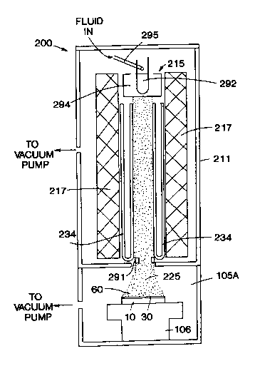
Referring to the drawing, there is shown a diagram of a
plasma jet deposition system 200 of a type which can be utilized
in practicing an embodiment of the invention. The system 200 is
contained within a housing 211 and includes an arc-forming
section 215 which comprises a cylindrical cathode holder 294, a
rod-like cathode 292, and an injector 295 mounted adjacent the
cathode so as to permit injected fluid to pass over the cathode
292. A cylindrical anode is represented at 291. In the
illustrated system the input fluid may be a mixture of hydrogen
and methane. The anode 291 and cathode 292 are energized by a
source of electric potential (not shown), for example a DC
potential. Cylindrical magnets, designated by reference numeral
217, are utilized to control the plasma generated at the arc
farming section. The magnets maintain the plasma within a narrow
column.until the hot gases reach the deposition region 60:
Optional cooling coils 234, in which a coolant can be circulated,
can be located within the magnets.
In operation, a mixture of hydrogen and methane is fed to
the injector 295, and a plasma is obtained in front of the arc
forming section and accelerated and focused toward the deposition
region. The temperature and pressure at the plasma formation
region are typically in the approximate ranges 1500-15,000
degrees C and 100-700 tort, respectively, and in the deposition
8
CA 02153184 2001-04-04
region are in the approximate ranges 800-1100 degrees C and
0.1-200 torr, respectively. As is known in the art, synthetic
polycrystalline diamond can be formed from the described plasma,
as the carbon in the methane is selectively deposited as diamond,
and the graphite which forms is dissipated by combination with
the hydrogen facilitating gas. For further description of plasma
jet deposition systems, reference can be made to U.S. Patent No.s
4,471,003, 4,487,162, and 5,204,144. It will be understood that
other suitable types of deposition equipment, including other
types of CVD plasma deposition equipment, can be used in
conjunction with the features of the invention.
The bottom portion 105A of the chamber has a base 106 on
which can be mounted a substrate 10 on which the synthetic
diamond is to be deposited. The base can include a temperature
controller. The substrate may be, for example, molybdenum,
tungsten, or graphite. Molybdenum, and its alloys such as TZM,
which contains relatively small percentages of titanium and
zirconium, is presently preferred. Reference can be made, for
example, to U.S. Patent No. 5,314,652, assigned to the same
assignee as the present Application, which describes
considerations of roughness of the substrate with regard to
appropriate holding and release of the diamond during and after
deposition, and also describes the advantageous use of an
interlayer (e.g.'illustrated at 30 in Figure 1), such as a
titanium nitride interlayer, for coating the substrate on which
9
_.
the synthetic diamond is to be deposited and ultimately released.
The substrate can be tilted and rotated during deposition as
described, for example, in U.S. Patent No. 5,204,144.
rvar,t7~7 L~C
In an example with a flat deposition surface, the target
substrate is a flat 4 inch diameter TZM disc which is tilted and
rotated during deposition. The deposition conditions, for
equipment of the general type shown in Figure 1, are as follows:
Plasma jet angle 15 degrees
Substrate rpm 2000
Offset (axis of jet from 3cm
center of substrate)
Temperature at substrate 900° C
Power 37kW
I5 Enthalpy 46 kJ/g H2
Pressure 13 torr
Methane concentration 0.1 percent
Hydrogen concentration balance
Deposition is continued until a synthetic diamond thickness of
about 380 um is obtained. The sample is cooled, released from
the substrate, and observed to have a convex bow, as viewed from
the deposition side. The sample is cut, with a laser, into 13 mm
squares and determined to have a radius of curvature of about 5.3
m.
In a further example, to reduce the bow, a concave substrate
is employed. In this case, the TZM substrate is provided with a
concave deposition surface. Machining and polishing is used to
obtain a substantially spherical contour having a radius of
IO
curvature of about 5.3 m. Deposition is implemented using the
same equipment and deposition conditions as in the prior example
to obtain a synthetic diamond sample having a thickness of about
380 ~cm. The sample is cut, with a laser, into 13 mm squares and
determined to have a radius of curvature of greater than 50 m;
i.e., much flatter than the sample made on a flat substrate.
11