Note: Descriptions are shown in the official language in which they were submitted.
2153273 GID-836
RING OSCILLATOR WITH FREOUENCY CONTROL LOOP
Field of the Invention
This invention relates to an oscillator system which
operates at a frequency which can be accurately set, and to a
method of operation thereof.
Background of the Invention
There are numerous electronic circuit applications where,
for proper operation, it is necessary to provide precise
timing or synchronization of one portion of a circuit with
another. Such timing is conveniently provided by a local
oscillator whose frequency is sufficiently accurate for the
requirements of the circuit being timed or ~ynchronized.
Depending on the degree of accuracy required, an oscillator
may be very simple and inexpensive where frequency range can
have wide latitude on the one hand, or relatively complex and
expensive where a high degree of accuracy (less than a few
percent error) in frequency is required. It is desirable to
have an oscillator which is both simple and inexpensive and
which operates at an accurate frequency.
Complementary metal oxide semiconductor (CMOS)
manufacturing technology is highly developed, and for many
applications, is the technology of choice in designing and
implementing large scale integrated circuits.
Various kinds of oscillators have been used for on-board
timing of other circuitry on a CMOS integrated circuit (IC).
One kind of oscillator which lends itself particularly well to
implementation by CMOS technology is a ring oscillator. In
2153~7~ GID-836
this kind of oscillator there are no inductor-capacitor tuned
circuits which in other oscillators are used to accurately set
the frequency of operation. Instead of tuned circuits, a ring
oscillator has an odd number of identical and very simple
inverting stages connected in series, with an output of each
stage coupled to an input of the next stage and with the
output of the last stage coupled to the input of the first
stage. In one embodiment each stage is an inverter having a
pair of serially connected complementary metal-oxide-
semiconductor (MOS) transistors whose output switches to ahigh level, a ~1", when a low level, a "O" is applied to the
input thereof, and ~witches to a n o n when a n 1 n is applied to
the input thereof. The frequency of operation of this type of
o~cillator i~ determ;neA by the speed of progression of a
switching event of ~1~ to ~0~, and ~0~ to ~1 n from one stage
to another around the ring, and by the number of stages.
A conventional ring oscillator implemented in CMOS
technology as part of an IC chip may have its own frequency of
operation within a very wide range of frequencies. Thus, by
way of example, in one ring oscillator currently being
manufactured as part of a CMOS IC chip, the difference in
frequency of the o~cillator of one chip from the frequency of
the oscillator of another supposedly identical chip can be as
great as 3 to 1. This wide range of frequency of operation is
caused by physical and ~;m~n~ional variations inherent in the
manufacturing process and by normal temperature and supply
voltage changes. Obviously, where precise timing of a circuit
2153273 GID-836
is required (e.g., frequency accuracy to within a few
percent), such a wide frequency range as this is unacceptable.
It i8 desirable to have a CMOS ring oscillator which is
relatively inexpensive and whose frequency can be set to a
desired level of accuracy. The present invention provides an
effective and inexpensive solution to this problem of accuracy
in frequency of operation of ring oscillators.
Summary of the Invention
In one illustrative embodiment of the invention there is
provided an oscillator system implemented entirely in CMOS
technology as part of an integrated circuit (IC) chip. The
oscillator system comprises a ring oscillator (ROSC), a logic
counter and comparator (LCC) unit, a bias unit, a multiplexer,
and a memory. The operating frequency of the ring oscillator
i8 very accurately controlled automatically by a ~ettable bias
current applied to it by the bias unit. The latter in turn is
controlled by the LCC unit which operates initially to compare
the frequency of the ROSC with that of an external reference
clock signal (REF CLOCK). If the frequency of the ROSC is
slower than that of the reference clock signal, the LCC
automatically controls the bias unit to increase, by a
selected number of small digital increments, the current
applied to the ROSC to thereby increase its frequency to match
that of the reference clock. Conversely, if the frequency of
the ROSC is higher than that of the reference clock, the bias
current is automatically decreased by a suitable number of
small step-like increments thereby decreasing the frequency of
21~3~73
GID-836
the oscillator (ROSC) until it matches that of the reference
clock. Thus by increasing or decreasing in small increments
the bias current applied to the ring oscillator, its frequency
can be precisely matched to that of the reference clock. Once
the bias current has been adjusted to that value which gives a
frequency of operation of the ring oscillator that accurately
matches the frequency of the reference clock signal, the
digital settings of the bias unit which control the bias
current are entered into the memory and the reference clock
gignal i8 disconnected. Thereafter, even though main power
for the IC chip and the oscillator system is disconnected, the
memory retains the appropriate d-igital settings for the bias
unit 80 that when power is restored, the necessary value of
bias current is once again applied to the ring oscillator 80
as to generate the needed frequency of oscillation. Thus, the
ring oscillator will operate thereafter, within very close
limits, at that frequency previously determ;ned by the
reference clock.
The ROSC is integral with the IC chip and therefore there
is added security against a non-authorized person from easily
determ;n;ng its exact frequency of operation. Knowledge of
the frequency might enable someone to gain unauthorized access
to restricted information such as a pay-per-view cable TV
channel.
The present oscillator system permits the automatic,
immediate and very accurate setting of the frequency of the
ring oscillator on each IC chip even though manufacturing
215~273
- GID-836
tolerances and component variations would otherwise cause
their respective uncorrected frequencies to differ
considerably (e.g., typically by more than 2 to 1).
Viewed from another aspect, the present invention is
directed to an oscillator system comprising an oscillator,
reference clock means, clock counter and control means, logic
means, and bias means. The oscillator has a plurality of n
essentially identical inverting stages each having an input
and an output with the output of each stage being coupled to
the input of the next stage and with the output of a last
stage being coupled to the input of a first stage, where n is
an odd integer greater than one. Each of the n stages
comprises capacitor means for selectively storing electrical
charge, an adjustable source of electrical charge coupled to
the capacitor means, and switch means, which is coupled to the
capacitance means, for selectively facilitating
charging/discharging of the capacitive means 80 as to control
frequency and corresponding time period of an output signal
generated by the oscillator at the oscillator output during
operation. The reference clock means receives a reference
clock signal having a preselected frequency and corresponding
time period. The counter and control means separately counts
over a same period of time a number of oscillator time periods
and a number of reference clock signal time periods and
generates a count difference between the respective counts of
the time periods. The logic means, which is responsive to the
count difference generated by the counter and control means,
215 327 3 GID-836
generates control signals corresponding to the count
difference. The bias means, which is responsive to the
control signals generated by the logic means and is coupled to
the sources of electric charge, controls the respective
sources of electric charge of the oscillator stages such that
the frequency of the oscillator is adjusted in accordance with
the count difference so as to ensure that the oscillator
frequency is in close agreement with the frequency of the
reference clock signal.
Viewed from still another aspect, the present invention
i8 directed to an oscillator system comprising a ring
oscillator (ROSC), bias means, and logic counter comparator
(LCC) means. The ring oscillator (ROSC) comprises an odd
plurality of n inverting stages, each stage having a constant
current source transistor with a control electrode and having
a switch transistor pair with a control electrode. An output
of the switch transistor pair is coupled in series with the
current source transistor. Each stage has an output coupled
to a control electrode of a switch transistor pair of the next
stage with the output of a last stage being coupled to the
electrode of the switch transistor of a first stage. The bias
means, which is coupled to the control electrodes of the
current source tran8i8tors of the n stages, determines the
current through each current source transistor. The logic
counter comparator (LCC) means, which is coupled by an output
thereof to an input of the bias means, compares the frequency
of the ROSC with that of a reference clock signal, determines
2 1 7 3 ~ 7 3 GID-836
a numerical difference between the two frequencies, and
generates at the output thereof signals representative of such
difference such that the bias means generates signals which
are coupled to the ROSC that ensure that the oscillator
frequency is in close agreement with the frequency of the
reference clock signal.
Viewed from still another aspect, the present invention
is directed to a method of operating an oscillator having an
odd plurality of n inverting stages, each stage having an
input, an output, a capacitor, an adjustable source of current
for charging the capacitor in the following stage, and a
switch for discharging the capacitor in the following stage,
the output of a first stage being coupled to an input of the
second stage and so on to the nth stage whose output is
coupled back to the input of a first stage. The method
comprising a first step of charging the load capacitor of a
first stage from the adjustable current source thereof. A
second step of discharging the load capacitor of a second
stage through the switch of that second stage in response to
the charging of the load capacitor of the first stage. A
third step of charging the load capacitor of a third stage
from the adjustable current source thereof in response to the
discharging of the load capacitor of the second stage, and 80
on from one successive stage to the next continually around in
a ring of the n stages. A fourth step of comparing a
frequency of the oscillator with a frequency of a reference
clock signal by simultaneously counting in separate counts a
21532~ 3 GID-836
number of time periods of oscillation of the oscillator and
the reference clock signal until a predetermined count is
reached in either count and then discontinuing counting. A
fifth step of determ;n;ng a count difference between the
counts. A sixth step of providing for incremental changes in
a number of steps in the currents provided by the adjustable
sources of current in the plurality of stages; and a seventh
step of making changes in the currents provided by the
adjustable sources of current in accordance with the
determ;ne~ count difference such that the frequency of
oscillation of the oscillator is adjusted to closely match the
frequency of the reference clock-signal.
Viewed from still another aspect, the present invention
iB directed to a method of controlling the frequency of
operation of an oscillator. The method comprises a first step
of arranging an odd plurality of n capacitors with charging
current sources and discharging switches in a ring
configuration to form an oscillator. A second step of using
charging currents to selectively charge a first capacitor of
the n capacitors to cause a discharging through a switch of a
second capacitor of the n capacitors, and the discharging of
the second capacitor to cause charging currents to charge a
third capacitor of the n capacitors, and 80 on in sequence to
an nth capacitor and then back to the first capacitor in a
continual sequence of capacitor charging and discharging
events which results in an output signal having a frequency
and corresponding time period. A third step of comparing the
2153273 GID-836
frequency of the oscillator with the frequency of a reference
clock signal to determine the difference therein; and a fourth
step of adjusting the values of charging currents into the
capacitors in accordance with the determined difference
between the frequency of the oscillator and the frequency of
the reference clock signal 80 as to cause the frequency of the
oscillator to be adjusted so as to be close to the frequency
of the reference clock signal.
A better underst~n~;ng of the invention together with a
fuller appreciation of it8 important advantage8 will best be
gained from a study of the following description given in
conjunction with the accompanying drawings and claim8.
Brief Description of the Drawings
FIG. 1 is a schematic representation in block diagram
form of an oscillator system in accordance with the present
invention;
FIG. 2 is a schematic representation of a ring oscillator
(ROSC) useful in the oscillator system of FIG. 1;
FIG. 3 is a schematic representation of a bias unit
useful in the oscillator system of FIG. 1;
FIG. 4 is a schematic representation, in block diagram
form, of a logic counter comparator (~CC) unit useful in the
oscillator system of FIG. 1;
FIG. 5 shows how FIGS. SA and 5B are coupled together;
FIGS. 5A and 5B show a detailed circuit diagram of a ring
oscillator (ROSC) useful in the oscillator system of FIG. 1;
- 21S3273 GID-836
FIG. 6 shows how FIGS. 6A and 6B are coupled together;
FIGS. 6A and 6B show a detailed circuit diagram of a bias unit
uReful in the oscillator system of FIG. 1.
FIG. 7 shows a detailed diagram of a logic circuit useful
for performing the functions of a control logic unit and a
m; n; ml~m count detector of FIG. 4; and
FIG. 8 shows how FIGS. 8A and 8B are coupled together;
FIGS. 8A and 8B show a detailed diagram of a logic and
switching circuit forming another portion of the logic counter
cn~r~rator (LCC).
Detailed Description
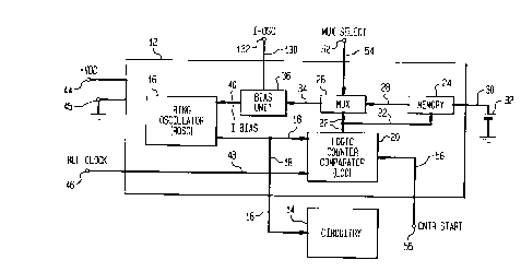
Referring now to FIG. 1, there is shown, in block diagram
form, an oscillator system 12 (shown within a solid line
rectangle) in accordance with the present invention which has
an output which is coupled via a lead 18 to circuitry 14.
Oscillator system 12 generates on lead 18 a signal having a
frequency which is needed by circuitry 14. A battery 32 is
shown coupled by a positive term; n~l thereof to a memory 24 of
oscillator 12.
The oscillator system 12 comprises a ring oscillator
(ROSC) 16, a bias unit 36, a multiplexer (MUX) 26, the memory
24, and a logic counter comparator (LCC) 20. The lead 18 also
couples an output of the ring oscillator 16 to an input of the
LCC 20. An output of LCC 20 is coupled via a common lead 22
to an input of memory 24 and to an input of multiplexer (MUX)
26. The memory 24 is connected via a lead 28 to another input
of the MUX 26. Battery 32 insures retention of data in the
21~273
GID-836
memory 24 when external power to the oscillator system 12 is
disconnected. Memory 24 could be a nonvolatile type of memory
and would not require a battery 32 to retain stored memory for
a useful period of time. An output of the MUX 26 is connected
via a multi-conductor lead 34 to the bias unit 36 which in
turn is connected via a lead 40 to the ROSC 16. During
operation of oscillator system 12 a current I-bias flows from
an output of bias unit 36 via a lead 40 to an input of ROSC
16. The current I-bias controls the frequency of operation of
ROSC 16. The oscillator system 12 has a pair of power supply
term; n~ 1 8 44 and 45 to which external voltages, such as +VDD
and ground, respectively, are selectively connected.
Similarly, oscillator system 12 has a term; n~l 46 (REF CLOCK)
to which an external reference clock signal (not shown) having
a preselected frequency can be selectively connected. The
term; n~l 46 is connected via a lead 48, to an input of the LCC
20. The oscillator system 12 also has a term; n~l 52 to which
an external ~MUX SELECT" signal can be selectively applied to
control via a lead 54 the setting of the MUX 26. When
temporarily set in one position, the MUX 26 applies digital
control data from the LCC 20 directly to the bias unit 36.
When set in another (long term) position, the MUX 26 applies
the contents of the memory 24 to the bias unit 36. The
contents of memory 24 are the same as the digital control data
from the LCC 20 right after a calibration process (described
hereinafter). The calibration process is initiated by a start
signal (from a source not shown) applied to a terminal (CNTR
21S32~ 3 GID-836
START) 55 and via a lead 56 to the LCC 20. A terminal 132 is
coupled via a lead 130 to bias unit 36. During operation of
oscillator system 12 a current I-OSC is established in bias
unit 36 which flows via lead 130 into term;n~l 132. A
constant current source (not shown) is coupled to terminal 132
and is typically a band gap current generator which generates
a constant current level substantially independent of power
supply and temperature variations over useful ranges.
Oscillator system 12 is typically formed in an integrated
circuit chip. Circuitry 14 can optionally be formed on the
same integrated circuit chip as oscillator system 12 and may
comprise the largest portion of the chip. In a preferred
embodiment oscillator system 12 is formed in an integrated
circuit chip using CMOS components and circuitry 14, which
would also use CMOS components, is also formed in the same
integrated circuit chip. The operation of the circuitry 14 is
determ;ne~ by whatever application it is designed for. The
oscillator system 12 provides timing or synchronization via
the lead 18 to the circuitry 14.
An overall view of the operation of oscillator system 12
is as follows. When external power (+VDD and ground) is
applied to term;n~ls 44 and 45, respectively, of the
oscillator system 12, the ROSC 16 oscillates at a frequency
determ;ne~ by its basic design. This frequency is controlled
by variables such as voltage and temperature, by physical and
~;men~ional differences due to manufacturing tolerances, and
by a control current applied to it via the lead 40 from the
2 1 ~ 3 2 7 3 GID-836
bias unit 36. Because of these factors and without any
control of the current from the bias unit 36, the ROSC 16 may
operate at a frequency greatly different from the frequency
desired for operation of circuitry 14.
The design of the ROSC 16 is such that by incrementing
control current on the lead 40 above or below a median or
nomi n~l value, the frequency of the ROSC 16 can be adjusted to
a desired value (within a few percent). To make this
adjustment, a reference clock (not shown), operating precisely
at the desired frequency, is coupled to the "REF CLOCK"
term;n~l 46. When a start signal is applied to the t~rm;n~l
55, the calibration process begins and the LCC unit 20
automatically compares the frequency of the reference clock
with that of the ROSC 16. If the frequency of the ROSC 16 is
higher than that of the reference clock, the count of time
periods (cycles) of oscillation of the ROSC 16 starting at a
given time reaches a predetermined number (e.g., ~ln) somewhat
sooner than the count of time periods of the reference clock.
On the other hand, if the frequency of the ROSC 16 is lower
than that of the reference clock, the count of time periods of
the reference clock reaches a predetermined number (e.g., "ln)
somewhat sooner than the count of time periods of the ROSC 16.
In either event, the difference in the numbers of cycles
counted between the two frequencies is then detected and
decoded within the LCC 20. The LCC 20 then applies, according
to a preselected algorithm, a number of separate digital "on"
or ~off~ ~ignals via the common multi-conductor lead 22
2153~73 GID-836
through the MUX 26 to the bias unit 36. At the same time
these digital signals are also provided to and stored in the
memory 24.
The digital signals from the LCC 20 control the settings
of respective switches (not shown here but shown in FIG. 3 and
described in detail hereinafter) within the bias unit 36. In
this way the control current applied via the lead 40 from the
bias unit 36 to the ROSC 16 is set to a value which causes the
frequency of operation of the ROSC 16 to match (within a few
percent) the frequency of the reference clock. These same
digital signals from the LCC 20 are stored in the memory unit
24 80 that, even though main power to the oscillator system 12
is disconnected and the reference clock removed, when power iB
restored, these digital signals are automatically re-applied
from memory unit 24 through the MUX 26 to the bias unit 36 and
the proper value of control current is again applied to the
lead 40. The ROSC 16 thus operates at the desired frequency
(i.e., that of the reference clock even though it is no longer
present).
Oqcillator system 12 is fully automatic-and very
accurate. The operation of comparing frequencies within the
LCC 20 and of setting the control current on the lead 40 to
the ROSC 16 takes only a small fraction of a second. This is
called the calibration process. Once the frequency of the
ROSC 16 has been set, it remains set at the frequency of the
reference clock until, if desired, it is reset by repeating
the above-described process of compari~on with a reference
2153273 GID-836
clock (calibration process) by applying a new CNTR START
signal to the term; n~l 55 and the reference clock frequency to
the termi n~l 46.
Referring now to FIG. 2, there is shown, in basic
schematic form one illustrative embodiment of the ROSC 16 of
FIG. 1. Additional details will be given hereinafter. AS
shown here, the ROSC 16 has "n" essentially identical
switching stages 60 (only stage 1, stage 2, and stage "n"
being shown). Respective elements of each stage 60 are given
the same reference numbers. The input control current from
the bias unit 36 applied to the ROSC 16 via the lead 40 is
here identified as "I-biasn. Each switching stage 60
comprises a constant current generator 62, the current from
which i8 controlled by "I-bias n, The current from the
15 generator 62 flows in the direction of an arrow 65. The
current generator 62 is connected in series with a switch 66
having an upper term; n~l 67 connected to the current generator
62 and having a lower terminal 68 connected to ground. A
capacitor 70, belonging to the following (next) stage and
connected in parallel with the switch 66, has an upper
electrode 72 connected to the term; n~l 67 and has a lower
electrode 74 connected to the terminal 68 (ground). The
capacitor 70 has in parallel with it an impedance 78, which
represents the impedance of a transistor (not shown here)
which at times is "on" and at other times "off n, An output of
each of the ~n" stages is coupled to an input of the next
stage via a conductor 86 with the output of the "nth" stage
2 1 5 3 2 7 3 GID-836
coupled to the input of the first (1) stage. These and other
elements of the ROSC 16 will be described in detail
hereinafter.
The switch 66 of Stage 1 of the switching stages 60 is
shown, by way of example, in the "open" position indicated
here by the position of a solid line 82. As will be explained
hereinafter these switches 66 are in reality transistors (not
shown here). It will be noted, in the example given here,
that the switch 66 of Stage 2 i8 in the "closed" position
(indicated by the position of the solid line 82) and 80 on, to
Stage ~n" where the position of the switch 66 is closed
(indicated by the position of the line 82). There are always
an ~odd~ number "n" of the stages 60 (seé FIG. 2).
In a preferred embodiment, the capacitor 70 of each stage
60 represents the interelectrode parasitic capacitances of
transistors (not shown here) associated with that stage. The
capacitor 70, while typically very small (e.g., femtofarads),
nonetheless affects the switching time of each stage 60 in
going from ~off~ (digital ~On) to "on" (digital "ln) and vice
versa (discharging time is as important as charging time).
Thus, when the switch 66 of Stage 1 is initially switched from
closed to open, the charge and voltage on the capacitor 70 of
Stage 2 are substantially zero (digital n o n ) . AS charging
current begins to flow from the current generator 62 of Stage
1 in the direction of the arrow 65 around the now-open switch
66, the charge and voltage across the capacitor 70 of Stage 2
~~ 21~3273 GID-836
builds up to a full value (digital n 1~ ) which remains so long
as the switch 66 of Stage 1 rPmA; n~ open.
After a short time, the charge on the capacitor 70 of
Stage 2 reaches a level which causes the respective switch 66
of Stage 2 to switch from an open to a closed position. When
the switch 66 of the Stage 2 is closed, the capacitor 70 of
Stage n is discharged through the respective switch 66 of
Stage 2 and a digital n o n is thereupon stored on this
respective capacitor 70 of Stage n. When the voltage on the
capacitor 70 of the Stage n has dropped to a low enough level
(near zero), the respective switch 66 of the Stage n (here,
Stage "n" i8 after Stage 2, Stage 3 not being shown) is
actuated from a closed to an open position, and the respective
capacitor 70 of that odd numbered stage 60 is charged to a
digital n 1 n . This sequential actuation of the respective
switches 66 and the charging and discharging of the respective
capacitors 70 of the stages 60 progresses during a cumulative
time through the series of stages 60 from the first to the
last (Stage "1~ to Stage nnn).
Stage ~n" is connected via a lead 90 to an input of a
buffer-amplifier 92 whose output is coupled to a lead 18 (see
FIG. 1) where the clock output signal (CLKO) of the ROSC 16 is
produced. A switching signal from Stage "n" is applied via
the respective conductor 86 to the switch 66 of Stage 1. When
the switch 66 of Stage "n" switches "open" to store a digital
~1~, the switch 66 of Stage 1, after a short delay, switches
to a ~closed" position which effectively stores a digital ~0
21S32~ GID-836
in Stage 1. When the switch 66 of Stage "n" switches closed,
which stores a ~o n in Stage "n", the switch 66 of Stage 1
switches to an "open" position and 80 on in sequence
continuously around the ring of stages 60.
It will be appreciated by those skilled in the art that
the time required for the respective capacitor 70 of a
switching stage 60 to charge to a digital n 1 n or to discharge
to a digital "0" through the controlled switch 66 is a
function among other things of the amplitude of the charging
current applied to it by the respective current generator 62
of that stage. This current from the generator 62 is
controlled by the I-bias current. An important feature of the
invention is that the operating frequency of the ROSC 16
(output signal CLKO) is accurately adjusted by controlling the
amplitude of the I-bias current. This will be explained in
greater detail hereinafter. Thus the frequency of the output
signal CLKO of the ROSC 16 is electronically controlled
automatically to match (within a few percent) the frequency of
a reference clock in spite of circuit component variations and
of normal operating changes in supply voltage and temperature.
Referring now to FIG. 3, there is shown an illustrative,
abbreviated schematic form of the bias unit 36 of FIG. 1.
Output control current I-bias from the bias unit 36 is applied
via the lead 40 to the ROSC 16 (see also FIGS. 1 and 2). The
bias unit 36 comprises a number of current stages "I-l"
through "I-N", each current stage being generally indicated at
100, and a current mirror (CM) unit 102 which serves also as a
21~32~ ~ GID-836
current divider. These "N" current stages 100 (only three, I-
1, I-2, and I-N, of which are shown) are typically identical
to each other and corresponding elements of each of the stages
100 have the same respective reference numbers.
Each current stage 100 comprises a series connection of a
first current generator 104, a first (upper) switch 106 (shown
open), a second (lower) switch 108 (shown open) and a second
current generator 110. The switch 106 has an upper term;n~l
112 connected to the generator 104, and a lower term; n~l 114
connected to the lead 40 and to a term;nal 134. Current flows
from the first generator 104 (when the switch 106 is closed)
in the direction of an arrow 116. The lower switch 108 has an
upper t~rm;n~l 120 connected to the lead 40 and to the
term;n~l 134 and a lower term;n~l 122 connected to the second
generator 110. Current flows from the generator 110 (when the
switch 108 is closed) downward to ground in the direction of
an arrow 124. All of the upper switches 106 and the lower
switches 108 of the Stages I-l through I-N may be open at the
same time (as shown here), but whenever any upper switch 106
is closed, all of the lower switches 108 are open, and vice
versa. Thus when an upper switch 106 of any current stage 100
is closed, the current from the respective current generator
104 flows in the direction of the arrow 116 into the lead 40,
and all of the lower switches 108 are open. When a lower
switch 108 of any current stage 100 is closed, current from
the respective lower current generator 110 flows in the
21~327 3 GID-836
direction of the arrow 124 out of the lead 40 to ground. At
this time all of the upper switches 106 are open.
The CM unit 102 is connected via a lead 130 to an input
terminal 132. A reverse current "I-OSC", which rPm~;ns highly
constant even when there are normal voltage supply variation
and temperature variations, is applied to the input terminal
132 from a current source (not shown). The current ~I-OSC"
flows in the direction of an arrow 133. The CM unit 102
-applies to the term;n~l 134, a constant current "I-0" which
flows in the direction of an arrow 136 into the lead 40. The
current n I- O n may, for example, have an amplitude equal to
that of "I-OSC", and is highly stable. The CM unit 102
controls the amplitude of the respective currents (as will be
explained in detail hereinafter) from each of the upper
current generators 104 and from each of the lower current
generators 110, as indicated here by the upper dashed line
arrows 140 respective to the upper generators 104, and the
lower dashed line arrows 142 respective to the lower
generators 110. There may be, for example, eight current
stages 100, and each current generator 104 or 110 may produce
a small, exactly determined fraction of the current "I-0"
applied to the lead 40 by the CM 102.
Depending on the controlled closings of one or more of
the upper switches 106, or alternatively the closings of one
or more of the lower æwitches 108 of the current stages 100,
current is either incrementally added to the lead 40 in
addition to the current ~I-O" from the CM unit 102, or current
21532~ 3 GID-836
is incrementally subtracted from the current on the lead 40.
The output current n I-bias n on the lead 40 is thus the current
n I O n with small, precisely determined incremental additions
(or subtractions) of current provided by the current stages
100. The settings of the upper switches 106 and the lower
switches 108 are controlled, as will be explained in detail
hereinafter, by separate "on" or "off n digital signals applied
respectively to the switches via the multi-conductor lead 34
(see FIG. 1). Here (FIG. 3)~ the lead 34 is illustrated as
having a multiple conductor upper portion 146 and a multiple
conductor lower portion 148.
Referring now to FIG. 4, there is shown an illustrative
embo~;ment of functional portions in block form of the LCC
unit 20 of FIG. 1. me LCC 20 comprises a control logic (CL)
portion 200, an oscillator counter (OC) 202, a reference clock
counter (RCC) 204~ a m;n;mllm count detector (MCD) 206~ and a
switch logic and output latches (SLOL) portion 208. Separate
digital ~on" or ~off n output signals from the SLOL 208 are
applied to the lead 22 (see also FIG. 1) which is shown here
as having an upper, multiple conductor portion 210, and a
lower multiple conductor portion 212. These digital signals
are applied via their respective conductors in the lead 22 to
the memory unit 24 and the MUX 26 (see FIG. 1) and thence via
separate conductors in the lead 34 at the output of the MUX 26
to the bias unit 36. These digital signals from the SLOL 208
control the respective settings of the switches 106 and 108 of
21S327~ GID-836
the current Stages I-1 through I-N of the bias unit 36, as was
previously explained (see FIG. 3).
The CL portion 200 of the LCC 20 receives via the lead 18
signals from the ROSC 16, and receives via the lead 48 signals
from a reference clock (not shown) applied to the terminal 46.
With a "start" c~mmAn~ (CNTR START applied to the terminal
55), the CL portion 200 applies via a lead 216 signals from
the ROSC to the OC 202, and applies via a lead 218 signals
from the reference clock to the RCC 204. Counters OC 202 and
RCC 204 are identical and each provides a cumulative count of
the number of cycles counted from the instant of starting of
the respective ROSC and reference clock signals applied to the
counters. By way of example, the counters 202 and 204 are 8-
bit binary counters (well known in the art) able to count up
to 256 time periods (cycles) of the oscillating signals
applied to them. The output count of the OC 202 is applied
via a multi-conductor common lead 220 to the MCD 206 and to
the SLOL 208. The output count of the RCC 204 is applied via
a multi-conductor common lead 222 to the MCD 206 and the SLOL
208. At ~start" (when CNTR START is applied to terminal 55),
each counter is initially set at the binary equivalent of
decimal 255 and thereafter counts down to zero (m;n;mllm
count). When either counter OC 202 or RCC 204 reaches or
almost reaches "zero" count (the other counter will still have
a non-zero count), this zero is detected by the MCD 206 which
then via a lead 224 signals the CL 200 to "stop" input signals
on the leads 216 and 218 to the respective counters OC 202 and
215327 ~ GID-836
RCC 204. The respective output counts of the OC 202 and the
RCC 204 are thus "frozen" when the CL 200 receives a "stop" on
zero count signal from the MCD 206. While the counters OC 202
and RCC 204 are counting, their respective binary output
counts are being applied on-the-fly to the SLOL 208. The SLOL
208 continuously decodes the binary counts and applies on
subsequent c~mmAn~ from the CL 200 via the lead 230, when the
counts are "frozen", a selected sequence of digital "on" or
~Off n output signals to respective conductors of the output
lead 22.
On receipt of a "stop" signal to the CL 200 from the MCD
206 at n zero n count from one or the other counter OC 202 or
RCC 204, both the zero and the non-zero count in the counters
are "frozen" and decoded. Simultaneously, the CL 200 via a
lead 230 signals the SLOL 208 to "latch" separate steady-state
digital "on" or "off n signals onto the multi-conductor output
lead 22. The sequence of these digital signals "on~ and "off~
corresponds to the decoded non-zero count in accordance with a
predetermined algorithm, as will be explained hereinafter. If
the residual non-zero count rPmA;n~ in the OC 202, the ROSC 16
has a frequency slower than that of the reference clock. If
the non-zero count rPmA;n~ in the RCC 204, the ROSC 16 has a
frequency faster than that of the reference clock. The SLOL
208 is thus able to tell from the "frozen" non-zero binary
count on either the lead 220 or the lead 222 (the count on the
other lead is zero) whether to apply a digital "on" signal or
signals to a respective conductor or conductors in the upper
215327 3 GID-836
portion 210 of the output lead 22, or to a respective
conductor or conductors in the lower portion 212 of the lead
22. The above description of the LCC 20 gives an overview of
its organization and mode of operation. A further explanation
of the operation of the LCC 20 and specific details of its
structure and organization will be given hereinafter.
Referring now to FIGS. 5A and 5B, there i9 shown a
specific circuit diagram of a preferred embodiment of the ROSC
16 of FIGS. 1 and 2. The ROSC 16 here comprises five
substantially identical switching Stages "1" through "5" (an
odd number of stages) shown within ~Ashe~ line boxes 300.
Bach stage 300 here is equivalent to a switching stage 60
shown schematically in FIG. 2. Each stage 300, for example
Stage 1, comprises a p-~h~nnel field effect transistor 302
connected in current series with an N-ch~nn~l field effect
transistor 304. An N-~h~nnel field effect transistor 306,
with its drain and gate connected together so as to function
as a diode, is coupled to the transistor 304 and is located
within the same stage. The transistors 304 and 306 are
connected in an N-channel current mirror arrangement, the
operation of which is described hereinafter. Each of
transistors 302, 304 and 306 has a drain, a source, and a
gate. The drain and source may be denoted as first and second
or second and first outputs of the transistor. Corresponding
elements in each of the stages 300 have been given the same
respective reference numbers.
21~ 3 27 3 GID-836
The transistor 302 has a source electrode 310 connected
to a common voltage bus 312 to which a supply voltage +VDD is
applied. The transistor 302 has a gate electrode 314
connected to a control voltage bus 316, and has a drain
electrode 318 connected to a term;n~l (node) 320. The
transistor 304 has a drain electrode 322 connected to the
term;n~l 320, has a gate electrode 324 connected to the
term;n~l 320 of the immediately preceding (driving) stage, and
has a source electrode 326 connected to a ground bus 328. The
transistor 306 has a drain electrode 330 and a gate electrode
332 both connected to the term;n~l 320 of the driving
(immediately preceding) stage and has a source electrode 334
connected to the ground bus 328. Transistor 306 is configured
as a diode and as such serves to act as a voltage clamp which
limits the voltage swing of t~rm;n~l 320 of the preceding
driving stage. This serves to reduce undesirable switching
noise in oscillator system 12. Parasitic capacitance
associated with transi~tors 302 and 304 of the driving stage,
and transistors 306 and 304 of the following stage, is shown
a~ a dashed line capacitor 329 which has a firYt plate coupled
to term;nAl 320 of the driving stage and has a second plate
coupled to ground bus 328. It is to be noted that the gate
electrode 324 of the transistor 304 in Stage 2 is connected
back to the term;n~l 320 of Stage 1, the gate electrode 324 of
the transistor 304 in Stage 3 connected back to the ter~;
(node) 320 of Stage 2, and 80 on, to Stage 5. The term;n~l
(node) 320 of Stage 5 is connected via a lead 336 to the gate
2153273 GID-836
324 of the transistor 304 of Stage 1. Thus the five stages
300 of the ROSC 16 are connected in a "ring".
Shown at the right in FIG. 5B is a P-channel field effect
transistor 346, having a drain electrode 348 connected to the
voltage supply bus 312, having a gate electrode 350 connected
to the voltage bus 316, and having a drain electrode 352. An
N-ch~nnel field effect transistor 354 has a drain electrode
356 connected in common to the drain electrode 352 of the
transistor 346 and to a lead 358, has a gate electrode 360
connected to the gate electrode 324 of the transistor 304 of
Stage 5, and has a source electrode 362 connected to the
ground bus 328. The lead 358 is-connected to an input of a
first amplifier-inverter 364 and coupled to an input of a
second amplifier-inverter 366 whose output i8 coupled to the
output lead 18 where the output signal CLKO of the ROSC 16 is
obt~;n~.
Shown at the left of FIG. 5A is a P-channel field effect
transistor 370 which has a source electrode 372 connected to
the voltage bus 312, and has a gate electrode 374 and a drain
electrode 376 both connected to the voltage bus 316. An N-
channel field effect transistor 380 has a drain electrode 382
connected in common to the drain electrode 376 of the
transistor 370 and the voltage bus 316, has a gate electrode
384 connected to the I-bias current lead 40 (see FIG. 2) and
has a source electrode 386 connected to the ground bus 328.
An N-channel field effect transistor 390 has a drain electrode
392 and a gate electrode 394 both connected in common to the
26
2153~3 GID-836
lead 40, and has a source electrode 396 connected to the
ground bus 328.
The control current I-bias flows from the lead 40 in the
direction of an arrow 398 through the transistor 390, which i8
diode-connected, and produces a control voltage on the gate
384 of the transistor 380 which in turn generates a current
proportional to the control current I-bias flowing through the
transistor 380 to ground. The current flowing through the
transistor 380 from the transistor 370, which is diode-
connected, produces in turn a voltage on the control voltagebu~ 316 which can be used to generate a current proportional
to the I-bias current. This voltage is preci~ely controlled
by the I-bias current. In effect, this arrangement transforms
the I-bias control current into a corresponding control
voltage on the voltage bus 316. The transistor 370 is
connected with the transistors 302 of the stages 300 in a
current mirror arrangement (well known in the art) to produce
respective currents in the transistors 302 of the stages 300
proportional to the current through the transistor 370. The
control voltage on the voltage bus 316 is determined by the
current through the transistor 370 which is proportional to
the I-bias current and in turn controls the respective
currents through the transistors 302. By way of example, the
current through the transistor 370 may be set to equal the I-
bias current by the current mirror comprised of the N-channel
transistors 390 and 380, and the respective currents through
- 215327~ GID-836
the transistors 302 of the stages 300 may each be made equal
to the current through the transistor 370.
As was explained in connection with FIG. 2, the current
available from the generator 62 to charge the load capacitor
70 of a stage 60 when its respective switch 66 is opened
determines the time required to charge the capacitor 70 to
full value. The discharging current when the switch 66 is
closed is also proportional to the current available from the
generator 62 (through the action of the N-ch~nnel current
mirror transistors 306 and 304), and determines the
discharging time. In FIGS. 5A and 5B no capacitor per se is
~hown and it is to be understood that the equivalent of the
capacitor 70 (FIG. 2) is the interelectrode capacity from the
term; n~l (node) 320 to ground for each stage 300. The
transistors 304 of the stages 300 of FIGS. 5A and SB
correspond to the switches 66 (FIG. 2) and the transistors 306
of FIGS. 5A and 5B correspond to the impedances 78 (FIG. 2).
The transistor 302 of each stage 300 of FIGS. 5A and 5B
corresponds to the current generator 62 (FIG. 2). The
respective current available from the transistor 302 of each
stage 300 is controlled by the I-bias current through the
voltage on the control voltage bus 316.
In a preferred embodiment, the size of the transistor 306
is made half that of the transistor 304 so that the transistor
304, when on, will want to conduct a current equal to twice
that of transistor 306. The current through the transistor
306 is equal to the current in transistor 302 of the preceding
2153273 GID-836
stage. Thus when the transistor 304 switches on, it will take
all of the current from the transistor 302 and more, which
helps to quickly pull the potential on the node 320 down
nearly to zero (ground potential). This discharge~ capacitor
329 and results in a digital n O 1l being stored in that
particular ~tage 300. When the transistor 304 switches off,
controlled current from the transistor 302 will in a short
time charge the load capacitances (capacitor 329) of this
stage 300 to a potential representing a digital "ln. This
potential is clamped to a relatively low value (typically only
slightly larger than the threshold voltage of an N-ch~nnel
device) by the diode-connected transistor 306. The charging
and discharging times of the interelectrode capacitances
(i.e., capacitor 329) are functions of the amplitude of the
current supplied by the transistor 302, as was explained
previously.
It will be seen from the circuit of the ROSC 16 shown in
FIGS. 5A and 5B that when the transistor 304 of Stage 1 of the
stages 300 switches ~on", the respective voltage of voltage
node 320 is pulled down to near ground potential (digital "on)
in a controlled time. This in turn pulls the gates 324 and
332 of the transistors 304 and 306 of the next stage 300,
Stage 2, to near ground potential and causes the transistor
304 of Stage 2 to turn "offn. When this occurs, the ter~;n~l
320 (and its interelectrode capacitances) of Stage 2 are then
(in a controlled time) charged to a high level (a digital
by the transistor 302 of Stage 2. The stages 300 may be
29
215327 3 GID-836
termed current steering inverters. The ROSC 16 and its
associated bias unit 36 operate in accordance with current-
steering logic. The switching from "1" to "0", and "0" to "1"
in turn from one stage 300 to the next stage 300 of the ROSC
16 is continuous, though each stage 300 is bi-stable. The
time required for a switching event to progress from one stage
to the next (which is controllable) and the number of stages
(which is predetermined) determine the frequency of operation
of the ROSC 16. The function of P-channel transistor 346 and
N-ch~nnel transistor 354 is to transfonm the current-steering
logic digital levels into regular CMOS logic digital levels.
mis is achieved by suitably setting the sizes of these
transistors with respect to each other.
Referring now to FIGS. 6A and 6B, there is shown a
preferred embo~;m~nt of the bias unit 36 of FIG. 3. The bias
unit 36 of FIGS. 6A and 6B comprises eight current-supply
stage n I -1 n through n I-8 n, each stage being shown within a
dashed line box generally indicated at 400. The stages 400
are substantially identical with each other, and corresponding
elements within each stage have been given respective
reference numbers. Each stage 400, Stage I-l for example, has
a P-channel field effect transistor 402, a first N-channel
field effect switch transistor 404, a second N-channel field
effect switch transistor 406 and an N-channel field effect
transistor 408. The transistor 402 has a source electrode 410
connected to a common supply voltage (+VDD) bus 411, has a
gate electrode 412 connected to a common control voltage bus
215327 3 GID-836
414, and has a drain electrode 416. The transistor 404 has a
drain electrode 418 connected to the drain electrode 416 of
the transistor 402, has a gate electrode 420 connected to an
input control term;nAl np lll, and has a source electrode 422
connected to a common output current bus 424. The transistor
406 has a drain electrode 426 connected to the output current
bus 424, has a gate electrode 428 connected to an input
control term;n~l ~M-l", and has a source electrode 430
connected to a drain electrode 432 of the transistor 408. The
transistor 408 has a gate electrode 434 connected to a common
control voltage bus 436, and has a source electrode 438
connected to a common ground bus-440. It is noted that the
input term;n~ls ~P-l" and ~M-l" are respective only to Stage
I-1; term;n~ls "P-2" and ~M-2~ apply to Stage I-2, and so on,
to term;n~ls ~P-8" and ~M-8" for Stage I-8. Steady state
digital "on" or "off n control voltage signals are applied to
respective ones of the terminals P-1 through P-8 and M-1
through M-8, as will be explained hereinafter, to set the
level of the current I-bias.
To the left in FIG. 6A are a P-channel field effect
transistor 442, a P-channel field effect transistor 444, a P-
ch~nnel field effect transistor 446 and an N-channel field
effect transistor 448. The transistor 442 has a source
electrode 450 connected to the supply voltage bus 411, and has
a gate electrode 452 and a drain electrode 454 connected to
the common lead 130 (also see FIGS. 1 and 3) which has a
term;n~l 132 connected thereto. During operation of
2153273 GID-836
oscillator system 12 a current I-OSC is established in bias
unit 36 of FIGS 6A and 6B which flows via lead 130 into
term;n~l 132. A constant current source (not shown) is
coupled to terminal 132 and is typically a band gap current
generator which generates a constant current level
substantially independent of power supply and temperature
variations over useful ranges. The transistor 444 has a
source electrode 458 connected to a supply voltage (+VDD)
term;nAl 460, has a gate electrode 462 connected to the common
lead 130, and has a drain electrode 464 connected to the
output current bus 424. During operation of bias unit 36 of
FIGS 6A and 6B a current I-O flows through lead 570 and forms
part of I-bias shown flowing in lead 40. The transistor 446
has a source electrode 466 connected to a voltage supply
(+VDD) term;n~l 468, has a gate electrode 470 connected to the
common lead 130, and has a drain electrode 472 connected to a
drain electrode 474 of the transistor 448. The transistor 448
has a gate electrode 476 connected to its drain electrode 474,
and has a source electrode 478 connected to a ground term;n~l
479. This same voltage +VDD can be connected to the bus 411
and the terminals 460 and 468.
To the right of the transistor 442, which is diode-
connected, is a current-divider current-mirror arrangement,
generally indicated within a dashed line box 480. This
arrangement 480 comprises four transistors: a P-channel field
effect transistors 482, an N-ch~nnel field effect transistor
484, a P-channel field effect transistor 486, and an N-channel
215327 ~ GID-836
field effect transistor 488. To the right of the N-channel
transistor 448 is a similar (but not identical) current-
divider current-mirror arrangement shown within a dashed line
box 490. The arrangement 490 comprises four transistors: P-
channel field effect transistors 492 and 496, and N-channel
field effect transistors 494 and 498.
The transistor 482 of the arrangement 480 has a source
electrode 502 connected to the supply voltage bus 411, has a
gate electrode 504 connected to a lead 130, and has a drain
electrode 506 connected to a drain electrode 508 of the
transistor 484. The transistor 484 has a gate electrode 510
connected to the drain electrode 508, and has a source
electrode 512 connected to a ground bus 514. The transistor
486 has a source electrode 516 connected to the supply voltage
bus 411, and has a gate electrode 518 and a drain electrode
520 both connected to the voltage bus 414. The transistor 488
has a drain electrode 522 connected in common to the drain
electrode 520 of the transistor 486 and to the voltage bus
414, has a gate electrode 521 connected in common to the gate
510 and the drain 508 of the transistor 484, and has a source
electrode 526 connected to the ground bus 514.
The transistor 492 of the arrangement 490 has a source
electrode 530 connected to a supply voltage (+VDD) bus 532,
and has a gate electrode 534 and a drain electrode 536 both
connected in common with a drain electrode 538 of the
transistor 494. The transistor 494 has a gate electrode 540
connected in common with both the drain electrode 474 and the
2153273 GID-836
gate electrode 476 of the transistor 448, and has a source
electrode 542 connected to a ground bus 544. The transistor
496 has a source electrode 546 connected to the voltage supply
bus 532, has a gate electrode 548 connected in common with
both the gate electrode 534 and the drain electrode 536 of the
transistor 492, and has a drain electrode 550 connected in
common with a drain electrode 552 of the transistor 498 and
the voltage bus 436. The transistor 498 has a gate electrode
554 connected to the drain electrode 552, and has a source
electrode 556 connected to the ground bus 544.
The output current bus 424 of the bias unit 36 is
connected at the left to a term~n~l 560 to which the lead 40
(I-bias) is connected. Current flows to the term;n~l 560 in
the direction indicated by an arrow 562. The common lead 130
is connected to the termin~l 132 to which the current ~I-OSC~
is applied. Current flows to the term;n~l 132 in the
direction of an arrow 566.
As mentioned previously, the current "I-OSC" is stable
with respect to supply voltage and temperature variations.
The flow of this current "I-OSC" through the transistor 442
establishes on the common lead 130 a stable voltage which can
be used to generate a current proportional to the current n I-
OSCn. The common lead 130 is connected to the gate 504 of the
transistor 482 which forms part of the current-divider
current-mirror arrangement 480. The voltage on the lead 130
generates a current proportional to the current I-OSC which
flows in series through the transistor 482 and the transistor
34
~ 327 ~ GID-836
484 which is diode-connected and serves as a current source.
The current through the transistor 488 is controlled by its
gate electrode 521 which i8 connected in common with the
drains 506 and 508 of the transistors 482 and 484,
respectively, and is proportional to the current I-OSC. The
transistor 488 is connected in series with the transistor 486
which is diode-connected as a current source. The transistor
486 is connected via the voltage bus 414 in a current-mirror
arrangement with the respective transistors 402 of the Stages
I-1 through I-8. The sizes of the transistors 482, 484, 486
and 488 of the arrangement 480 and the sizes of the
transistors 402 are ratioed to the size of the transistor 442
such that the amplitude of the current provided by each of the
transistors 402 is a predetermined small fraction of the
amplitude of the current "I-OSCn. This will be explained
further hereinafter.
The voltage on the lead 130, which lead is connected to
the gate 462 of the transistor 444, controls the current
through the transistor 444. This current, which is designated
~I-0", flows in the direction of an arrow 570 into the control
current bus 424. The size of the transistor 444 with respect
to that of the transistor 442 is such that, for example, the
amplitude of "I-0" equals that of "I-OSCn.
The voltage on the lead 130, which is connected to the
gate 470 of the transistor 446, generates a current which is
proportional to the current I-OSC and which flows through this
transistor 446 and the transistor 448, which is diode-
2153~ 3 GID-836
connected, in series with it. These transistors control, in
accordance with the current "I-OSC", the operation of the
current-divider current-mirror arrangement 490. The gate
electrode 540 of the transistor 494 is connected to the common
connection of the drain electrodes 472 and 474 of the
transistors 446 and 448. The transistor 494 is connected in
series with the transistor 492, which is diode-connected, and
the current through them is proportional to the current I-OSC.
The respective drain electrodes 536 and 538 of the transistors
492 and 494 are connected in common with the gate electrode~
548 and 534 of the transistors 496 and 492, respectively. The
bias level of the gate electrode 548 is used to generate a
current through the transistor 496 which i8 proportional to
the current through the diode-connected transistor 492, which
current also flows through the transistor 498. The transistor
498 is diode-connected as a current source and forms through
the control voltage bus 436 a current mirror for the
respective transistors 408 of the Stages I-1 through I-8. The
respective current produced by each of the transistors 408 is
a predetermined small fraction of the current I-OSC. The
amplitudes of the separate currents through the respective
transistors 402 and 408 are determined by criteria to be
explained hereinafter. These ~eparate currents incrementally
add to or subtract from the current n I - O n on the bias current
output lead 424 (and the lead 40) to produce a net current n I-
bias", as was explained previously (FIG. 3).
36
215327 3 GID-836
Table I shown below is provided to show relationships
amongst values of oscillator time period (Tpo) in nanoseconds
(nsec), frequency (fo) in Mega Hertz (MHz) of the ROSC 16, and
current I-bias in micro amperes (uA). In a typical
illustrative embodiment the high voltage +VDD = +3.3 volts,
temperature = 55 C, Tpo = 33.998 nsec, and I-bias =
32.4560896 uA. These values are obtained by computer
simulation in accordance with techniques well known in the
art, and with criteria for the oscillator system 12 given
herein.
Table I
a) To speed up the oscillator:
O~clllator Time Freguency I-blas Current
Perlod
Row Tpo(nsec) fo(MHz) I-bias(uA)
1 31.504(-7.34~) 31.742(7.92~) 35.8516165(10.5%)
2 29.415(-13.48~) 33.996(15.58~) 39.2455937(20.9%)
3 27.637(-18.71~) 36.183(23.02~) 42.6380951(31.4%)
4 26.105(-23.22~) 38.307(30.24~) 46.0291794(41.8~)
24.768(-27.15%) 40.375(37.27~) 49.4188934(52.2%)
6 23.592(-30.61~) 42.387(44.11%) 52.8072745(62.7%)
7 22.546(-33.68~) 44.354(50.80~) 56.1943526(73.1%)
8 21.611(-36.43~) 46.273(57.32~) 59.5801614(83.5%)
b) To slow down the oscillator:
O~clllator Tlme Freguency I-bla~ Current
Perlod
Row Tpo(nsec) fo(MHz) I-bias (uA)
1 36.220(6.54~) 27.609(-6.13~) 29.9029605(-7.9~)
2 38.826(14.2~) 25.756(-12.43~) 27.3515796(-15.7~)
3 41.928(23.32~) 23.850(-18.91~) 24.8021466(-23.6~)
4 45.687(34.38~) 21.889(-25.68~) 22.2549163(-31.4~)
50.343(48.08~) 19.864(-32.47~) 19.7102331(-39.3~)
6 56.264(65.49~) 17.773(-39.57%) 17.1685200(-47.1%)
7 64.061(88.43~) 15.610(-46.93~) 14.6304464(-54.9%)
8 74.812(120%) 13.367(-54.55~) 12.0969561(-62.7%)
21S3273
- GID-836
Table I shows in part a) the relationships of Tpo, fo,
and I-bias as the oscillator is sped up, and in part b) shows
these relationships as the oscillator is slowed down. As seen
in part a), row 8, for an I-bias current of about 59.58 uA,
the fo is about 46.27 MHz, or 57.32~ greater than the nom;n~
fo of 29.41 MHz. The I-bias current in row 8 of about 59.58
uA is 83.5~ greater than the nom;n~l I-bias current and a Tpo
of about 21.6 nsec is -36.43~ less than the n~m;n~l Tpo.
Similarly, as seen in row 8 of part b), for an I-bias current
of about 12 uA (-62.7~ less than the nnm;n~l I-bias current)
there is an fo of 13.367 MHz (-54.55~ less than the nom;n~l
fo) and a Tpo of 74.812 nsec (120~ greater than the n~m;n~l
Tpo).
It will be noted that the range over which the frequency
fo can be adjusted as given in Table I extends from +57.32
(row 8, part a) to -54.55~ (row 8, part b) relative to the
nQm;n~l frequency fo of about 29.41 MHz by varying I-bias.
Thus, the range of adjustment for the frequency fo of any
given oscillator out of a production group of them is about
_50~. This range will adequately cover the adjustments needed
by a population of oscillators having unadjusted frequencies
lying somewhat on either side of an intended nom;n~l frequency
of about 29.41 MHz, the respective adjustment for each
oscillator bringing its operating frequency to within a few
percent of the nom;nal frequency (as measured against a
- reference clock).
Z1532~3
- GID-836
It should also be noted that the range of the current I-
bias in part a) of Table I extends from the nom;n~l value
(about 32.45 uA) to +83.5~ greater than nom;n~1 (row 8). For
the sake of convenience, since there are eight current stages
400 employed (FIGS. 6A and 6B), each increasing increment of
current I-bias as shown in row~ 1-8, has been made equal to
about 10.5~ (83.5~ / 8) of the nom;nAl value of I-bias.
Similarly, as seen in part b), each negative increment of
current I-bias is made equal to about -7.9~ (-62.7~ / 8) of
the nom;n~l value. Thus the negative incremental steps, rows
1-8 in part b), are approximately equal to each other (i.e.,-
each about 2.5 uA). Positive incremental steps in the current
I-bias, shown in rows 1-8 of part a), are also approximately
equal to each other (i.e., each about 3.4 uA), but have a
slightly larger value than the negative incremental steps in
part b).
Table II below shows in part a) relationships of various
values of actual oscillator time period Tpo (vs. nom;n~l time
period) corresponding to a respective r~m~;n;ng count in the
oscillator counter, and in part b) a respective remaining
count in the reference clock counter, together with needed
percentage adjustments to the actual frequency fo of the ROSC
16. Table II illustrates an algorithm for utilizing remaining
counts in making adjustments in the value of current I-bias.
2 1 ~ 3 2 7 3 GID-836
Table II
Remalning Count Detection and Algorithm
a) To speed up the oscillator frequency when it is below a
preselected nom;n~l value:
Row Actual Tpo Remaining count in Needed fo
(V8. nnm;nAl) oscillator counter Adjustment
1 +7.92~ 18=16+2 +7.992
2 +15.58~ 34=32+2 +15.58
3 +23.02~ 47=32+8+4+2+1 +23.02
4 +30.24~ 59=32+16+8+2+1 +30.24
+37,27~ 69=64+4+1 +37.27
6 +44.11~ 78=64+8+4+2 +44.11
7 +50.80~ 85=64+16+4+1 +50.80
8 +57.32~ 92=64+16+8+4 +57.32~
b) To slow down the oscillator frequency when it i8 above a
preselected no~;n~l value:
Row Actual Tpo RPm~;n;ng count in Needed fo
(V8. nnm;n~l) reference clock counter Adjustment
1 -6.13~ 16=16 -6.13
2 -12.43~ 31=16+8+4+2+1 -12.43
3 -18.91~ 48=32+16 -18.91
4 -25.68~ 65=64+1 -25.68
-32.47~ 82=64+16+2 -32.47
6 -39.57~ 100=64+32+4 -39.57
7 -46.93~ 119=64+32+16+4+2+1 -46.93
8 -54.55~ 139=128+8+2+1 -54.55~
Table II in part a) shows in rows 1-8 respective percentage
differences of Tpo (vs. the nom;n~l value of 33.998 nsec.) as
the oscillator system 12 runs slower and slower. It will be
~e~l-e-l~ered that when the oscillator system 12 runs slow
relative to the reference clock (see FIG. 4) there will be a
count r~m~;n;ng in the oscillator counter 202 when the
reference clock counter 204 reaches zero or a preset m;n;m~lm
count close to zero. Based on the selected values of Tpo in
rows 1-8 of part a) of Table II, the corregponding r~m~;n;ng
21~32~3 GID-836
counts in the oscillator counter 202 are given in the
respective rows 1-8. For example, with both counters being 8-
bit down-counters and being initially loaded with the maximum
count of 255, a +7.92~ Tpo shown in row 1 results in a
remaining count of "18". This is calculated as follows:
RPm~; ning count =
[1-1/(1.0792)] x 255 = 18 (rounded to a whole integer). A
+57.32~ Tpo shown in row 8 results in a r~m~;ning count of [1-
1/(1.5732)] x 255 = 92 (rounded off). The oscillator counter
here i~ the oscillator counter (OC) 202 (FIG. 4). Its 8
binary bits may be considered as follows:
bit position 1st, 2nd, 3rd, 4th, 5th, 6th, 7th, 8th
weighted deci-mal value 1 2 4 8 16 32 64 128
A set bit in each of the eight positions results in a decimal
count of "255n. The count of "18" of row 1 part a) is
represented by a bit in the 5th position (a weighted decimal
value of 16) plus a bit in the 2nd position (a weighted
decimal value of 2) or 16+2=18. Similarly, the Tpo of +57.32
shown in row 8 results in a remaining count of "92 n (rounded
off) which is represented by 64 (7th bit)+ 16 (5th bit) + 8
(4th bit) + 4 (3rd bit).
In similar fashion, part b) of Table II shows in rows 1-8
the respective r~m~;n;ng counts in the reference clock counter
(RCC) 204 when the oscillator is running faster and faster.
Thus in row 1, the Tpo is -6.13~ and the remaining count is 16
(rounded off) as calculated by (0.0613) x 255 = 16. Similarly
in row 8, for a Tpo of -54.55~ the r~m~;n;ng count is (0.5455)
- 215327~ GID-836
~x 255 = 139 (rounded off). The weighted binary values of
these respective counts are as indicated (e.g., row 8,
139=128+8+2+1).
An algorithm used herein for determ;n;ng when successive
current stages of the bias unit 36 are turned on, thus
respectively adding to or subtracting from the nnm;n~l I-bias
current, may be stated as follows. The 1st and 2nd bits of an
8-bit rem~aining binary count are ignored because they add
little to increased accuracy. For the oscillator running slow
as in part a) of Table II, no current stage 400 (FIG. 6) is
turned on to add an incremental amount of current to the
nom;n~l I-bias until the rpm~;n;ng count reaches ~18" (row 1).
Since the second bit is ignored, the actual target count here
is reduced to "16n. When the count reaches 16, the transistor
404 in one stage 400 in the bias unit 36 (FIGS. 6A and 6B) is
turned on and adds about +10.5~ to the nom;n~l value of I-bias
to give an I-bias of about 35.85 uA to increase the
oscillation frequency fo by +7.92~ (as shown in row 1, part a,
of Table I). When the r~m~;n;ng count in part a) of Table II
reaches "34" or 32 in actuality since the 2nd bit is ignored
(row 2), the transistor 404 in a second stage 400 is turned
on, and 80 on in eight steps in accordance with the respective
r~m~;n;ng counts in rows 1-8. The resulting adjustments in
frequency fo, as indicated in rows 1-8, range from +7.92~ to
+57.32~.
Where the oscillator is running fast and when the
r~m~;n;ng count in the reference clock counter reaches "16",
J U ~ -- ~--~ =i I T U E: 1 3 : 2 5 ; j P . Ia Z
- 21~327:3
: GID-836
as show~ in row 1, part b) of Table II, the transistor 406 in
one cur~ent stage 400 i~ turned on. This, as seen in row 1,
part b) of Table I, subtracts an increment of -7.g% from the ~:
~om;nAl I-bias current to give an adjusted I-blas current o~
about 2~.9 uA to decrease the oscillation frequency fo b~ -
6.13~. The transiætors 404 in additional stages 400 aré
turned ~n from only one stage at count 16 of row 1, part b,
Table IT, two stages at count 31 or 28 in actuality since the
1st and 2nd bits are ignored (row 2), three at count 48 (row
3), and 90 on, until all eight stages 400 are on at count 139
or 136 in actuality since the 1st and 2nd bit~ are ignored
(row 8). The resulting adjustments in frequency fo, indlcated
in rows 1-8, range from -6.13~ to -54.55~. It will be further
explained hereinafter how the respective binary bits in a
remaining count in one or the other of the respective counters
OC 202 and RCC 204 are applied to the SLOL 208 (FIG. 4) to
generate steady-state digital ~'on~ and ~off~l signals for
controlling the respective current stages 400 of the blas unit
36 (FIG. 6). These steady-state control signal~ are applied
respectively to the terminals "P-1" through "P-B" and "M-1"
through "M-8" of the bias unit 36 as was previously explained.
Referring now to FIG. 7, there is shown a detailed
diagram of a logic circuit 600. The logic circuit 600 i~
useful to perform the functionæ of the control logic (CL) unit
200 and the minimum count detector (MCD) 206 both shown in
FIG. 4, The logic unit 600 at the left has a terminal 602
(REF C~KIN) to which the reference clock lead 4B (see FIG. 4)
43
JUL 4 ~95 14:25
PAGE . 002
~ ~15327 3 GID-836
is connected, and a terminal 604 (OSC CLKIN) to which the lead
18 from the ROSC 16 is connected. The logic unit 600 ha~ a
term; n~l 605 to which a positive-going operation start signal
(CNTR START) is applied, and a terminal 606 to which a
negative-going reset signal (RESETB) is applied. The logic
circuit 600, as seen near the center of FIG. 7, has a terminal
608 to which an oscillator counter clear signal (OSC CLEAR) is
applied, and a term; n~l 609 to which a reference clock counter
clear signal (REF CLEAR) is applied. The logic circuit 600
comprises three ~D~ flip-flop latches 610, 612 and 614. These
latches are well known in the art and each has term; n~l 8
designated in conventional fashion as "D", ~Q", ~Qbar", ~CLR~
and "CLKn. The logic circuit 600 further comprises inverters
616, 618, 620, 622, 624, 626, 628, 630, 632, 634, 636, 638,
640, 642, 644, 646, 648, 650, 652, and 654 and NAND gates 660,
662, 664, 666, 668, 670, 672, 674, 676, and 678. These NAND
gates are well known in the art and each has an input A, an
input B, and an output which goes low only when both inputs A
and B go high. The logic circuit 600 further comprises NOR
gates 680, 682 and 684. These NOR gates are well known in the
art, and each has an A input, a B input, and an output which
goes low when either input A or B goes high.
When a negative-going reset signal from a source (not
shown) is applied to the terminal 606 (RESETB) the logic
circuit 600 is ~initializedn, that is, the circuit 600 i8 made
ready for operation. This negative-going signal at the
term;n~l 606 is applied via a lead 690 to the "B" input of the
- 215327~
GID-836
NAND gate 660 and this results in the output of the NAND gate
660 going high regardless of whether input A, which is
connected via a lead 692 to the "Qbar" term; n~l of the latch
610, i8 high or low. The output of the NAND gate 660 is
connected via a lead 694 to the input of the inverter 616
whose output is connected via a lead 696 to the clear (CLR)
terminal of the latch 610. When the output of the NAND gate
660 goes high, the output of the inverter 616 goes low. This
resets the latch 610 to an initial state with its Q output
low. Similarly the reset signal at the term; n~l 606 is
applied via a lead 698 to the input of the inverter 642
connected in series with the inverters 644 and 646. Thus when
the input of the inverter 642 goes low, after a short delay
the input to the inverter 644 goes high and the input to the
inverter 646 goes low and its output goes high. The output of
the inverter 646 is connected to the input of the inverter 648
and via a lead 700 to the "B" input of the NOR gate 680. When
the input B of the NOR gate 680 goes high, its output goes low
and applies this level via a lead 702 to the CLR term;n~l of
the latch 612. When its CLR terminal is pulled low, the latch
612 is reset to an initial state with its Q output low. This
forces REF CLK terminal 730 and OSC CLK t~rm;n~l 732 low no
matter what state REF CLKIN tenminal 602 and OSC CLKIN
term;n~l 604 are in, thus disabling the counting operation.
When the input to the inverter 648 goes high, its output
goes low and this, via a lead 704 pulls the CLR terminal of
the latch 614 low thereby resetting the latch 614 forcing its
21S3273 GID-836
Qbar output high, resulting in OSC LOAD term;n~l 760 going
low. When the output of the inverter 648 goes low 80 does the
input of the inverter 650 whose output goes high and pulls
high the input of the inverter 652 high so that its output
goes low. The output of the inverter 652 is connected to a
terminal 706 (CNTR RESETB) to apply (via a lead not shown) a
negative-going signal for resetting respective initial
conditions in the oscillator counter (OC) 202 of FIG. 4 and in
the reference clock counter (RCC) 204 of FIG. 4. By way of
example, each counter i~ reset to a count of "255n.
After the logic circuit 600 and the counters OC 202 and
RCC 204 have been reset, a positive-going start signal (from a
~ource not shown) is applied to the term; n~l 605 (CNTR START~.
This signal is applied via a lead 708 to the clock (CLK)
term;n~l of the latch 610 and enables the latch 610. When
this occurs, the signal level of the latch 610 at its output
t~rm; n~l nQ" becomes substantially the same a~ the signal
level at the input term;n~l nD~; in effect the output ~Q" is
~latched" to the input "Dn. The input term;n~l "D" of the
latch 610 is connected via a lead 710 to a term;n~l 712 to
which supply voltage +VDD is applied. Similarly, the input
term;n~l nD" of the latch 612 is connected via a lead 714 to
the terminal 712, and the clock (CLK) term;n~l of the latch
610 is connected via a lead 716 to the "Q" ter~; n~l of the
latch 610. When the latch 610 is enabled by a start signal, a
positive going signal on the lead 716 to the CLK terminal of
the latch 612 enables the latch 612 and transfers the
46
21~327~
- GID-836
potential at its ter~; n~l "D" to its terminal ~QIl .
Thereafter, a steady-state positive signal is applied to the
output terminal "Q" of the latch 612 (even though the latch
610 subsequently resets itself through its output terminal
"Qbar", the NAND gate 660, and the inverter 616).
The output termin~l nQ" of the latch 612 is connected via
a common lead 720 to the "B" input of the NAND gates 662, 664,
666 and 668. These "B" inputs are held high when the latch
612 i8 enabled thereby holding the common lead 720 high.
The oscillating signal at the t~r~; n~l 602 (REF CLKIN) is
connected via a common lead 722 to the "A" input of the NAND
gate 662 and to the input of the inverter 618 whose output is
connected to the "A" input of the NAND gate 664. With the
common lead 720 held high (latch 612 enabled) when the
oscillating signal at the term; n~l 602 goes high, both inputs
A and B of the NAND gate 662 are high and its output goes low;
when the oscillating signal at input A goes low, the output of
the NAND gate 662 goes high, thereby producing an inverted
oscillating signal. This inverted signal at the output of the
NAND gate 662 is re-inverted by the inverter 626 and applied
to a term; n~l (REF CLK) 730 as an output oscillating signal in
phase with the input signal at the term; n~l 602. The output
o~cillating signal at the ter~; n~l 730 (REF CLK) is applied
via the lead 218 (see FIG. 4) to the RCC 204 which begins to
count down from "255" the number of periods of oscillation of
the reference clock, as was previously explained. In similar
fashion and at the same time, the oscillating signal at the
21~3273 GID-836
terminal 604 (OSC CLKIN) is applied via the lead 724, through
the NAND gate 666 and the inverter 636 to an output term; n~l
732 (OSC CLK). The output signal at the tprm;n~l 732 i~
applied via the lead 216 (FIG. 4) to the OC 202 which likewise
begins to count down from "255" the number of time period~ of
the ROSC 16.
When the count in either counter OC 202 or RCC 204
reaches zero or a preset m;n;ml~m count close to zero, that
counter with the m;n;mnm count applie~ a positive-going signal
to a respective one of the terminals 608 (OSC CLEAR) or 609
(REF CLEAR). This positive-going signal pulls high either the
~B" input of the NAND gate 670, or the "A" input of the NAND
gate 672. While both counters are counting however, OSC CLEAR
term;n~l 608 and REF CLEAR term; n~l 609 are both low and the
outputs of the NAND gates 670 and 672 are both high. Assume
for example that the ROSC 16 is running slow (relative to the
reference clock) and that the RCC 204 has counted down to
zero. The RCC 204 then applie~ a positive-going signal to the
tenminal 609 (RBF CLEAR) and pulls high the ~A" input of the
NAND gate 672. If the counters being used are positive-edge
triggered, REF CLEAR term;n~l 609 changes state from Low to
High on the positive edge of REF CLKIN at ter-m;n~l 602 and REF
CLK at term;n~l 730. The "B" input of the NAND gate 670
remains low because the OC 202 has a non-zero count and the
output of the NAND gate 670 remains high.
The ~B" input of the NAND gate 672 is connected via a
lead 736 to the output of the inverter 624. After a suitable
48
- 21~3273 GID-836
delay and with a number of phase inversions through the
inverter 618, the NAND gate 664, and the inverters 620, 622
and 624, a "low" level of the signal of the reference clock
oscillations applied to the term; n~l 602 (REF CLOCKIN) becomes
a "high" on the lead 736. This high applied to the "B" input
of the NAND gate 672 along with a high (m;n;m~lm count
detected) on its "A" input results in a low at the output of
the NAND gate 672. This happens half a clock period after REF
CLEAR has switched from low to high on the positive edge of
REF CLKIN and REF CLK and allows time for all counter logic to
propagate and settle. This via a lead 738 pulls low the B
input of the NAND gate 674 and cause~ the output thereof to go
high, the output of the NAND gate 674 being low while both of
its inputs A and B are held high. The output of the NAND gate
674 iq connected via a common lead 740 to the input of the
inverter 638 and to the "A" input of the NOR gate 680. Thus,
when the common lead 740 is pulled high, the output of the NOR
gate 680 goes low and via the lead 702 resets the latch 612.
When this happens the level on the common lead 720 connected
to the ~Q" output of the latch 612 goes from high to low and
this in turn disables oscillating signals REF CLKIN and OSC
CLKIN from passing through the NAND gates 662, 664, 666 and
668. And the remaining count, in this example in the OC 202,
is frozen at whatever value it then has as REF CLK and OSC CLK
are returned low and held low by the low output Q of the latch
612.
49
2153273 GID-836
If instead a m;n;mllm count signal had been received from
the OC 202 (the ROSC 16 i8 running fa~ter than the reference
clock), the terminal 608 (OSC CLEAR) would go high and pull
the "B" input of the NAND gate 670 high. The "A" input of the
NAND gate 670 is connected via a lead 742 to the output of the
inverter 634. Thus a "low" of the oscillator signal at the
term;n~l 604 (OSC CLKIN) is transmitted with phase changes and
delay through the inverter 628, the NAND gate 668, and the
inverters 630, 632, and 634 to the lead 742 where the level is
high when the input level at the ter~;n~l 604 (OSC CLRIN) is
low. When both inputs A and B of the NAND gate 670 go high
which happens half a clock period after OSC CLEAR has switched
from low to high on the positive edge of OSC CLRIN and OSC
CLK, its output goes low and this via a lead 744 pulls the "A"
input of the NAND gate 674 low (the "B" input is being held
high at this time). When this happens the output of the NAND
gate 674 pulls high the common lead 740. And, as previously
described, the latch 612 is reset, returning REF CLR and OSC
CLR low and holding them low leaving the RCC 204 with a non-
zero rPm~;n;ng count, and the OC 202 with a m;n;mllm count.
When the common lead 740 goes high this level is also
applied through the inverters 638 and 640 to produce a high
level on a lead 746 connected between the output of the
inverter 640 and the CLR input of the latch 614. This enables
the latch. The "D" input of the latch 614 is connected via a
lead 748 to a terminal 750 which is connected to positive
supply voltage +VDD. The output "Qbar" (shown as a Q with a
215 327 3 GID-836
line over the top), of the latch 614, is connected via a lead
752 to the "A" input of the NAND gate 676. When the latch 614
is enabled, its output "Qbar" goes low ("Qbar" produces the
complement of a signal at "D" at the time when its input "CLK"
goes high) and this in turn pulls low the "A" input of the
NAND gate 676. The "B" input of the NAND gate 676 and the "A"
input of the NAND gate 678 are connected to respective ones of
positive supply voltage terminals 754 and 756 (+VDD). The ~B"
inputs of the NOR gates 682 and 684 are respectively connected
to ground. Thus a "low" signal level on the lead 752 is
transmitted, with phase inversions and suitable delay, in
~eries through the NAND gate 676, the NOR gate 682, the NAND
gate 678, the NOR gate 684 and the inverter 654 to a term; n~l
760 (OSC LOAD). For so long as the latch 614 is not reset and
maintains a ~low~ on the lead 752, there will be a ~high"
signal at the term; n~l 760 (OSC LOAD). The high level at the
terminal 760 (OSC hOAD) is applied via the lead 230 to the
SLOL 208 (FIG. 4) and actuates circuitry to be described
hereinafter.
Referring now to FIGS. 8A and 8B taken together, there is
shown a detailed circuit diagram of a switching and logic
circuit generally indicated at 800. FIG. 8 shows how FIGS. 8A
and 8B are coupled together. The circuit 800 performs the
functions of the SLOL 208 (see FIG. 4). As seen in FIG. 8A,
an upper portion of the circuit 800 is associated with the
oscillator counter (OC) 202, and as seen in FIG. 8B, a lower
portion of the circuit 800 is associated with the reference
21~ 327 ~ GID-836
clock counter (RCC) 204. The upper portion of the circuit 800
(FIG. 8A) has input term;nAls respectively designated "OQ3"
through "OQ8 n for receiving positive-true signals
representative of "bits n from corresponding bit positions n 3 R
through n 8" of the OC 202, and has input term; nA 1 g
respectively designated "OQ3B" through "OQ6B" and "OQ8B"
(note, there is no "OQ7B") for receiving negative-true signals
representative of the complements of bits from the OC 202. It
is noted that, as previously explained, "bits" in the 1st and
2nd positions of the counter are not used. Similarly, the
lower portion of the circuit 800 (FIG. 8B) hag input t~rm;nAlg
respectively designated "RQ3 n through ~RQ8~ for receiving
positive-true signals representative of bits from
corresponding positions of the RCC 204, and has input
term;nAls respectively designated ~RQ4B" through ~RQ8B" (note,
there is no "RQ3Bn) for receiving negative-true signals
representative of the complements of bits from the RCC 204.
This will be further explained hereinafter.
The circuit 800 has a first control bus 802 (vertically
aligned and with horizontal branches) which at its top end
(FIG. 8A) is connected to a control term;nAl 804 (CNTR RESETB)
adapted to receive a negative-going reset signal from the
term; n~l 706 (CNTR RESETB) of the logic circuit 600 (FIG. 7).
The circuit 800 has a second control bus 806 (vertically
aligned and with horizontal branches) which at its top end has
a control terminal 808 (OSC LOAD) adapted to receive a
positive-going "latch" signal from the terminal 760 (OSC LOAD)
2153273 GID-836
of the logic circuit 600. The circuit 800 has eight output
term;n~ls respectively designated "SPlX" through "SP8X" (FIG.
8A), and has eight output term;n~ls respectively designated
"SMlX" through "SM8X" (FIG. 8B). These output terminals
provide positive-true output signals.
The circuit 800 (FIGS. 8A and 8B) comprises a number of
NOR gates, NAND gates and "D" flip-flop latches which are
interconnected with each other and the input, output and
control term;n~ls in a logical combination designed to
implement the algorithm illustrated in Table II. Other
equivalent wiring patterns and algorithms may be used with the
switching logic circuit 800 within the scope of the present
invention. The circuit 800 comprises seven NOR gates 810,
811, 812, 813, 814, 815, and 816 (see FIG. 8A) and eight NOR
gates 817, 818, 819, 820, 821, 822, 823, and 824 (as seen in
FIG. 8B). The circuit 800 further comprises twenty four NAND
gates respectively designated 830, 831, 832, 833, 834, 835
836, 837,838, 839, 840, 841, 842, 843, 844, 845, 846, 847 848
849, 850, 851, 852, and 853 (see FIG. 8A) and fifteen NAND
gates 854, 855, 856 857 858 859, 860, 861, 862, 863, 864,
865, 866, 867, and 868 (see FIG. 8B). Each of the NOR gates
and each of the NAND gates has respective inputs "A" (upper)
and "B" (lower) and respective outputs. The circuit 800
further comprises sixteen "D" flip-flop latches respectively
designated 871, 872, 873, 874, 875, 876, 877, and 878 (see
FIG. 8A) and 881, 882, 883, 884, 885, 886, 887, and 888 (FIG.
8B). These latches (each like the latch 610 of FIG. 7) have
- 21~3273 GID-836
terminals respectively designated "D", "Qll nQbar", "CLR", and
"CLKn. The "Q" terminal of each of the latches 871 through
878 is connected to a respective one of the output terminals
SPlX through SP8, and the "Q term;nAl of each of the latches
881 through 888 is connected to a respective one of the output
term;nAls SMlX through SM8X. The "CLK" term;nAls of all of
these latches (FIG. 8A and 8B) are connected to the control
bus 806 by integral branches thereof, and the ~CLR" term;nAls
of all of these latches are connected to the control bus 802
by its branches.
As seen in FIG. 8A, the input term;nAl OQ5 is connected
via a common lead 901 to the ~An-input of the NOR gate 810, to
the ~A" input of the NOR gate 814, to the "A" input of the NOR
gate 815, to the "B" input of the NAND gate 846, and to the
~B" input of the NAND gate 850. The input term;nAl OQ6 i8
connected via a common lead 902 to the ~B" inputs of the NOR
gates 810, 814 and 815, and to the nBn inputs of the NAND
gates 834 and 836. The input term;n~Al OQ7 is connected via a
common lead 903 to the "A" input of the NOR gate 811, and to
the "B" inputs of the NAND gates 839, 843, 848, and 852. The
input term;nAl OQ8 is connected via a lead 904 to the "B"
input of the NOR gate 811. The input term; nAl OQ6B is
connected via a common lead 905 to the ~B" inputs of the NAND
gates 831, 847, and 851. The input term;nAl OQ3 is connected
via a common lead 906 to the nAn inputs of the NAND gates 832
and 841, and to the "A" input of the NOR gate 813. The input
term;nAl OQ4 is connected via a common lead 907 to the ~B"
215327 3 GID-836
inputs of the NAND gate~ 832 and 841, and to the "B" input of
the NOR gate 813. The input term; n~l OQ5B i~ connected via a
common lead 908 to the "B" input of the NAND gate 833, and to
the "A" input of the NOR gate 812. The input ter~; n~ 1 OQ4B is
connected via a common lead 909 to the "B" inputs of the NOR
gates 812 and 816, and to the "B" input of the NAND gate 845.
The input term; n~l OQ8B is connected via a common lead 910 to
the ~B" inputs of the NAND gates 840, 844, 849, and 853. The
input term; n~l OQ3B is connected via a common lead 911 to the
~A~ input of the NAND gate 845 and to the "A" input of the NOR
gate 816.
Still referring to FIG. 8A,-the output of the NOR gate
810 is connected via a lead 920 to the A input of the NAND
gate 830, and the output of the NOR gate 811 is connected via
a common lead 921 to the B inputs of the NAND gates 830 and
835, and to the A inputs of the NAND gates 831 and 837. The
output of the NAND gate 832 is connected via a lead 922 to the
A input of the NAND gate 833 whose output is connected via a
lead 923 to an input of the NAND gate 834 whose output is
connected via a lead 924 to the A input of the NAND gate 835.
The output of the NOR gate 812 is connected via a lead 925 to
the A input of the NAND gate 836 whose output i8 connected via
a lead 926 to the B input of the NAND gate 837. The output of
the NOR gate 813 is connected via a lead 927 to the A input of
the NAND gate 838. The output of the NOR gate 814 is
connected via a lead 928 to the B input of the NAND gate 838.
The output of the NAND gate 838 is connected via a lead 929 to
2153273 GID-836
the A input of the NAND gate 839 whose output is connected via
a lead 930 to the A input of the NAND gate 840. The output of
the NAND gate 841 i8 connected via a lead 932 to the A input
of the NAND gate 842, and the output of the NOR gate 815 is
connected via a lead 933 to the B input of the NAND gate 842.
The NAND gates 845, 846, 847, 848 and 849 have their
respective outputs and A inputs connected in series by
corresponding ones of the leads 936, 937, 938 and 939. The
output of the NOR gate 816 i8 connected via a lead 940 to the
A input of the NAND gate 850. The NAND gates 850, 851, 852,
and 853 have their respective outputs and A inputs connected
in series by corresponding ones of the leads 941, 942 and 943.
The outputs of the eight NAND gates 830, 831, 835, 837, 840
844, 849, and 853 are connected by respective oneY of eight
leads 951, 952, 953, 954, 955, 956, 957, and 958 to
corresponding "D" terminals of the latches 871 through 878.
For example, NAND gate 835 is coupled via lead 953 to the D
term; n~l of latch 873.
Referring now to FIG. 8B, the input term; n~l RQ5 is
connected via a common lead 960 to the A input of the NOR gate
817 and to the A input of the NAND gate 856. The input
term; n~l RQ6 is connected via a common lead 961 to the B input
of the NOR gate 817 and to the B input of the NAND gate 856.
The input term;nAl RQ7 is connected via a common lead 962 to
the A input of the NOR gate 818, to the A input of the NOR
gate 819, and to the B input of the NAND gate 860. The input
term; n~l RQ8 is connected via a common lead 963 to the B
56
21532~3
-- GID-836
inputs Of the NOR gates 818 and 819. The input term; n;~l RQ6B
is connected via a corr~non lead 964 to the B inputs of the NAND
gates 855 and 859, and to the A input of the NOR gate 821 and
to the A input of the NAND gate 868. The input terminal RQ7B
is connected via a cor[~non lead 965 to the A input Of the NAND
gate 858, to the B input of the NOR gate 821, and to the B
input Of the NAND gate 868. The input terrn; n~l RQ8B is
connected via a con~non lead 966 to the B inputs Of the NAND
gates 858, 861, 864, and 866, and to the B input Of the NOR
gate 824. The input term; n~ 1 RQ5B is connected via a common
lead 967 to the A input of the NAND gate 859, to the B input
of the NAND gate 862 to the B input of the NOR gate 822, and
to the B input of the NAND gate 867. The input tenminal RQ3
i8 connected via a lead 968 to the A input of the NOR gate
820, and the input tpr~n;n~l RQ4 i8 connected via a lead 969 to
the B input of NOR gate 820. The input term; n~l RQ4B i8
connected via a lead 970 to the A input Of the NAND gate 867.
The output of the NOR gate 817 is connected via a lead
980 to the A input of the NAND gate 854. The output of the
NOR gate 818 is connected via a common lead 981 to the B input
of the NAND gate 854 and to the A input Of the NAND gate 855.
The output Of the NAND gate 856 i8 connected via a lead 982 to
the A input Of the NAND gate 857, and the output Of the NOR
gate 819 is connected via a lead 983 to the B input Of the
NAND gate 857. The output of the NAND gate 859 is connected
via a lead 984 to the A input of the NAND gate 860 whose
output in turn is connected via a lead 985 to the A input of
5327 GID-836
the NAND gate 861. The output of the NOR gate 820 is
connected via a common lead 986 to the A input of the NAND
gate 862 and to the A input of the NOR gate 822. The output
of the NAND gate 862 iB connected via a lead 987 to the A
input of the NAND gate 863 whose output is connected via a
lead 988 to the A input of the NAND gate 864. The output of
the NOR gate 821 is connected via a common lead 989 to the B
input of the NAND gate 863 and to the A input of the NAND gate
865. The output of the NOR gate 822 i8 connected via a lead
990 to the B input of the NAND gate 865 whose output is
connected via a lead 991 to the A input of the NAND gate 866.
The output of the NAND gate 867 is connected via a lead 992 to
the A input of the NOR gate 823 whose output is connected via
a lead 993 to the A input of the NOR gate 824. The output of
the NAND gate 868 is connected via a lead 994 to the B input
of the NOR gate 823. The seven NAND gates 854, 855, 857, 858,
861, 864 and 866 and the NOR gate 824 have their outputs
connected by respective ones of leads 1001 through 1008 to
corresponding "D" t~rm; n~l B of the latches 881 through 888.
For example, NAND gate 854 has the output thereof coupled via
the lead 1001 to the D ter~;n~l of the latch 881, and NAND
gate 855 has its output coupled via the lead 1002 to the D
term; n~l of the latch 882.
When a negative-going reset signal is applied to the
control bus 802 at the term; n~l 804 (CNTR RESETB) from the
corresponding term;n~l 706 in the logic circuit 600 (FIG. 7),
all of the sixteen latches of the circuit 800 are reset and
58
~15327 3 GID-836
their respective output terminals IlQ" are pulled low. After
the counters OC 202 and RCC 204 have been stopped in their
counting by the logic circuit 600 (FIG. 7), there is a short
time delay provided within the logic circuit 600 by the NAND
gates 676 and 678 the NOR gates 682 and 684, and the inverter
654 before a latch signal is provided at the terminal 760 (OSC
LOAD). This delay gives the bit signals at the respective
positions within the counters time to stabilize (reach steady
state) and propagate through the switch logic of FIG. 8 to the
input term;n~ls "D" of the output latches. Respective ones of
these bit signals and their complements from the counter OC
202 are applied via separate conductors (not shown) within the
lead 220 (FIG. 4) to corresponding ones of the input term;n~ls
OQ3 through OQ8 and OQ3B through OQ6B and OQ8B (note that
reference number OQ7B is not used) as seen in PIG. 8A. Thus,
a "bit" in the 3rd position of counter OC 202 is applied to
the tenm;n~l OQ3, a bit in the 4th position to OQ4, and so on.
Similarly, respective ones of the bit signals and their
complements from the counter RCC 204 are applied via separate
conductors (not shown) within the lead 222 to corresponding
ones of the input term;n~ls RQ3 through RQ8 and RQ4B through
RQ8B (note, there is no RQ3B) as seen in FIG. 8B. Bits in
positions one and two in the two counters are not used, as was
previously explained.
When a positive-going signal is applied to the control
bus 806 at the terminal 808 (OSC LOAD), the sixteen latches
871 through 878 and 881 through 888 are enabled for data
59
21532~ 3 GID-836
transfer. This then applies to the respective output
term;nAls "Q" the signal levels then present on the respective
input terminals "D" of the latches. These signal levels are
applied as steady-state "high" or "low" (Ron" or "off n ) levels
in a selected sequence to the output term;nA1s SPlX through
SP8X and SMlX through SM8X. The output terminals SPlX through
SP8X and SMlX through SM8X are connected via separate
conductors in the lead 22 (FIG. 4) to the memory 24 and MUX
26 and via separate conductors (not shown) in the lead 34 to
the bias unit 36 (FIG. 1). Signals (either high or low) on
the output term;nAls SPlX through SP8X are thus applied to the
corresponding input term; n~ 1 S P-1 through P-8 of the bias unit
36 (FIGS. 6A and 6B). Similarly, signals (high or low) on the
output term;nAls SMlX through SM8X are applied to the
corresponding input terminals M-1 through M-8 of the bias unit
36.
As explained previously in connection with the algorithm
given in Table II, part a), when a count of at least "18" (or
~16" in actuality since the 2nd bit is ignored) r~mA;n~ at the
end of counting in the oscillator counter OC 202 (RCC 204 has
a zero count), the transistor 404 in one stage in the bias
unit 36 is turned on to add a single positive increment of
current to the I-bias control current. If the count is at
least "16n, at least one of the 5th bit position, 6th bit
position, 7th bit position, 8th bit position, is high. For
example, if the 5th bit position is high, through the sequence
described above, the input terminal OQ5 (FIG. 8A) is pulled
2153~73 GID-836
highn. This in turn makes the output of the NOR gate 810 and
the A input of the NAND gate 830 go "low", and so its output
goes high. This via the lead 951 applies a "high" to the
input term;n~l nD" of the latch 871 which, through its output
term;n~l nQ~ ~ applies a high to the output terminal SPlX.
This high in turn at input terminal P-1 of the bias unit 36
(FIGS. 6A and 6B) turns on the transistor 404 of the current
stage ~I-1 n thereby adding an increment of current to the
current I-bias on the bias lead 424.
In similar fashion for the algorithm for different counts
as illustrated in Table II, part a), one or more of the output
term;n~ls SPlX through SP8X are pulled "high" to turn on one
or more of the current stages n I -1 n through ~I-8 n of the bias
unit 36 and apply positive increments of current to the I-bias
current. For simplicity in applying the algorithm some of
these counts may be rounded up or down slightly a~ the l~t and
2nd bits are ignored. When any t~rm;n~l SPlX through SP8X is
high, all of the terminals SMlX through SM8X are low, and vice
versa.
Where there is a r~m~;n;ng count in the RCC 204 as shown
in Table II part b), the various r~m~;n;ng counts in rows 1
through 8 are used to instruct the logic and switching circuit
800 to pull "high" one or more of the output term;n~ls SMlX
through SM8X. For simplicity in applying the algorithm, some
of these counts may be rounded up or down slightly as the 1st
and 2nd bits are ignored. The count of ~16 n in row 1
indicates one bit in the 5th bit position of the RCC 204 (no
21~327 3 GID-836
bits in the other positions). This then translates into the
single input term;n~l RQ5 (FIG. 8B) being pulled "high".
Complement signals at term;n~ls RQ4B, RQ6B, RQ7B and RQ8B (but
not RQ5B) are also high (the terminals RQ4, RQ6, RQ7 and RQ8
are low). Thus a "high" on the A input of the NOR gate 817
causes its output and the A input of the NAND gate 854 to go
low. As a result, the output of the NAND gate 854 goes high
and via the lead 1001 pulls high the input term;n~l nD" of the
latch 881 and in turn this pU118 high the output term;n~l
SMlX. The r~m~;n;ng t~rm;n~ls SM2X through SM8X stay "low~.
A high at the terminal SMlX is in turn applied to the term;n~
M-1 to turn on the transistor 406 of the current stage ~
of the bias unit 36 (FIG, 6). This subtracts an increment of
current from the current I-bias as was previously explained.
In similar fashion following the algorithm illustrated in
Table II, part b), one or more of the output term;n~ls SMlX
through SM8X are pulled high as the count in the RCC 204
increases. When any term;n~l SMlX through SM8X is high, all
of the term; n~ 1 S SPlX through SP8X are low.
Various other changes and modifications in the oscillator
system illustrated herein may occur to those skilled in the
art and may be made without departing from the spirit or scope
of the invention as set forth and as defined in the claims.
For example, the nom;n~l operating criteria for the ROSC 16
(frequency, bias current, level, range of adjustment, etc.)
given herein may be changed within the scope of the present
invention. Still further, there may be more or fewer current
2153273
- GID-836
stages in the bias unit 36 depending on a desired degree of
accuracy in the adjustment of oscillator frequency. Still
further, the algorithm illustrated in Table II may be modified
to obtain different degrees of accuracy or range of frequency
adjustment. Furthermore, the current increments added to or
subtracted from the current I-bias need not be in equal or
nearly equal increments and a non-volatile memory other than
the battery powered memory illustrated may be used. Still
further, the particular arrangements of logic elements shown
in FIGS. 7, 8A and 8B may be changed into different logical
combinations to achieve the desired overall functions. The
oscillator system may be implemented with other than CMOS
technology. Further~re, the oscillator 12 can be modified
such that the bias unit 36 provides control signals to other
portions thereof which affect the charging and/or discharging
times such that the frequency of oscillation can be adjusted
to ensure that it is close to that of a reference clock
signal.
63