Note: Descriptions are shown in the official language in which they were submitted.
- 1 - 21 S33 73
SIGNAL OSCILLATOR, FM MODULATION CIRCUIT USING THE SAME,
AND FM MODULATION METHOD
R~G~OUND OF THE lNv~l.~lON
This invention relates to an art of FM modulation
through digital signal processing for FM modulation by
using a quadrature-phase modulator.
A conventional portable phone such as a cellular phone
has generally used an FM modulation system. Recently a
digital cellular system employing digital modulation has
used a quadrature-phase modulator as a modulation circuit,
especially used for the digital system.
In a specific area such as North America, however, the
use of dual mode system as a combination of digital
modulation and conventional analogue FM modulation in a
portable phone has been specified as a next-generation
cellular unit in view of compatibility with the
conventional analogue cellular unit.
In order to realize the specified dual mode system, it
is necessary to mount both quadrature-phase modulator and
the analogue FM modulator in a unit.
Most of conventional FM modulations for the analogue
cellular unit have been designed to modulate an oscillator
directly with a voltage controlled oscillator (VCO). While
a digital cellular unit uses modulation systems such as ~4
- 2 - 21S33 73
shift DQPSK, GMSK, QPSK, offset QPSK, and the like
processed through a quadrature-phase modulator.
The North American area has specified the use of
the dual mode system as a combination of the digital
modulation system and conventional analogue cellular. So
a compact portable phone has to be provided with both FM
modulation and quadrature-phase modulation functions
therein.
Realizing those functions in the respective
circuits requires a number of parts, thus failing to
realize the compact unit at a low price. As a result,
the FM modulation eventually demands the use of a
quadrature-phase modulator as its indispensable
component.
~ith the above method, an input signal for FM
modulation is A/D converted to produce an in-phase input
signal I and a quadrature-phase input signal Q as base
band input signals for the quadrature-phase modulation
through digital signal processing, which are supplied to
the quadrature-phase modulator.
A publication of Japanese Patent Laid-Open No. 3-
60502(1991) titled "Digital FM modulator" has disclosed
a method for generating the aforementioned in-phase
input signal I and the quadrature-phase input signal Q
from the input modulation signal. The disclosed method
2I53373
is hereinafter explained referring to the drawing.
Fig. 5 shows a digital FM modulator based on the
disclosed method. The digital FM modulator comprises an
integrator 70 for integrating an input modulation signal
supplied to an input terminal 71, and a phase modulator
40 for phase modulating an output of the integrator 70.
The integrator 70 comprises a delay register 73 for
executing 1 sampling cycle delay, and an adder 74 for
adding the output of the register 73 to the input
0 modulation signal, which functions in integrating by
adding the input modulation signal to the output of the
register 73 sequentially by each sample.
The output of the integrator 70 is derived from
integrating the output of the modulation signal
proportional to frequency to become a phase signal. The
phase signal is input to the phase modulator 40. Using
the input phase signal as an address, values stored in
cosine ROM 42 and sine ROM 43 are read as the in-phase
input signal I and the quadrature-phase input signal Q,
respectively.
Fig. 6 shows stored contents of the cosine ROM 42
and sine ROM 43. In Fig. 6, an axis of ordinate denotes
the stored contents of the ROMs, and an axis of abscissa
denotes the address.
The in-phase input signal I and the quadrature-
21~3373
-- 4
phase input signal Q output from the cosine ROM 42 and
sine ROM 43 are multiplied with carrier signals with
phase shifted by 90 at multipliers 45 and 46,
respectively, which are added together at an adder 49.
The addition result is converted into an analogue signal
through a D/A converter 50. After eliminating
unnecessary wave of the converted analogue signal at a
band pass filter 51, it is output as an FM modulated
signal 52.
0 This example intends to apply video signals of a
video recorder to FM modulation with a carrier at a low
frequency. Its quadrature-phase modulator is realized
through digital signal processing.
In another prior art relevant to this invention,
"Digitized quadrature-phase modulator" has been
disclosed in a publication of Japanese Patent Laid-Open
No. 3-179954(1991)(hereinafter referred to as Prior Art
1). The disclosed modulator is so constructed to operate
a counter ROM with a phase shifted by 180 and an
operation for the part unselected from a data selector
has been preliminary omitted to decrease the speed to
access the ROM with operation results by half compared
with conventional access speed.
In the Prior Art 1, an in-phase input signal and
quadrature-phase input signal are respectively stored in
2153373
- 5 -
a first and a second shift registers sequentially where
clock signals at a predetermined frequency are supplied
from a clock control circuit, which assigns low
significant addresses to a first ROM and a second ROM,
respectively. The first ROM and the second ROM receive
the low significant addresses from the first counter and
the second counter. The first ROM and the second ROM,
then, output the first and the second 1 bit signals. The
first and the second 1 bit signals are alternately
0 selected by a data selector to be output as a selected 1
bit signal. The selected 1 bit signal is formed into a
digital analogue signal with its analogue signal output
as a modulation output signal.
A publication of Japanese Patent Laid-Open No. 2-
266705 (1990)(hereinafter referred to as Prior Art 2)
has disclosed "FM modulator" for multiplying quadrature
first and second modulation signals and quadrature first
and second carrier signals to be added to provide an
output having excellent linearity with no high-order
bias.
The Prior Art 2 converts an input digital video
signal into two quadrature digital video signals. A
phase modulator receives quadrature first and second
carrier signals. The first modulation signal and the
first carrier signal are supplied to a first multiplier,
21~3373
and the second modulation signal and the second carrier
signal are supplied to a second multiplier,
respectively. The multiplied outputs of the first and
the second multipliers are added through the adder to
provide an output in which the only phase of the second
carrier signal is modulated. This may eliminate non-
linearity in the input of voltage-to-output frequency as
well as high-order bias contained in the FM modulated
wave.
0 A publication of Japanese Patent Laid-Open No. 2-
220537 (1990)(hereinafter referred to as Prior Art 3)
has disclosed "Quadrature-phase modulator" which allows
modulation signals to be output without changing the
condition of waveform shaping through a MOSFET analogue
filter with variable frequency characteristics to
provide a monolithic integrated quadrature-phase
modulator with high accuracy.
In the Prior Art 3, an input signal is input to a
digital signal processing circuit through a switch. The
digital signal processing circuit outputs 2 lines of
digital signals with each phase orthogonalized with each
other. The 2 lines of digital signals are D/A converted
through a first and a second D/A converters to be input
to a first and a second multipliers via a first and a
second MOSFET analogue filters, respectively. The first
21~3373
-- 7 --
and the second multipliers multiply outputs of the first
and the second MOSFET analogue filters with carrier
waves with each phase orthogonal thereto. The
multiplication results of the first and the second
multipliers are further added through the adder to be
output. In this case, clock signals of the signal input
to the digital signal processing circuit allow the
frequency characteristics of the first and the second
MOSFET analogue filters to be varied so as to eliminate
0 harmonics component contained in the output signals of
the first and the second D/A converters.
The aforementioned Prior Arts obtain an in-phase
input signal I and a quadrature-phase input signal Q by
integrating the input modulation signal, and reading the
cosine ROM and the sine ROM using integrated results as
addresses. A large capacity of cosine ROM and sine ROM
are eventually required by enlarging the chip size in
the form of LSI, resulting in price increase.
The Prior Art 1 requires the ROMs, thus having the
same drawback as aforementioned. The Prior Art 2 also
requires a large capacity of cosine ROMs and sine ROMs.
The Prior Art 3 has a digital signal processing circuit
for outputting 2 lines of digital signals with each
phase orthogonalized thereto, however, detailed
construction of the circuit has not been described.
21~3373
-- 8
SUMM~RY OF THE lNVL.. ~lON
It is an object of the present invention to provide
a low-priced FM modulation circuit with small sized
chips.
It is another object of the present invention to
provide an FM modulation circuit which allows effective
use of the quadrature-phase modulator which has been
unused in the analogue mode.
The objects of the present invention are realized
0 by an FM modulation circuit comprising: means for
multiplying a digitized input modulation signal by a
constant and outputting a multiplied signal; first delay
means for 1-sampling cycle delaying a discrete in-phase
input signal converted from the input modulation signal
and outputting a 1-sampling cycle delayed discrete in-
phase input signal; second delay means for 1-sampling
cycle delaying a discrete quadrature-phase input signal
converted from the input modulation signal and
outputting a 1-sampling cycle delayed discrete
quadrature-phase input signal; first multiplication
means for multiplying the multiplied signal by the 1-
sampling cycle delayed discrete quadrature-phase input
signal and outputting a first multiplication result
signal; second multiplication means for multiplying the
multiplied signal with the 1-sampling cycle delayed
21~3373
discrete in-phase input signal to output a second
multiplication result signal; means for adding the first
multiplication result signal to the 1-sampling cycle
delayed discrete in-phase input signal and outputting an
addition result as the discrete in-phase input signali
means for subtracting the second multiplication result
signal from the 1-sampling cycle delayed discrete
quadrature-phase input signal and outputting a
subtraction result as the discrete quadrature-phase
lo input signal; D/A conversion means for D/A converting
the discrete in-phase input signal and the discrete
quadrature-phase input signal into a base band in-phase
input signal and a base band quadrature-phase input
signal, respectively; and quadrature-phase modulation
means for generating an FM modulated wave by quadrature-
phase modulating a carrier with the base band in-phase
input signal and the base band quadrature-phase input
signal.
Moreover, the object of the present invention are
realized by an FM modulation method comprising the steps
of; multiplying a digitized input modulation signal by a
constant; multiplying the multiplied input modulation
signal by a 1-sampling cycle precedent discrete
quadrature-phase input signal Qn-l to obtain a first
multiplication result; multiplying the multiplied input
21S3373
-- 10 --
modulation signal by a 1-sampling cycle precedent
discrete in-phase input signal In-1 to obtain a second
multiplication result; adding the first multiplication
result to the discrete in-phase input signal In-1 to
obtain an addition result as a discrete in-phase input
signal In; subtracting the second multiplication result
from the discrete quadrature-phase input signal Qn-l to
obtain a subtraction result as a discrete quadrature-
phase input signal Qni D/A converting the discrete in-
0 phase input signal In and the discrete quadrature-phase
input signal Qn into a base band in-phase input signal
and a base band quadrature-phase input signal,
respectively; and generating an FM modulated wave by
quadrature-phase modulating a carrier wave with the base
band in-phase input signal and the base band quadrature-
phase input signal.
The present invention has a circuit with a very
simple construction requiring no cosine ROM or sine ROM.
It allows the quadrature-phase modulator which has been
unused in the analogue mode to be effectively adapted to
the FM modulation circuit. By this, conventional
analogue FM modulators may be eliminated to reduce the
number of parts used in a dual mode cellular phone with
functions of both digital and analogue modulators. AS a
result, the present invention realizes a compact circuit
2153373
at a low price.
BRIEF nFSC~TPTION OF THE DRAWINGS
This and other objects, features and advantages of
the present invention will become more apparent upon a
reading of the following detailed description and
drawings, in which:
Fig. 1 is a block diagram showing a construction of
an FM modulation circuit of a first embodiment of the
present invention;
0 Fig. 2 is a block diagram showing a construction of
an FM modulation circuit of a second embodiment of the
present invention;
Fig. 3 is a circuit diagram showing a construction
of a zero-cross detection circuit in Fig. 2;
Fig. 4 is a circuit diagram showing a construction
of an amplitude correction circuit in Fig. 2;
Fig. 5 is a block diagram showing a construction of
a conventional digital FM modulator; and
Fig. 6 is an explanatory view showing an example of
contents stored in the cosine ROM and the sine ROM in
Fig. 5.
D~..S~RTPTION OF THE P~:Kk~v EMBODIMENTS
A principle of the present invention is described.
Generally an FM modulated (hereinafter referred to
simply as FM) signal waveform f(t) is expressed by the
- 12 - 2IS337~
following equation 1:
f(t)= A-cos{~ct+~ v(t)dt+~}=A cos~(t) ...................... 1
where t is a time (second), A is a constant representing
amplitude of an FM wave, a is a constant representing
modulation sensitivity (radian/V/second), v(t) is an
input modulation signal (V), ~c is an angle frequency
(radian/second), and ~is a phase (radian) at a time of
t=0.
Using the above equation 1, an instantaneous angle
frequency ~(t) is obtained from the following equation
2.
~(t)=d~(t)ldt= ~c+~ v(t) ............................. 2
A signal waveform f(t) expressed by the equation 1
is varied in the form expressed by the following
equation 3.
f(t)= A cos(~ct+~)-cos{~ v(t)dt~
r
-A sin(~ct+~)- sin{~ v(l)dt~ ..................... .3
In the equation 3, A cos(~ct+~) is a cosine
component of the carrier wave and A sin(~ct+~), is a
sine component orthogonal to the cosine component.
Therefore coefficients I(t) and Q(t) of those cosine and
21~3373
- 13 -
sine components are expressed by the following equations
4 and 5, respectively.
I(t)= cos{~ v(t)dt) ..................................... 4
o
Q(t)=-sin{a v(t)dt} ..................................... 5
The coefficients I(t) and Q(t) are in-phase input
signal I and quadrature-phase input signal Q of the base
band signal for quadrature-phase modulation,
o respectively. It is assumed that the in-phase input
signal I and the quadrature-phase input signal Q are
obtained through D/A conversion of the discrete in-phase
input signal In and the discrete quadrature-phase input
signal Qn derived from digital signal processing input
15 modulation wave v(t). In the above case, the discrete
in-phase and quadrature-phase input signals In and Qn are
expressed by the following equations 6:
I~=I(nt)= cos{~ ~ v(T/2+i T) T)
Q~= Q(nt)=- sin{~ ~ v(T/ 2+i T) T} ...................... 6
.=o
where n denotes the number of n=O, 1, 2,.............. , ~, and T
is a sampling interval (second) for A/D or D/A
conversion.
Supposing that the input modulation signal v(t) is
21~3373
- 14 -
A/D converted into a value vn at an interval of T, the
vn is expressed by the following equation 7.
v~=v(T/2+i T) .............................................. 7
Using the digitized input modulation signal vn, the
equation 6 may be divided into the following equations 8
and 9.
~_, "_,
I"=cos(a ~,vi- T}cos(ccTvn) - sin{oc~,vi T}sin(o~Tvn)
= I"_, cos(~Tvn) + Q"_, sin(aTvn) ......... 8
QA = -sin{o~,vi T}cos(ocTvn) - cos~ ,vi- T}sin(o~Tvn)
o o
= Q,._l cos(aTvn) -1"_1 sin(o~Tvn) - - - - - - - - 9
With the dual mode cellular system specified in the
North American area, maximum frequency of deviation wave
at analogue FM modulation is 12kHz, and the sampling
rate of the modulation signal used for CDMA (Dual mode
cellular system using Code Division Multiple Access
method based on TIA standard IS95) is approximately
9.8304MHz. So the values of aTvn in the equations 8 and
9 become very small shown as follows:
aTvn < 12KHz X 2~9.8304MHz = 0.00767 radian.
The following equation 10 is obtained.
cos(aTvn) _ 1
sin(~Tvn) _ ~Tvn ................................. 10
2153373
- 15 -
Substituting the equatlons 10 for the equations 8
and 9 may simplify the equations as expressed by the
following equations 11.
1,. - I,~-I + Q"-l O!Tvn
Q~ - QA-I ~ TVn ......................................... 11
The above explanation shows that the discrete in-
phase input signal In and the discrete quadrature-phase
input signal Qn of the quadrature-phase modulator are
derived from the difference equation as the equation 11
with delayed in-phase input signal In-1l that is, 1
sampling cycle precedent value, the delayed quadrature-
phase input signal Qn-l and the input modulation signal
vn which has been A/D converted at the sampling cycle T.
The present invention provides the circuit construction
which realizes the difference equations 11.
The preferred embodiments are hereinafter described
referring to drawings.
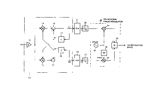
Fig. 1 is a block diagram showing an FM modulation
circuit of a first embodiment.
The FM modulation circuit comprises an input
component converting circuit 10, a first and a second
D/A converters 21 and 22, a first and a second filters
26 and 27 and a quadrature-phase modulator 30.
The input component converting circuit 10
comprising a digital signal processing circuit serves to
21~3373
- 16 -
convert an input modulation signal vn into a discrete
in-phase input signal In and a discrete quadrature-phase
input signal Qn. The input modulation signal vn is
derived from A/D converting the input modulation wave
v(t) through the A/D converter (not shown) at a sampling
cycle T. The input component converting circuit 10
comprises a coefficient circuit 11, a first and a second
delay registers 12 and 13, a first and a second
multipliers 14 and 15, an adder 16 and a subtracter 17.
o The coefficient circuit 11 multiplies the input
modulation signal vn by "a" times and outputs the signal
which has been multiplied by a constant. The value "a"
is selected to the value ~T of the equation 11. As a
result, the signal multiplied by a constant to be output
from the coefficient circuit 11 is equal to the value
~Tvn. The thus multiplied signal is supplied to the
first and the second multipliers 14 and 15.
The discrete in-phase input signal In and discrete
quadrature-phase input signal Qn output from the input
component converting circuit 10 are supplied to a first
and a second delay registers 12 and 13, respectively.
The first delay register 12 delays the discrete in-
phase input signal In by 1 sampling cycle and outputs a
delayed in-phase input signal In-l. The delayed in-phase
input signal In-l is supplied to the second multiplier 15
- 17 - 21~3373
and the adder 16.
The second delay register 13 delays the discrete
quadrature-phase input signal Qn by 1 sampling cycle and
outputs a delayed quadrature-phase input signal Qn-l. The
delayed quadrature-phase input signal Qn-l is supplied to
the first multiplier 14 and the subtracter 17.
The first multiplier 14 multiplies the multiplied
signal by the delayed quadrature-phase input signal Qn-
and outputs a first multiplication result signal, which
lo is supplied to the adder 16. The adder 16 adds the first
multiplication result signal to the delayed in-phase
input signal In-l and outputs the addition result signal
as a discrete in-phase input signal In.
The second multiplier 15 multiplies the multiplied
signal by the delayed in-phase input signal In-l and
outputs a second multiplication result signal. The
second multiplication result signal is supplied to the
subtracter 17. The subtracter 17 subtracts the second
multiplication result signal from the delayed
quadrature-phase input signal Qn-l and outputs the
subtraction result signal as the discrete quadrature-
phase input signal Qn.
The input component converting circuit 10 provides
the discrete in-phase input signal In and discrete
quadrature-phase input signal Qn of the base band of the
2ls3373
- 18 -
quadrature-phase modulator 30 by repeating recursive
processing described above.
The discrete in-phase input signal In and discrete
quadrature-phase input signal Qn are supplied to the
first and the second D/A converters 21 and 22,
respectively.
The first D/A converter 21 D/A converts the
discrete in-phase input signal In and outputs a base band
in-phase input signal I. The base band in-phase input
o signal I is subjected to the process for eliminating
unnecessary wave through the first filter 26, and then
supplied to the quadrature-phase modulator 30.
The second D/A converter 22 D/A converts the
discrete quadrature-phase input signal Qn and outputs a
base band quadrature-phase input signal Q. The base band
quadrature-phase input signal Q is subjected to the
process for eliminating unnecessary wave through the
second filter 27, and then supplied to the quadrature-
phase modulator 30.
The quadrature-phase modulator 30 comprises an
oscillator 31, a phase shifter 32, a first and a second
double-balanced mixers 33 and 34 and an adder circuit
35.
The oscillator 31 generates a base carrier (in-
phase carrier ) cos~t to be supplied to the phase
21~3373
-- 19 --
shifter 32. The phase shifter 32 delays the phase of the
in-phase carrier cos~ct by 90 and outputs the
quadrature carrier sin~ct.
The in-phase carrier cos~ct and the base band in-
phase input signal I are supplied to the first double-
balanced mixer 33.
The quadrature carrier sin~ct and the base band
quadrature-phase input signal Q are supplied to the
second double-balanced mixer 34.
lo The first double-balanced mixer 33 multiplies the
in-phase carrier cos~ct by the base band in-phase input
signal I and outputs a modulated in-phase
component signal.
The second double-balanced mixer 34 multiplies the
quadrature carrier sin~ct by the base band quadrature-
phase input signal Q and outputs a modulated quadrature
component signal.
The modulated in-phase component signal and
modulated quadrature component signal are supplied to
the adder circuit 35. The adder circuit 35 adds the
modulated quadrature component signal to the modulated
in-phase component signal and outputs an FM modulated
wave. The FM modulated wave is equivalent to the signal
derived from FM modulating the carrier cos~ct with the
input modulation signal vn.
2ls3373
- 20 -
Next, a second embodiment is described.
Fig. 2 is a block diagram of the FM modulation
circuit of the second embodiment.
The FM modulation circuit shown in Fig. 2 comprises
an input component converting circuit lOA with a circuit
for improving amplitude stability added to the input
component converting circuit 10 of the FM modulation
circuit shown in Fig. 1. The input component converting
circuit 10 shown in Fig. 1 may cause the amplitude to be
o unstable in relation with time which is influenced by
approximation executed at the equation 11, quantization
error resulted from A/D conversion, round-down error of
the multipliers, and the like. The input component
converting circuit lOA of Fig. 2 is provided with a
1~ circuit to prevent the above mentioned instability.
The input component converting circuit lOA has the
same construction as that of the input component
converting circuit 10 except a first and a second zero-
cross detection circuits 18a and 18b, a first and a
second amplitude correction circuits 19a and l9b added
thereto.
The first and the second zero-cross detection
circuits 18a and 18b comprise a first and a second data
input terminals X~, Y~ and control signal output
terminals C.
21 ~33 73
- 21 -
In the first zero-cross detection circuit 18a, the
first data input terminal Xin receives a discrete in-
phase input signal In as a first input data. The second
data input terminal Yin receives a delayed in-phase
input signal In-1 as a second input data.
In the second zero-cross detection circuit 18b, the
first data input terminal Xin receives a delayed
quadrature-phase input signal Qn-l as a first input data.
The second data input terminal Yin receives a discrete
quadrature-phase input signal Qn as a second input data.
The first zero-cross detection circuit 18a detects
the polar difference between the discrete in-phase input
signal In and the delayed input signal In-1. The second
zero-cross detection circuit 18b likewise detects the
polar difference between the discrete quadrature-phase
input signal Qn and the delayed quadrature-phase input
signal Qn-l.
Referring to Fig. 3, detailed explanation of the
first zero-cross detection circuit 18a (the second zero-
cross detection circuit 18b) is described. It is well
known that the first and the second input data have sine
bits. Each of the first and the second detection
circuits 18a and 18b is constructed with exclusive OR
gate 18-1.
The exclusive OR gate 18-1 obtains exclusive OR of
- 22 - 2 1 S 3 3 7
the sine bits of the first input data and the second
input data and outputs the resultant exclusive OR signal
from the control signal output terminal C as a zero-
cross detection signal.
With the first zero-cross detection circuit 18a, in
case the discrete in-phase input signal In has the same
polarity as that of the delayed in-phase input signal In-
, the output of the exclusive OR gate 18-1 becomes "0"
level. In case of different polarity, i.e., the discrete
0 in-phase input signal In zero crosses, the first zero-
cross detection signal at logical level "1" is output.
With the second zero-cross detection circuit 18b,
in case the discrete quadrature-phase input signal Qn has
the same polarity as that of the delayed quadrature-
phase input signal Qn-l~ the output of the exclusive OR
gate 18-1 becomes "0" level. In case of different
polarity, i.e., the discrete quadrature-phase input
signal Qn zero crosses, the second zero-cross detection
signal at logical level "1" is output.
Referring to Fig. 2 again, the first and the second
amplitude correction circuits l9a and l9b have data
input terminals in, data output terminal "out", and
control signal input terminals C, respectively.
With the first amplitude correction circuit l9a,
the data input terminal in receives the discrete in-
21~3373
- 23 -
phase input signal In as an input data signal, and the
control signal input terminal C receives the second
zero-cross detection signal, which outputs a corrected
in-phase input signal In' as output data from the data
output terminal "out".
With the second amplitude correction circuit l9b,
the data input terminal in receives the discrete
quadrature-phase input signal Qn as input data, and the
control signal input terminal C receives the zero-cross
o detection signal, which outputs a corrected quadrature-
phase input signal Qn ' as output data from the data
output terminal "out".
Upon receiving the second zero-cross detection
signal at logical level "1", i.e., when the discrete
quadrature-phase input signal Qn zero crosses, the first
amplitude correction circuit l9a outputs the in-phase
input signal In' with the same polarity as that of the
input discrete in-phase input signal In which has been
corrected to a preset amplitude value instead of the
discrete in-phase input signal In. The output is read
into the first delay register 12.
Upon receiving the first zero-cross detection
signal at logical level "1", i.e., when the discrete in-
phase input signal In zero crosses, the second amplitude
correction circuit 19b outputs the quadrature-phase
2I~3373
- 24 -
input signal Qn ' with the same polarity as that of the
input discrete quadrature-phase input signal Qn which has
been corrected to a preset amplitude value instead of
the discrete quadrature-phase input signal Qn. The output
is read into the second delay register 13.
As aforementioned, every time when the discrete in-
phase input signal In and the discrete quadrature-phase
input signal Qn zero cross, each amplitude of those
signals is corrected, thus preventing unstable variation
lo in the amplitude.
Referring to Fig. 4, a detailed explanation of the
first amplitude correction circuit l9a (the second
amplitude correction circuit 19b) is described.
The first amplitude correction circuit 19a and the
second amplitude correction circuit l9b have a first and
a second data selectors 19-1 and 19-2, respectively.
The first data selector 19-1 receives a sine bit of
the input data supplied to the data input terminal in as
a selected signal. The first data selector 19-1 also
receives both positive and negative amplitude values.
In this invention, the positive amplitude value is
set to +1, and the negative amplitude value is set to -
1. If the sine bit of the input data is positive, i.e.,
at logical level "0", the first data selector 19-1
selects the positive amplitude value +1 as a selected
~1~3373
- 25 -
value. While if the sine bit of the input data is
negative, i.e., at logical level "1", the first data
selector 19-1 selects the negative amplitude value -1 as
a selected value.
The selected amplitude value is supplied to one
input terminal of the second data selector 19-2 to which
a zero-cross detection signal is supplied as a selected
signal.
If the zero-cross detection signal is at logical
o level "0", i.e., zero-cross is not detected, the second
data selector 19-2 outputs the input data (discrete in-
phase input signal In or discrete quadrature-phase input
signal Qn) ~ as is, supplied from the data input terminal
in as output data (corrected in-phase input signal In'
or quadrature-phase input signal Qnl) from a data output
terminal "out".
If the zero-cross detection signal is at logical
level "1", i.e., zero-cross is detected, the second data
selector 19-2 outputs the selected amplitude value
supplied from the first data selector 19-1 as output
data from the data output terminal "out".
It is further understood that the form of the
invention shown and described is to be taken as
preferred embodiments thereof and that various changes
may be resorted to without departing from the spirit of
21~3373
- 26 -
the invention or the scope of the claims. For example,
various systems other than that shown in Fig. 4 may be
available for the amplitude correction means.