Note: Descriptions are shown in the official language in which they were submitted.
215351~
~.
MOBILE STATION FOR CDMA MOBILE COMMUNICATION SYSTEM
AND
DETECTION METHOD OF THE SAME
BACKGROUND OF THE INVENTION
Field of the Invention
The present invention relates to a mobile
communication system, and more particularly to a mobile
station for a CDMA (Code Division Multiple Access) mobile
communication system which uses pilot signals inserted in
a forward link for data demodulation, and a detection
method to be used at the mobile station.
Description of the Related Art
A coherent detection method using a PLL (Phase
Locked Loop) circuit and a differential detection method
are known as conventional detection (demodulation)
methods.
With the coherent detection method, shifts of
a carrier fre~uency and phase in a carrier band between
transceivers are compensated by a PLL circuit at a re-
ceiver side. In a mobile communication system incorpo-
rating a coherent detection method, a PLL circuit cannot
follow the state (dynamic characteristics) when fading or
the like is generated because of a moving mobile station,
and there is a problem of a considerably degraded error
rate performance.
With the differential detection method on the
other hand, data is converted into phase differences of
a transmission signal by differential coding, and
2153516
transmitted from a transmitter. At a receiver, data is
demodulated by differential coding without obtaining the
absolute phase of data. With this method, although it is
not necessary to make the frequency and absolute phase
coincide both at the receiver and transmitter, the error
rate performance is degraded even at the state (static
characteristics) when a mobile station is at a stand-
still.
As one of the detection methods ensuring that
the error rate performance is not degraded in both the
dynamic and static characteristics, a data demodulation
method has been proposed which uses pilot signals insert-
ed in a forward link (channel), as described, for exam-
ple, in "A study on Demodulation Method for CDMA Mobile
Phone", by Hideshi MURAI et al., Spring Symposium of 1994
of the Institute of Electronics, Information and Communi-
cation Engineers, A-5 Spread Spectrum, A-268, p. 1 - 270
(1994)-
Fig. 2 illustrates the procedure of signal
modulation/demodulation at a base station 51 and a mobilestation 52 in a conventional CDMA mobile communication
system using pilot signals inserted in a forward link.
The base station 51 converts a transmission
signal (data signal) to each mobile station 52 into two
series of data signals (I, Q) 50 by a serial-parallel
converter or coding circuit, and supplies the data sig-
nals I and Q to respective multipliers 501A and 501B to
spread them by using spreading codes (PNID, PNQD)) 54 for
2153~16
data symbol.
For example, as the spreading codes, codes of
a 128-chip length having a symbol rate 128 times faster
than that of the data signals. Each code (bit "1" or
"0") of transmission data is converted into a code pat-
tern made of 128 chips and into a phase inverted code
pattern.
The data signals I and Q spread by the spread-
ing codes 54 are quadrature-multiplexed at the multipli-
ers 502A and 502B, for example, by QPSK (Quadrature PhaseShift Keying), thereafter added together by an adder 503,
and transmitted from an antenna in the form of radio
waves in a radio frequency band 55. Fig.lOA shows a
relationship between the combinations of the values ("1"
and "0") of the signals I and Q and the signal constella-
tion by QPSK.
In order to communicate with a plurality of
mobile stations, the base station assigns a spreading
code for data symbol specific to each mobile station to
form a plurality of signal channels. For example, at a
channel X, the data signals I(X) and Q(X) are spread by
spreading codes PNID(X) and PNQD(X) specific to the
channel (X), whereas at a channel Y, the data signals
I(Y) and Q(Y) are spread by spreading codes PNID(Y) and
PNQD(Y) specific to the channel (Y).
In addition to data signals for a plurality of
channels, the base station 51 transmits pilot signals
which are used as a reference signal at each mobile
215351~
station 52 for the demodulation of data signals. For the
pilot signals, two series of signals I(P) and Q(P) having
a fixed bit pattern (continuous pattern of bits "1") are
spread by spreading codes PNIp and PN_Qp specific to each
pilot signal channel having a chip pattern different from
that of the spreading codes 54 for data symbol,
quadrature-multiplexed in the manner similar to data
signals, and transmitted as radio waves in the radio
frequency band 55 same as that of data signals.
Fig. 2 shows a quadrature multiplexing circuit
only for a single channel for the simplicity of the
drawing. In an actual CDMA transmission circuit, signals
of a plurality of channels (data signal channels and
pilot signal channels) spectrum-spread by specific
spreading codes are multiplexed for each of the I and Q
signal components, and supplied to the multipliers 502A
and 502B for quadrature multiplexing.
At each mobile station 52, signals received by
the antenna are supplied to multipliers 504A and 504B to
quadrature-detect them by signals having a local oscilla-
tion frequency and generated by an oscillator 520.
Output signals from this detection circuit are supplied
to LPFs (Low Pass Filters) 56A and 56B to eliminate high
frequency components and obtain reception signals (I',
Q') 1.
Since an oscillator 510 for quadrature
multiplexing at the base station and the quadrature
detection (demodulation) oscillator 520 at each mobile
2153516
station operate asynchronously, the detected reception
signals (I', Q') 1 contain signal value errors caused by
a phase shift (or frequency shift) from the phase (fre-
quency) at the modulation side. The quadrature detection
by the oscillator 520 is tentative so that the reception
signals (I', P') 1 are required to be subjected to signal
processing for eliminating phase errors (hereinafter
called phase correction).
Fig. 3 shows the structure of a conventional
mobile station detection circuit for removing signal
value errors caused by the phase shift, from the recep-
tion signals (I', P') 1, and for regenerating the data
signals (I, Q) same as that transmitted from the base
station.
A pilot signal despreading circuit 21
despreads the reception signals 1 by using spreading
codes 26 for pilot symbol, and generates phase error
signals (hcos~, ~sin~) 22 changing with a phase shift
angle. An averaging circuit 23 averages the phase error
signals (~cos~, ~sin~) 22 outputted from the despreading
circuit 21, for a period of a plurality of chips, and
generates correction signals (~COS~, hSIN~) 24 which are
supplied to a phase correction circuit 30. A spreading
code generation circuit 25 generates spreading codes (PN
IP~ PNQp) for pilot symbol to be supplied to the pilot
signal despreading circuit 21 and spreading codes (PN~D,
PNQD) for data symbol to be supplied to a data signal
despreading circuit 32 to be described layer. The
2t~3516
.
spreading codes (PN~D, PNQD) for data symbol have a code
pattern specific to each signal channel.
A delay circuit 28 delays the reception sig-
nals 1 by a time duration corresponding to the time
required for the averaging circuit 23 to perform an
averaging process for the phase error signals (~cos~,
~sin~). The phase correction circuit 30 corrects the
phases of signals 29 outputted from the delay circuit 28.
A data signal despreading circuit 32 despreads phase-
corrected signals 31 by spreading codes 27 for data
symbol. Accumulators 34 convert data signals 33
outputted from the despreading circuit 32 and having the
chip rate into demodulated data (I, Q) having the symbol
rate of the transmission signal.
Referring to Fig. lOB, a relation between a
transmission signal from the base station and a reception
signal 1 at a mobile station will be described, while
paying attention to a pilot signal whose signals (I, Q)
are always transmitted as values (1, 1).
A pilot signal Pl transmitted at the base
station with a value (I = 1, Q = 1) at the first sector
in the I-Q signal constellation changes to a signal
having a value (I = i', Q = q') at the mobile station in
the I'-Q' signal constellation, assuming that the phase
shift angle is ~. If the phase shift angle ~ is greater
than ~/2, the pilot signal Pl is received at the mobile
station as a signal in a different sector (second to
fourth sectors) in the I'- Q' signal constellation, and
215~16
takes a value quite different from the transmission
signal at the base station.
On the assumption that the pilot signal Pl has
essentially a value of i = q in the first sector in the
I'-Q' signal constellation as indicated by a point P2,
the phase shift amount (angle ~) between the I'-Q' signal
constellation and the I-Q signal constellation is detect-
ed from the values of I and Q components of the received
pilot signal.
Referring back to Fig. 3, the pilot signal
despreading circuit 21 despreads the received signals
(I', Q') 1 by using the spreading codes 26 for pilot
symbol. Of the reception signals 1, the signal compo-
nents I' are inputted to multipliers 210A and 211A,
whereas the signal components Q' are inputted to multi-
pliers 210B and 211B. PNIp of the spreading code 26 for
pilot symbol of the I components is supplied to the
multipliers 210A and 210B, whereas PNQp of the spreading
code 26 for pilot symbol of the P components is supplied
to the multipliers 211A and 211B. Outputs of the multi-
pliers 210A and 211B are added together by an adder 212A,
whereas outputs of the multipliers 210B and 211AB are
subtracted by a subtractor 212B.
Because of the above-described phase shift,
both the reception signals I' and Q' contain both the I
and Q components of the transmission pilot signals. At
the pilot signal despreading circuit 21, the reception
signal I' is despread by the spreading codes PNIp and PN
21535~6
Qp to obtain the Ii and Iq components of the pilot sig-
nal, whereas the reception signal Q' is despread by the
spreading codes PNIp and PNQp to obtain the Qi and Qq
components of the pilot signal. Furthermore, the Ii and
Qq components are added together by the adder 212A to
obtain the phase error signal ~cos~ proportional to COS~,
whereas the Qi components are subtracted by the Iq compo-
nents by the subtractor 212B to obtain the phase error
signal hsin~ proportional to SIN~.
The averaging circuit 23 averages the phase
error signals (~cos~, ~sin~) 22 outputted from the
despreading circuit 21 for a period of a plurality of
chips, and generates phase correction signals (~COS~,
~SIN~) 24 with noises being eliminated.
The averaging circuit 23 is constituted by,
for example as shown in Fig. 4, two analog value shift
registers (serial to parallel converters) and two adders
235 and 236. The two shift registers are constituted by
a plurality of one-chip delay gates (Dc) 230 connected in
series for shifting the phase error signals ~cos~ and
~sin~. The adders 235 and 236 add the output signals
from the respective delay gates 230.
A delay gate Ds corresponding to one symbol is
formed by serially connected one hundred and twenty eight
one-chip delay gates (Dc) 230. In this example, each
shift register is constituted by serially connected three
symbol delay gates 231, 232, and 233, and the values of
the phase error signals hcos~ and ~sin~ corresponding to
215351~
the 128 x 3 chips continuous on a time axis are added
together by the adders 235 and 236 to thereby obtain the
phase correction signals ~COS~ and ~SIN~ with noises
being eliminated through averaging.
The delay circuit 28 is constituted by, for
example as shown in Fig. 5, two analog value shift regis-
ters (delay circuit) each formed by a plurality of seri-
ally connected one-chip delay gates Dc 280. The number N
of delay chips required for the averaging circuit 23 (in
this example, N = 128 x 3) and the number M of delay
chips required for the delay circuit 28 satisfy the
condition of M = (N-1)/2.
This condition is set because the phase errors
of the received data signals are corrected by the phase
correction values obtained by a set of pilot signals
extending before and after the received data signals by a
predetermined number of chips.
In this example, M = 191.5. Therefore, the
number M of delay chips is set to "191" or "192". Ds 281
is a delay gate unit corresponding to one symbol having
one hundred and twenty eight one-chip delay gates Dc 280.
In order to set the total number of delay chips to "191"
or "192", the delay gate unit 281 is connected to a half
symbol delay unit Ds' 282 which is constituted by sixty
three or sixty four one-chip delay gates Dc 280.
In the phase correction circuit 30, for exam-
ple as shown in Fig. 6, the I' and Q' components of delay
data 29 outputted from the delay circuit 28 are
~ 2 ~ 5 3 5 ~ 6
~,~
.~,.
- 10 -
multiplied respectively by the correction signals 24 of COS~
and SIN~ by multipliers 301A, 301B, 302A, and 302B, and
addition and subtraction are performed by an adder 303A and
a subtractor 303B to correct the errors of the received data
5 signal values caused by the phase shift. In this manner,
the data despreading circuit 32 can demodulate received data
signals (I, Q) 35.
As described above, in the detection circuit of a
conventional CDMA mobile communication system, an averaging
10 process of phase errors detected from pilot signals and a
delay and phase correction process of received data signals
are both performed at a chip rate of spreading codes.
Therefore, the circuit portions for performing these
processes are required to be operated synchronously with
15 high speed clocks, so that the constituent components of the
detection circuit become expensive and a power consumption
becomes large.
SUMMARY OF THE INVENTION
It is an object of the present invention to
20 provide a mobile station of a CDMA mobile communication
system and a detection method used at the mobile station,
capable of performing a phase correction process by using
low speed clocks and lowering a power consumption.
In accordance with one aspect of the present
25 invention there is provided a mobile station of a code
division multiple access mobile communication system wherein
a base station multiplexes through spectrum-spread a pilot
signal and a data signal having I and Q components by using
specific spreading signals, and quadrature multiplexes for
transmission, the mobile station comprising: a quadrature
.~.
- lOa -
detection circuit for separating a reception signal into an
I component multiplexed signal and a Q component multiplexed
- signal; a first despreading circuit for generating first and
second phase error signals having values corresponding to
phase shifts between the quadrature detection circuit and a
quadrature multiplexer of the base station, by despreading
the I component multiplexed signal and the Q component
multiplexed signal by using first spreading codes for pilot
symbol specific to I and Q components; a circuit for
generating first and second phase correction signals having
a symbol rate of the data signal, by processing the first
and second phase error signals supplied from said first
despreading circuit; a second despreading circuit for
outputting a data signal group, by despreading the I and Q
component multiplexed signals by using second spreading
codes specific to I and Q components of respective data
reception channels; a rate conversion circuit for converting
the transmission rate of the data signal group outputted
from said second despreading circuit into the symbol rate of
the data signal; and a phase correction circuit for
generating the I and Q component data signals for decoding
by correcting the value of each data signal of the data
signal group of the converted symbol rate in accordance with
the first and second phase correction signals.
In accordance with another aspect of the present
invention there is provided a mobile station of a code
division multiple access mobile communication system wherein
a base station multiplexes through spectrum-spread a pilot
signal and a data signal having I and Q components by using
specific spreading signals, and quadrature multiplexes for
transmission, the mobile station comprising: a quadrature
,.~
~21535 ~6
. .,
- lOb -
detection circuit for separating a reception signal into an
I component multiplexed signal and a Q component multiplexed
- signal; a first despreading circuit for generating first and
second phase error signals having values corresponding to
phase shifts between the quadrature detection circuit and a
quadrature multiplexer of the base station, by despreading
the I component multiplexed signal and the Q component
multiplexed signal by using first spreading codes for pilot
symbol specific to I and Q components; a first rate
conversion circuit for converting the transmission rate of
the first and second phase error signals supplied from said
first despreading circuit into the symbol rate of the data
signal; a second despreading circuit for outputting a data
signal group, by despreading the I and Q component
multiplexed signals by using second spreading codes specific
to I and Q components of respective data reception channels;
a second rate conversion circuit for converting the
transmission rate of the data signal group outputted from
said second despreading circuit into the symbol rate of the
data signal; and a signal processing unit for generating the
I and Q component data signals for decoding by correcting
the value of each data signal of the data signal group
supplied from said second rate conversion circuit in
accordance with the first and second phase correction
signals of the symbol rate supplied from said first rate
conversion circuit.
In accordance with yet another aspect of the
present invention there is provided a detection method for a
mobile station of a code division multiple access mobile
communication system wherein a base station multiplexes
-- through spectrum-spread a pilot signal and a data signal,
! ~l
,~ .,
4~ ~
',_
- lOc -
and quadrature multiplexes for transmission from the base
station to the mobile station, comprising the steps of:
separating through quadrature detection a reception signal
into an I component multiplexed signal and a Q component
multiplexed signal; generating first and second phase error
signals by despreading the I component multiplexed signal
and the Q component multiplexed signal by using first
spreading codes for pilot symbol specific to I and Q
components; generating a data signal group by despreading
the I and Q component signals by using second spreading
codes specific to I and Q components of respective reception
data channels; generating first and second phase correction
signals having a symbol rate of the data signal, by
processing the first and second phase error signals;
converting the transmission rate of the data signal group
into the symbol rate of the data signal; and generating the
I and Q component data signals for decoding by correcting
the value of each data signal of the data signal group of
the converted symbol rate in accordance with the first and
second phase correction signals.
In an embodiment of the present invention the
phase correction signals (COS~, SIN~) are obtained by
serial-to-parallel converting phase error signals (~cos~,
~sin~) converted to have a symbol rate by using relatively
low speed shift registers operating at the symbol rate, and
by averaging the phase error signals for a plurality of
symbols by using adders.
In a conventional mobile station, after the
phases of the reception signals are corrected, the reception
signals are despread by using despreading codes for data
~ symbol to extract the I and Q components of the reception
!~2~535 16
data signals. According to the present invention, after the
I and Q components of the reception signals obtained by
quadrature detection are despread by the data signal
despreading circuit, the transmission rate of the data
signal group outputted from the data signal despreading
circuit is changed to the symbol rate, and the data signal
group is inputted via a delay circuit to a phase correction
circuit.
With the above structure of this invention, the
process of averaging phase error signals, data signal delay
process, and data signal phase correction process can be
performed at the symbol rate. Therefore, the circuit
portions for these processes can be operated at
~153516
- 12 -
low speed clocks and a power consumption can be reduced.
BRIEF DESCRIPTION OF THE DRAWINGS
Fig. 1 is a block diagram of a detection
circuit of a mobile station of a CDMA mobile communica-
tion system according to an embodiment of the invention.
Fig. 2 is a diagram showing a quadraturemultiplexing circuit of a base station and a quadrature
detection circuit of a mobile station.
Fig. 3 is a block diagram showing an example
of a conventional detection circuit of a mobile station
of a CDMA mobile communication system.
Fig. 4 shows the structure of a conventional
averaging circuit 23 for phase error signals.
Fig. 5 shows the structure of a conventional
delay circuit 28.
Fig. 6 shows the structure of a conventional
phase correction circuit 30.
Fig. 7 shows the structure of an averaging
circuit 43 for phase error signals according to the
present invention.
Fig. 8 is a diagram showing an example of the
structure of a delay circuit 48 according to the present
invention.
Fig. 9 is a diagram showing an example of the
structure of a phase correction circuit according to the
present invention.
Fig. lOA is a diagram showing a signal
~2~535 ~6
- 13 -
constellation of QPSK.
Fig. lOB is a diagram illustrating phase er-
rors.
DESCRIPTION OF THE PREFERRED EMBODIMENTS
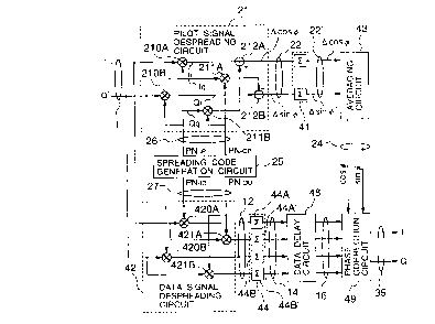
Fig. 1 is a block diagram showing the struc-
ture of a detection circuit for a CDMA mobile communica-
tion system according to the present invention. In order
to make it easy to compare with the conventional system
shown in Fig. 3, circuit elements similar to those shown
in Fig. 3 are represented by using the identical refer-
ence numerals in Fig. 1.
In Fig. 1, a pilot signal despreading circuit
21 despreads the quadrature multiplexed reception signals
1 by using spreading codes for pilot symbol and generates
phase error signals (hcos~, hsin~) 22 changing with a
phase shift angle. Accumulators 41 convert the phase
error signals outputted from the pilot signal despreading
circuit 21 at a chip rate into signals (hcos~l, hsin~l)
22' of a symbol rate. An averaging circuit 43 averages
the phase error signals (hcos~', hsin~') for a period of
a plurality of symbols, and generates phase correction
signals. A spreading code generation circuit 25 gener-
ates spreading codes 26 (PNIp, PNQp) for pilot symbol and
spreading codes 27 (PNID, PNQD) for data symbol. A data
signal despreading circuit 42 despreads the reception
signals by using the spreading codes 27 for data symbol.
Accumulators 44 convert the transmission rate of the data
- 14 -
signals 12 despread by the data signal despreading cir-
cuit 42, from the chip rate into the symbol rate. A data
delay circuit 48 delays the reception signals 14 of the
symbol rate by a time duration corresponding to the time
required for the averaging circuit 43 to perform an
averaging process for the phase error signals. A phase
correction circuit 49 corrects the phases of reception
signals outputted from the data delay circuit 48 by phase
correction signals 24. Reference numeral 35 represents phase
corrected and demodulated data (I, Q).
The pilot signal despreading circuit 21
despreads the reception signals (I', Q') 1 by using the
spreading codes 26 (PNIp, PNQp) for pilot symbol. In
this case, both the reception signals I' and Q' are
despread at multipliers 210A to 211B by using the I and Q
components (PNIp, PNQp) of the despreading codes 26 for
pilot symbol, and thereafter as shown in Fig. 1, addition
and subtraction are performed by an adder 212A and a
subtractor 212B to thereby obtain the values (phase
errors) ~cos~ and ~sin~ proportional to the phase error
angle ~. The phase error signals 22 outputted from the
pilot signal despreading circuit 21 at the chip rate are
integrated by the accumulators 41 for each symbol period
(128-chip period) to thereby convert them into the phase
25 error signals (~cos~' and ~sin~') 22' which are then
supplied to the averaging circuit 43.
~"~
~ 2~53516
A 15
- The averaging circuit 43 averages the phase
error signals (~cos~ sin~') 22' inputted in a period
of a plurality of symbols, and generates phase correction
signals (COS~, SIN~) 24 for the reception data. An
example of the structure of the averaging circuit 43 is
shown in Fig. 7.
Ds 430 represents an analog gate having a one-
symbol delay time. In this example, in order to elimi-
nate noises from the phase error signals ~cos~' and
~sin~', the phase error signals ~cos~' and ~sin~' of the
symbol rate are inputted to shift registers SR-A and SR-B
each constituted by two-stage symbol delay gates 430.
Two sets of the phase error signals of three symbols
including an input signal to the shift register and
output signals from the delay gates are added together by
adders 431 and 432. The adders 431 and 432 multiply the
addition results by proper coefficients to average the
phase error signals ~cos~' and ~sin~' and to output the
results as the phase correction signals COS~ and
SIN~. The shift registers SR-A and SR-B are not neces-
sary to be-formed by a number of chip delay gates operat-
ing at a high speed chip rate as with the conventional
technique illustrated in Fig.4, but are formed by delay
gates operating at a low speed symbol rate.
At the data signal despreading circuit 42, the
reception signal I' is supplied to multipliers 420A and
421A, whereas the reception signal Q' is supplied to
multipliers 420B and 421B. Four series of despread data
21~351~
- 16 -
signals 12 are obtained by supplying the spreading code
PNID to the multipliers 420A and 420B and by supplying
the spreading code PNQD to the multipliers 421A and 421B.
The transmission rate of these despread data signals 12
is converted from the chip rate into the symbol rate by
four accumulators 44 (44A to 44B') provided in correspon-
dence with the four multipliers 420A to 421B. Data
signals 14 of the symbol rate are delayed by the data
delay circuit 48 by a predetermined time determined by a
time required for the averaging circuit 43 to perform an
averaging operation.
An example of the data delay circuit 48 is
shown in Fig. 8. The number N of symbols required for
averaging the phase error signals and the number M of ~
delay chips required for the data delay circuit 48 satis-
fy the condition of M = (N-1)/2. As shown in Fig. 7, the
averaging circuit 43 uses two-symbol shift registers (N =
2) so that the number M of delay symbols necessary for
the data delay circuit 48 is one. In this case, as shown
in Fig. 8, the data delay circuit 48 delays the outputs
of the accumulators by one-stage symbol delay gates Ds
480 (480A to 480B') each operating at the symbol rate.
The phase correction circuit 49 corrects the
values of the data signals 16 outputted from the data
delay circuit 48 at the symbol rate by using the phase
correction signals 24 to thereby obtain the data signals
I and Q with the influence of the phase errors being
removed.
~21535~6
- 17 -
An example of the structure of the phase
correction circuit 49 is shown in Fig. 9. Of the delayed
data signals, the I component signal is multiplied by the
phase correction signal COS~ at multipliers 490A and
490A', whereas the Q component signal is multiplied by
the phase correction signal SIN~ at multipliers 490B and
490B'. The multiplication results are subjected to
addition and subtraction by an adder 491A and a
subtractor 491B as shown in Fig. 9 to thereby obtain
phase corrected data signals (I, Q) 35. By processing
these data signals 35 by a decoding circuit (not shown),
it is possible to demodulate data signals transmitted
from the base station.
In the above embodiment, the pulse trains 12
and 22 obtained by despreading the reception signals by
using the despreading codes for pilot symbol and data
symbol, are converted into pulse trains of the symbol
rate which are then subjected to phase correction. It is
therefore possible to lower the clock rate of the circuit
for correcting phase errors.
In the above embodiment, the phase error
signals are averaged by three symbols. If the number of
symbols to be averaged is five, seven, or nine, the
number of delay gates of the data delay circuit is set to
two, three, or four. In the circuit arrangement shown in
Fig. 1, the functions of the averaging circuit 43, data
delay circuit 48, and phase correction circuit 49 may be
realized by software using a digital signal processor.
2153516
In this case, a digital signal processor processes the
input signals at the symbol rate so that the number of
program executions for phase correction can be reduced
considerably.