Note: Descriptions are shown in the official language in which they were submitted.
- 2153554
CFO 10771 CA
APPARATUS FOR MANUFACTURING ELECTRON
SOURCE AND IMAGE FORMING APPARATUS
BACKGROUND OF THE INVENTION
Field of the Invention
This invention relates to an apparatus for
manufacturing an electron source and an image forming
apparatus.
Related Backqround Art
There have been known two types of electron-
emitting device; the thermoelectron emission type and
the cold cathode electron emission type. Of these, the
cold cathode emission type refers to devices including
field emission type (hereinafter referred to as the FE
type) devices, metal/insulation layer/metal type
(hereinafter referred to as the MIN type) electron-
emitting devices and surface conduction electron-
emitting devices. Examples of FE type device include
those proposed by W. P. Dyke & W. W. Dolan, "Field
emission", Advance in Electron Physics, 8, 89 (1956)
and C. A. Spindt, "PHYSICAL Properties of thin-film
field emission cathodes with molybdenum cones", J.
Appl. Phys., 47, 5284 (1976).
Examples of MIN device are disclosed in papers
including C. A. Mead, "The tunnel-emission amplifier",
J. Appl. Phys., 32, 646 (1961).
Examples of surface conduction electron-
21~35~4
- 2 -
emitting device include one proposed by M. I. Elinson,
Radio Eng. Electron Phys., 10 (1965).
A surface conduction electron-emitting device
is realized by utilizing the phenomenon that electrons
are emitted out of a small thin film formed on a
substrate when an electric current is forced to flow
in parallel with the film surface. While Elinson
proposes the use of SnO2 thin film for a device of
this type, the use of Au thin film is proposed in [G.
Dittmer: "Thin Solid Films", 9, 317 (1972)] whereas
the use of In203/SnO2 and that of carbon thin film
are discussed respectively in [M. Hartwell and C. G.
Fonstad: "IEEE Trans. ED Conf.", 519 (1975)] and [H.
Araki et al.: "Vacuum", Vol. 26, No. 1, p. 22 (1983)].
Fig. 34 of the accompanying drawings
schematically illustrates a typical surface conduction
electron-emitting device proposed by M. Hartwell.
In Fig. 26, reference numeral 1 denotes a substrate.
Reference numeral 4 denotes an electroconductive thin
film normally prepared by producing an H-shaped thin
metal oxide film by means of sputtering, part of which
eventually makes an electron-emitting region 5 when
it is subjected to an electrically energizing process
referred to as "energization forming" as described
hereinafter. In Fig. 26, the thin horizontal area
of the metal oxide film separating a pair of device
electrodes has a length L of 0.5 to 1 [mm] and a width
~ - 3 - 21535S4
W of 0.1 [mm].
It should be noted, however, that a surface
conduction electron-emitting device does not
necessarily have a H-shaped film prepared in a single
operation. Alternatively, a pair of electrodes may be
arranged in parallel with each other like the pillars
of H in the first place and thereafter an
electroconductive thin film may be formed to link
the electrodes. The material and the thickness of
the thin film may be different from those of the
electrodes.
Conventionally, an electron emitting region 5
is produced in a surface conduction electron-emitting
device by subjecting the electroconductive thin film 4
of the device to an electrically energizing preliminary
process, which is referred to as "energization
forming". In the energization forming process, a
constant DC voltage or a slowly rising DC voltage that
rises typically at a rate of 1 V/min. is applied to
given opposite ends of the electroconductive thin film
4 to partly destroy, deform or transform the film and
produce an electron-emitting region 5 which is
electrically highly resistive. Thus, the electron-
emitting region 5 is part of the electroconductive
thin film 4 that typically contains a gap or gaps
therein so that electrons may be emitted from the gap.
Note that, once subjected to an energization forming
~ _ 4 _ 215 3 5 5 4
process, a surface conduction electron-emitting device
comes to emit electrons from its electron emitting
region 5 whenever an appropriate voltage is applied
to the electroconductive thin film 4 to make an
electric current run through the device.
Since a surface conduction electron-emitting
device has a particularly simple structure and can be
manufactured in a simple manner, a large number of such
devices can advantageously be arranged on a large area
without difficulty. As a matter of fact, a number of
studies have been made to fully exploit this advantage
of surface conduction electron-emitting devices.
For example, there have been proposed various types of
image forming apparatus including a self-emission type
flat image forming apparatus.
In a typical example of electron source
comprising a large number of surface conduction
electron-emitting devices, the devices may be arranged
in parallel rows and the positive and negative
electrodes of the devices of each row may be connected
to respective common wirings (ladder arrangement) as
shown in Fig. 14 or a matrix of wirings may be formed
and the devices may be connected to the respective
wirings as shown in Fig. 10.
In order for an image forming apparatus
comprising a number of electron-emitting devices to
stably provide clear and bright images, the devices
2153554
- 5 -
are required to operate uniformly and efficiently
for electron emission. The efficiency of a surface
conduction electron-emitting device is defined by the
ratio of the electric current flowing between the
paired electrodes of the device (hereinafter referred
to "device current") to the electric current produced
by electrons emitted into the vacuum of the image
forming apparatus (hereinafter referred to as "electron
emission current") when a certain voltage is applied
to the device electrodes. If all the electron-emitting
devices of the electron source operate uniformly and
efficiently for electron emission in, for instance, an
image forming apparatus comprising a fluorescent body
as its image forming member, such an apparatus can make
a high definition image forming apparatus or television
set that can be very flat and consumes power only at a
reduced rate. By turn, the drive circuit and other
components of such an energy saving apparatus may be
manufactured at low cost.
SU~qARY OF THE INVENTION
As a result of intensive research efforts, the
inventors of the present invention discovered that, if
a certain voltage is applied to a surface conduction
electron-emitting device in an atmosphere that contains
organic substances after producing an electron emitting
region therein by energization forming as described
21535~
- 6 -
above, the electric current brought into being by
electrons emitted from that region remarkably
increases. This operation is termed "activation".
The above phenomenon is attributable to an activated
filmy deposit of carbon or a carbon compound produced
in the vicinity of the electron emitting region as a
result of the voltage application.
When an electron source as shown in Fig. 14 or
Fig. 10 is subjected to an activation process, a pulse
voltage may be applied simultaneously to all the
devices of a same row or sequentially to the devices of
a same row on a one by one basis to form a filmy
deposit of an activated substance one each device.
However, with the above described technique of
activation, where a pulse voltage is applied for a
predetermined period of time under given conditions,
the electron-emitting devices can show different
extends of activation probably as a function of minute
differences in the manufacturing conditions of the
devices such as deviations in the film thickness of the
electroconductive thin film and differences in the
partial pressures of the organic substances in the
manufacturing environment depending on the relative
positions of the devices. Then, the net result will
be that the devices of the electron source do not
operate uniformly and the distribution of brightness
of the image forming apparatus shows an remarkable
21S~554
- 7 -
unevenness. While these problems may be solved to some
extent by correcting the operation of each device when
it is driven, such a corrective measure will require a
large memory device for storing corrective information
for each device and, consequently, the image forming
apparatus comprising a large number of electron-
emitting devices will inevitably become large and
costly.
Additionally, an activated filmy deposit can
be formed in unnecessary areas of the electron-emitting
device to electrically connect the positive and
negative electrodes during the activation process.
Then, an electric current (leak current) that is not
good for electron emission may flow between the
electrodes to reduce the efficiency of electron
emission and raise the rate of power consumption of
the device. Then, the device may generate heat in the
inside of the electron source so that the latter may
have to be provided with a heat radiation mechanism for
discharging the heat accumulated in the inside, which
by turn may require a power consuming drive circuit.
All in all, these and other negative factors can
severely restrict the design of the image forming
apparatus. While such factors may be prevented from
entering the scene by completing the activation process
before the route for the leak current grows remarkably
and carrying out an additional operation of
21~554
- 8 -
stabilization for removing any possible route of
leak current, then the activation process has to be
terminated before the device is processed to allow
a sufficiently large electron emission current Ie.
In view of the above described technological
problems, it is an object of the present invention to
provide an apparatus for manufacturing an electron
source that operates uniformly for electron emission
with a low power consumption rate and an image forming
apparatus having such an electron source.
According to an aspect of the invention, there
is provided a method of manufacturing an electron-
emitting device having a pair of device electrodes and
an electroconductive thin film including an electron
emitting region arranged between the electrodes,
characterized in that it comprises an activation
process for increasing the emission current of the
device and said activation process includes steps of
a) applying a voltage (Vact) to the electroconductive
thin film having a gap section under initial
conditions, b) detecting the electric performance
of said electroconductive thin film and c) modifying,
if necessary, said initial conditions as a function
of the detected electric performance of the
electroconductive thin film.
According to another aspect of the invention,
there is provided an apparatus for carrying out an
9 21~3~5 4
activation process on an electron-emitting device
having a pair of device electrodes and an
electroconductive thin film including an electron
emitting region arranged between the electrodes in
order to increase the emission current of the device,
characterized in that it comprises a) means for
applying a voltage (Vact) to the electroconductive
thin film having a gap section under initial
conditions, b) means for detecting the electric
performance of said electroconductive thin film and
c) means for modifying, if necessary, said initial
conditions as a function of the detected electric
performance of the electroconductive thin film.
BRIEF DESCRIPTION OF THE DRAWINGS
Fig. lA is a block diagram of a manufacturing
apparatus according to the invention, showing a
possible configuration thereof.
Fig. lB is a block diagram of a manufacturing
apparatus according to the invention, showing another
possible configuration thereof.
Fig. 2 is a flow chart, illustrating a
manufacturing method according to the invention.
Figs. 3A and 3B are schematic views of a
surface conduction electron-emitting device, to
which the present invention is applicable.
Fig. 4 is a schematic view of another
` lo- 21~3~4
surface conduction electron-emitting device, to
which the present invention is applicable.
Figs. 5A through 5C are schematic views of
still another surface conduction electron-emitting
device, illustrating different steps of manufacturing
it, to which the present invention is applicable.
Figs. 6A and 6B are graphs showing pulse
voltage waveforms that can be used for the energization
forming process of manufacturing a surface conduction
electron-emitting device.
Figs. 7A and 7B are graphs showing pulse
voltage waveforms that can be used for the activation
process of manufacturing a surface conduction electron-
emitting device.
Fig. 8 is a block diagram of a gauging system
for determining the electron emitting performance of
a surface conduction electron-emitting device or an
electron source.
Fig. 9 is a graph showing the relationship
between the device voltage and the device current as
well as the relationship between the device voltage
and the emission current of a surface conduction
electron-emitting device or an electron source.
Fig. 10 is a schematic partial plan view of
an electron source of matrix arrangement.
Fig. 11 is a partial cut away schematic
perspective view of an image forming apparatus
11 - 21S~55 4
comprising an electron source of matrix arrangement.
Figs. 12A and 12B are schematic views,
illustrating two possible configurations of fluorescent
film that can be used for the purpose of the present
invention.
Fig. 13 is a block diagram of a drive circuit
of an image forming apparatus, to which the present
invention is applicable.
Fig. 14 is a schematic plan view of an electron
source of ladder arrangement.
Fig. 15 is a partially cut away schematic
perspective view of an image forming apparatus
comprising an electron source of ladder arrangement.
Fig. 16A is a block diagram of a manufacturing
apparatus according to the invention, showing still
another possible configuration thereof.
Fig. 16B is a block diagram of a manufacturing
apparatus according to the invention, showing a further
possible configuration thereof.
Fig. 17 is a schematic plan view of serially
arranged surface conduction electron-emitting devices,
to which the present invention is applicable.
Figs. 18A and 18B are graphs, illustrating
pulse voltage waveforms that can be used for the
activation process of a manufacturing apparatus and
a manufacturing method according to the invention.
Figs. l9A through l9H are schematic partial
21S3~54
- 12 -
views of an electron source, illustrating a method of
manufacturing the same, to which the present invention
is applicable.
Fig. 20 is a schematic plan view of an electron
source of matrix arrangement, illustrating the wiring
for conducting an energization forming process.
Fig. 21 is a schematic block diagram of the
means for applying an activation pulse voltage in
Example 13.
Fig. 22 is a schematic diagram for illustrating
the operation of a line selecting section in Example
13.
Fig. 23 is a timing chart for illustrating the
relationship between pulse generation and the operation
of a line selecting section in Example 13.
Fig. 24 is a timing chart for illustrating the
relationship among the pulse voltages applied to
wirings in different directions.
Fig. 25 is a block diagram of an image forming
apparatus, to which the present invention is
applicable.
Fig. 26 is a schematic plan view of a
conventional surface conduction electron-emitting
device proposed by Hartwell et al.
Figs. 27A through 27C are schematic partial
views of an electron source of ladder arrangement,
illustrating some of the manufacturing steps thereof.
- - 13 _ 2153~54
DESCRIPTION OF THE PREFERRED EMBODIMENTS
In an apparatus according to the invention for
manufacturing a surface conduction electron-emitting
device, an electron source comprising a plurality of
such surface conduction electron-emitting devices
and an image forming apparatus provided with such
an electron source, said apparatus comprises in order
to activate the surface conduction electron-emitting
device:
(a) means for detecting the electric
performance of the electron-emitting device, while
carrying out an activation process on the device;
(b) means for establishing conditions for the
activation process; and
(c) means for determining the continuation of
the activation process, modifying, if necessary, the
conditions of the activation process or terminating
the.activation process as a function of the electric
performance of the electroconductive thin film detected
by said means (a).
The means (a) typically detects the
relationship between at least two of the electric
current (device current) If rllnning between the device
electrodes, the electric current (emission current) Ie
realized by electrons emitted into the vacuum from the
device to get to an anode and the voltage (device
voltage) Vf applied to the device electrodes.
215~S~4
- 14 -
The means (b) typically establishes, among
others, the waveform of the pulse voltage to be applied
to the device for activation and the parameters of the
activation atmosphere. The pulse voltage is typically
expressed in terms of the pulse width, the pulse
interval and the waveform, which may be triangular,
rectangular or trapezoidal. The activation atmosphere
is expressed in terms of the organic substance~s)
cont~;n~A in the activation atmosphere, the partial
pressure of each activation gas used for the activation
process as well as the etching gas temporarily
introduced into the activation system such as hydrogen.
The block diagram of Fig. lA illustrates the
relationship among the above listed means.
In a method according to the invention for
manufacturing a surface conduction electron-emitting
device, an electron source comprising a plurality of
such surface conduction electron-emitting devices and
an image forming apparatus provided with such an
electron source, said method comprises steps of:
(A) establishing initial conditions and
starting an activation process, which is called a
starting sequence;
(B) carrying out an activation process,
following a predetermined regular sequence of
operations;
(C) interrupting, if necessary, or concurring
- 15 _ 215355~
with said regular sequence to detect the performance
of the electron-emitting device or the electron source;
(D) selecting the continuation or the
modification of the conditions of said regular sequence
or the termination of the activation process on the
basis of the information obtained in step (C) above;
and
(E) modifying the conditions of said regular
sequence if such modification is selected in step (D)
above; or
(F) carrying out a sequence of operations for
terminating the activation process if such termination
is selected in step (D), which is called a closing
sequence.
Fig. 2 illustrates the relationship among the
above listed steps.
Step (A) listed above specifically includes
operations of initializing an oscillator for generating
a pulse voltage for the activation process,
initializing a program for a switching arrangement if
a pulse voltage is applied to each electron-emitting
device or each group of electron-emitting devices and
initializing a program for introducing or determinating
the timing of introducing an organic gas into the
apparatus, evacuating the apparatus and baking, if
necessary, the apparatus.
The regular sequence of Step (B) include the
- 16 - 21S~554
operation of continuously applying a constant pulse
voltage in a predetermined atmosphere or varying the
height and the width of the pulse as a function of a
program and that of periodically changing the
atmosphere.
Step (C) is to detect the relationship between
Ie and Vf and/or the relationship between If and Vf
in each electron-emitting device or each group of
electron-emitting devices and includes operations
of periodically inserting a measuring pulse into the
activation pulse of the regular sequence to detect the
above relationships and using a triangular, trapezoidal
or step-like (see Fig. 7B) pulse concurrently with said
regular sequence.
The relationship between If and Vf and/or the
relationship between Ie and Vf may be expressed for the
full ranges of If, Ie and Vf or in terms of the
respective values of If and Ie for a specifically given
value of Vf depending on the pulse for which they are
used.
Step (D) include operations of determining the
value of the device current If (Vf2) for a particular
value of the device voltage (Vf2) lower than the wave
height Vact of the activation pulse, the threshold
voltages for Ie and If, the difference between the
threshold voltages, the value of Ie (Vact) and other
values from the relationships detected in Step (C)
- 17 - 21S355A
and selecting the continuation of the regular sequence
or the termination of a specific operation or the
entire activation process depending on the conditions
produced thereto.
Step (E) is to modify the waveform of the
activation pulse and/or the atmosphere for the regular
sequence according to the outcome of Step (D) above or
temporarily carry out some other operation(s) that are
different from the corresponding ones of the regular
sequence. Note that Step (E) returns to the regular
sequence once its operations are completed.
Step (F) is to stop the activation pulse, the
introduction of organic substances, the evacuation of
the apparatus and other operations in order to
terminate the activation process.
The above steps may have to be more accurately
defined for each activation step.
For instance, when a plurality of electron-
emitting devices are manufacturing by means of the
above described apparatus and method, the devices
will show a same and equal emission current if the
activation process is conducted, while sensing Ie
(Vact), until Ie (Vact) gets to a predetermined level,
when the activation process is terminated. The same
is true for manufacturing an electron source comprising
a plurality of electron-emitting devices arranged and
wired to show a ladder-like or matrix-shaped
- 18 - 21~3~5 i
arrangement and an image forming apparatus provided
with such an electron source.
While the electric performance of an electron-
emitting device changes with the advancement of the
activation process, it should be noted that Ie may
typically increase until it shows a maximum value
somewhere in the middle of the activation process and
thereafter it falls with time. If such is the case,
a device having a maximum possible Ie can be prepared
by monitoring the device current I, calculating dIe/dt
and terminating the activation process when dIt/dt = 0
is obt~ine~. With this technique, the device can be
optimized in terms of Ie.
In a similar manner, other parameters such as
~ = Ie/If.
An electron-emitting device showing only a very
low leak current can be prepared by carrying out an
activation process, while monitoring the value of If
(Vmid) when Vmid = Vact/2, and by temporarily applying
a relatively high pulse voltage whenever the leak
current of the device exceeds, for example,
If(Vact)/200. If an electron source having a matrix
wiring arrangement that can be driven to operate by a
simple matrix drive method is used in an image forming
apparatus, all the devices of the same row or column of
the device selected for electron emission are subjected
to a voltage (half selection voltage) equal to a half
19 21S355 ~
-
of the voltage (drive voltage) applied to the selected
device. If, then, the value of If (Vmid) is large, an
ineffective electric current can flow through those
devices to consume electric power at an enhanced rate
and the drive circuit of the electron source will have
to be subjected to an excessively large load and
generate heat as it is driven continuously. It will
be understood that the above described method and
apparatus of the present invention can effectively
get rid of these problems.
Now, a process of manufacturing a surface
conduction electron-emitting device will be described
in detail.
Figs. 3A and 3B are schematic plan and
sectional side views showing the basic configuration of
a surface conduction electron-emitting device to which
the present invention is applicable.
Referring to Figs. 3A and 3B, the device
comprises a substrate l, a pair of device electrodes
2 and 3, an electroconductive thin film 4 and an
electron-emitting region 5.
Materials that can be used for the substrate
1 include quartz glass, glass cont~i n ing impurities
such as Na to a reduced concentration level, soda lime
glass, glass substrate realized by forming an SiO2 layer
on soda lime glass by means of sputtering, ceramic
substances such as alumina as well as Si.
- 20 - 2153~
While the oppositely arranged device electrodes
2 and 3 may be made of any highly conducting material,
preferred candidate materials include metals such as
Ni, Cr, Au, Mo, W, Pt, Ti, Al, Cu, and Pd and their
alloys, printable conducting materials made of a metal
or a metal oxide selected from Pd, Ag, Ru02, Pd-Ag and
glass, transparent conducting materials such as In203-
SnO2 and semiconductor materials such as polysilicon.
The distance L separating the device
electrodes, the length W of the device electrodes,
the contour of the electroconductive film 4 and other
factors for designing a surface conduction electron-
emitting device according to the invention may be
determined depending on the application of the device.
The distance L separating the device electrodes
2 and 3 is preferably between hundreds nanometers and
hundreds micrometers and, still preferably, between
several micrometers and tens of several micrometers
depending on the voltage to be applied to the device
electrodes and the field strength available for
electron emission.
The length W of the device electrodes 2 and 3
is preferably between several micrometers and hundreds
of several micrometers depending on the resistance
of the electrodes and the electron-emitting
characteristics of the device. The film thickness
d of the device electrodes 2 and 3 is between tens
~ - 21 - 21S3~4
of several nanometers and several micrometers.
A surface conduction electron-emitting device
according to the invention may have a configuration
other than the one illustrated in Figs. 3A and 3B and,
alternatively, it may be prepared by laying a thin film
4 including an electron-emitting region on a substrate
1 and then a pair of oppositely disposed device
electrodes 2 and 3 on the thin film.
The electroconductive thin film 4 is preferably
a fine particle film in order to provide excellent
electron-emitting characteristics. The thickness of
the electroconductive thin film 4 is determined as
a function of the stepped coverage of the
electroconductive thin film on the device electrodes
2 and 3, the electric resistance between the device
electrodes 2 and 3 and the parameters for the forming
operation that will be described later as well as other
factors and preferably between a tenth of a nanometer
and hundreds of several nanometers and more preferably
between a nanometer and fifty nanometers. The
electroconductive thin film 4 normally shows a
resistance per unit surface area Rs between 102 and
107 Q/cm2. Note that Rs is the resistance defined by
R = Rs (l/w), where t, w and 1 are the thickness, the
width and the length of the thin film respectively.
Also note that, while the forming process is described
by way of an energization forming process for the
- 22 - 2153~ 4
purpose of the present invention, it is not limited
thereto and may include a process where a gap is formed
in the thin film to produce a high resistance region
there.
The elctroconductive thin film 4 is made of
fine particles of a material selected from metals such
as Pd, Ru, Ag, Au, Ti, In, Cu, Cr, Fe, Zn, Sn, Ta, W
and Pb, oxides such as PdO, SnO2, In203, PbO and Sb203,
borides such as HfB2, ZrB2, LaB6, CeB6, YB4 and GdB4,
carbides such TiC, ZrC, HfC, TaC, SiC and WC, nitrides
such as TiN, ZrN and HfN, semiconductors such as Si and
Ge and carbon.
The term a "fine particle film" as used herein
refers to a thin film constituted of a large number of
fine particles that may be loosely dispersed, tightly
arranged or mutually and randomly overlapping (to form
an island structure under certain conditions).
The diameter of fine particles to be used for
the purpose of the present invention is between a tenth
of a nanometer and hundreds of several nanometers and
preferably between a nanometer and twenty nanometers.
Since the term "fine particle" is frequently
used herein, it will be described in greater depth
below.
A small particle is referred to as a "fine
particle" and a particle smaller than a fine particle
is referred to as an "ultrafine particle". A particle
- 23 -
2153aS l
smaller than an "ultrafine particle" and constituted
by several hundred atoms is referred to as a "cluster".
However, these definitions are not rigorous
and the scope of each term can vary depending on the
particular aspect of the particle to be dealt with.
An "ultrafine particle" may be referred to simply as
a "fine particle" as in the case of this patent
application.
"The Experimental Physics Course No. 14:
Surface/Fine Particle" (ed., Koreo Kinoshita; Kyoritu
Publication, September 1, 1986) describes as follows.
"A fine particle as used herein referred to a
particle having a diameter somewhere between 2 to 3 ,um
and 10 nm and an ultrafine particle as used herein
means a particles having a diameter somewhere between
10 nm and 2 to 3 nm. However, these definitions are
by no means rigorous and an ultrafine particle may also
be referred to simply as a fine particle. Therefore,
these definitions are a rule of thumb in any means.
A particle constituted of two to several hundred atoms
is called a cluster." (Ibid., p. 195, 11.22 - 26)
Additionally, "Hayashi's Ultrafine Particle
Project" of the New Technology Development Corporation
defines an "ultrafine particle" as follows, employing
a smaller lower limit for the particle size.
"The Ultrafine Particle Project (1981 - 1986)
under the Creative Science and Technology Promoting
-- 21535~ 4
Scheme defines an ultrafine particle as a particle
having a diameter between about 1 and 100 nm. This
-- means an ultrafine particle is an agglomerate of about
100 to 108 atoms. From the viewpoint of atom, an
ultrafine particle is a huge or ultrahuge particle."
(Ultrafine Particle - Creative Science and Technology:
ed., Chikara Hayashi, Ryoji Ueda, Akira Tazaki; Mita
Publication, 1988, p. 2, 11.1 - 4)
Taking the above general definitions into
consideration, the term a "fine particle" as used
herein refers to an agglomerate of a large number of
atoms and/or molecules having a diameter with a lower
limit between 0.1 nm and 1 nm and an upper limit of
several micrometers.
The electron-emitting region 5 is part of
the electroconductive thin film 4 and comprises an
electrically highly resistive gap, although its
performance is dependent on the thickness and the
material of the electroconductive thin film 4 and
the energization forming process which will be
described hereinafter. The electron emitting region
5 may contain in the inside electroconductive fine
particles having a diameter between several times of
a tenth of a nanometer and tens of several nanometers.
The material of such electroconductive fine particles
may be selected from all or part of the materials that
can be used to prepare the thin film 4 including the
- 25 - 21S3534
electron emitting region. The electron emitting region
5 and part of the thin film 4 surrounding the electron
emitting region 5 may contain carbon and carbon
compounds.
A surface conduction type electron emitting
device according to the invention and having an
alternative profile, or a step type surface conduction
electron-emitting device, will now be described.
Fig. 4 is a schematic sectional side view of a
step type surface conduction electron emitting device,
to which the present invention is applicable.
In Fig. 4, those components that are same
or similar to those of Figs. 3A and 3B are denoted
respectively by the same reference symbols. Reference
symbol 21 denotes a step-forming section. The device
comprises a substrate 1, a pair of device electrodes 2
and 3 and an electroconductive thin film 4 including an
electron emitting region 5, which are made of materials
same as a flat type surface conduction electron-
emitting device as described above, as well as a
step-forming section 21 made of an insulating material
such as SiO2 produced by vacuum deposition, printing or
sputtering and having a film thickness corresponding to
the distance L separating the device electrodes of a
flat type surface conduction electron-emitting device
as described above, or between several hundred
nanometers and tens of several micrometers.
_ - 26 - 21~ 35 S l
Preferably, the film thickness of the step-forming
section 21 is between tens of several nanometers and
several micrometers, although it is selected as a
function of the method of producing the step-forming
section used there, the voltage to be applied to the
device electrodes and the field strength available for
electron emission.
As the electroconductive thin film 4 including
the electron emitting region is formed after the device
electrodes 2 and 3 and the step-forming section 21, it
may preferably be laid on the device electrodes 2 and
3. While the electron-emitting region 5 is formed in
the step-forming section 21 in Fig. 2, its location and
contour are dependent on the conditions under which it
is prepared, the energization forming conditions and
other related conditions and not limited to those shown
there.
While various methods may be conceivable for
manufacturing a surface conduction electron-emitting
device, Figs. 5A through 5C illustrate a typical one
of such methods.
Now, a method of manufacturing a flat type
surface conduction electron-emitting device according
to the invention will be described by referring to
Figs. 3A and 3B and 5A through 5C.
1) After thoroughly cleansing a substrate 1
with detergent and pure water, a material is deposited
_ - 27 - 21~3S54
on the substrate 1 by means of vacuum deposition,
sputtering or some other appropriate technique for
a pair of device electrodes 2 and 3, which are then
produced by photolithography (Fig. 5A).
2) An organic metal thin film is formed on
the substrate 1 carrying thereon the pair of device
electrodes 2 and 3 by applying an organic metal
solution and leaving the applied solution for a
given period of time. The organic metal solution
may contain as a principal ingredient any of the metals
listed above for the electroconductive thin film 4.
Thereafter, the organic metal thin film is heated,
baked and subsequently subjected to a patterning
operation, using an appropriate technique such as
lift-off or etching, to produce an electroconductive
thin film 4 (Fig. 5B). While an organic metal solution
is used to produce a thin film in the above
description, an electroconductive thin film 4
may alternatively be formed by vacuum deposition,
sputtering, chemical vapor phase deposition, dispersed
application, dipping, spinner or some other technique.
3) Thereafter, the device electrodes 2 and 3
are subjected to a process referred to as "forming".
Here, an energization forming process will be described
as a choice for forming. More specifically, the device
electrodes 2 and 3 are electrically energized by means
of a power source (not shown) until an electron
~ - 28 - 21~ 35 S I
emitting region 5 is produced in a given area of the
electroconductive thin film 4 to show a modified
structure that is different from that of the
electroconductive thin film 4. In other words,
the electroconductive thin film 4 is locally and
structurally des~Lo~ed, deformed or transformed to
produce an electron emitting region 5 as a result of
an energization forming process. Figs. 6A and 6B
show two different pulse voltages that can be used
for energization forming.
The voltage to be used for energization forming
preferably has a pulse waveform. A pulse voltage
having a constant height or a constant peak voltage
may be applied continuously as shown in Fig. 6A or,
alternatively, a pulse voltage having an increasing
height or an increasing peak voltage may be applied
as shown in Fig. 6B.
In Fig. 6B, the pulse voltage has a pulse width
Tl and a pulse interval T2, which are typically between
1 ~usec. and 10 msec. and between 10 ~sec. and 100 msec.
respectively. The height of the triangular wave (the
peak voltage for the energization forming operation)
may be appropriately selected depending on the profile
of the surface conduction electron-emitting device.
The voltage is typically applied for tens of several
minutes. Note, however, that the pulse waveform is
not limited to triangular and a rectangular or some
- 29 - 2153~5~
other waveform may alternatively be used.
Fig. 6B shows a pulse voltage whose pulse
height increases with time. In Fig. 6B, the pulse
voltage has an width T1 and a pulse interval T2 that
are substantially similar to those of Fig. 6A. The
height of the triangular wave (the peak voltage for
the energization forming operation) is increased at
a rate of, for instance, 0.1 V per step.
The energization forming operation will be
terminated by measuring the current running through-~
the device electrodes when a voltage that is
sufficiently low and cannot locally destroy or
deform the electroconductive thin film 2 is applied
to the device during an interval T2 of the pulse
voltage. Typically the energization forming operation
is terminated when a resistance greater than lM ohms
is observed for the device current rllnn;ng through the
electroconductive thin film 4 while applying a voltage
of approximately O.lV to the device electrodes.
4) After the energization forming operation,
the device is subjected to an activation process.
An activation process is a process by means of which
the device current I f and the emission current Ie are
changed remarkably.
In an activation process, a pulse voltage may
be repeatedly applied to the device in an atmosphere
of the gas of an organic substance as in the case of
~ - 30 - 21S3554
energization forming process. The atmosphere may be
produced by utilizing the organic gas remaining in a
vacuum chamber after evacuating the chamber by means
of an oil diffusion pump or a rotary pump or by
sufficiently evacuating a vacuum chamber by means of
an ion pump and thereafter introducing the gas of an
organic substance into the vacuum. The gas pressure
of the organic substance is determined as a function
of the profile of the electron-emitting device to be
treated, the profile of the vacuum chamber, the type
of the organic substance and other factors. Organic
substances that can be suitably used for the purpose
of the activation process include aliphatic
hydrocarbons such as alkanes, alkenes and alkynes,
aromatic hydrocarbons, alcohols, aldehydes, ketones,
amines, organic acids such as, phenol, carbonic acids
and sulfonic acids. Specific examples include
saturated hydrocarbons expressed by general formula
CnH2n,2 such as methane, ethane and propane, unsaturated
hydrocarbons expressed by general formula CnH2n such
as ethylene and propylene, benzene, toluene, methanol,
ethanol, formaldehyde, acetaldehyde, acetone,
methylethylketone, methylamine, ethylamine, phenol,
formic acid, acetic acid and propionic acid. As a
result of an activation process, carbon or a carbon
compound is deposited on the device out of the organic
substances existing in the atmosphere to remarkably
_ 31 - 2153S5~
change the device current Ie and the emission current
Ie.
Besides the above listed organic substances,
inorganic substances such as carbon monoxide tC0) may
also be used for the activation process.
For the purpose of the present invention,
carbon and a carbon compound refer to graphite and
noncrystalline carbon (amorphous carbon, a mixture
of amorphous carbon and fine graphite crystal) and
the thickness of the deposit of such carbon or a carbon
compound is preferably less than 50 nm and more
preferably less than 30 nm.
An activation process is typically conducted
in a manner as described below.
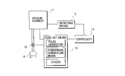
Fig. lA is a block diagram of an apparatus
designed to carry out an activation process on a
surface conduction electron-emitting device or an
electron source comprising a plurality of surface
conduction electron-emitting devices. Referring to
Fig. lA, there is shown a vacuum chamber 11 in which
a surface conduction electron-emitting device or an
electron source to be subjected to an activation
process is placed. A vacuum pump 15 and other pieces
of equipment necessary for the process are connected
to the vacuum chamber.
Reference numeral 12 denotes test equipment
for testing the electric performance of the electron-
~ - 32 - 21~3~S l
emitting device or the electron source. The equipment
comprises a number of components such as an ammeter,
a high voltage power source and various analyzers.
The electric performance may be tested in terms of the
relationships between If and Vf and between Ie and Vf,
the value of If or Ie corresponding to a particular
value of Vf, the ratio of Ie/If and their time
differentials on the electron-emitting device or the
electron source, whichever appropriate. The averages
for all the electron-emitting devices of the electron
source may also be determined if necessary.
Reference numeral 13 denotes condition set-up
means for, among others, setting up the voltage to be
applied to the device. Said means comprises a pulse
generator for generating a pulse voltage, switching
means for selecting a device to which the voltage is
applied, control means for synchronizing the operation
of the pulse generator and that of the switching means,
activation pulse voltage application means constituted
by a current amplifier and other necessary members,
atmosphere sensing means such as a pressure gauge or
a Q-mass spectrometer, means for introducing gas into
the vacuum chamber including a mass flow controller
and a solenoid valve and driver means for setting up
a desired atmosphere by regulating the mass flow
controller and the solenoid valve as well as other
necessary means.
_ _ 33 _ 2153S~4
Fig. lB is a block diagram of an apparatus
designed to carry out an activation process on an image
forming apparatus comprising a vacuum container, an
electron source and an image forming member such as a
fluorescent body. An image forming apparatus 17 is
connected to a vacuum chamber 11 by way of an exhaust
pipe 18. The atmosphere in the apparatus is controlled
by sensing the atmosphere in the vacuum chamber and
regulating the means for introducing gas a member of
the condition set-up means 13 and the gate valve 16
for evacuation.
Reference numeral 14 denote control means.
If determines the conditions for the activation process
and the timing for the process to be terminated on the
basis of a given program and the data obtained by the
test equipment 12 and drives the condition set-up means
13 to operate.
How the activation process is controlled will
be described below by referring to the flow chart of
Fig. 2.
A starting sequence is a series of operations
designed to set up initial conditions required to start
an activation process. For example, the inside of the
vacuum chamber is evacuated to a pressure lower than a
predetermined level and thereafter substances that are
necessary for the activation process such as methane,
acetone and/or other organic substances are introduced
~ 34 ~ 2153SS~
into the activation process in this step. If
necessary, the electron source folder of the apparatus
will be heated before the sequence is completed.
Thereafter, the process proceeds to a regular
sequence. This is a series of operations, during which
the atmosphere and the pulse voltage may be maintained
to respective constant levels, while the pulse wave
height and the pulse width may be varied as a function
of time according to a given program, or the atmosphere
may also be varied by gradually modifying the partial
pressures of the organic substances or by
intermittently introducing an etching gas such as
hydrogen gas for etching carbon with a predetermined
cycle.
In a sensing step, the electric performance of
the electron-emitting device is tested in a number of
aspects to better control the process. This step may
be conducted by periodically interrupting the regular
sequence and inserting a pulse voltage specifically
designed for measurement or by constantly using the
pulse voltage of the regular sequence also for this
step.
If a rectangular pulse is used for the regular
sequence of the activation process, a triangular pulse
voltage may be intermittently and additionally applied
to the ob;ect of measurement and If and/or Ie of the
object may be monitored to see its performance. The
- 35 -
21~35~4
form of the pulse voltage is not limited to triangle
and a rectangular pulse voltage having a wave height
different from that of the pulse voltage of the regular
sequence may alternatively be used.
On the other hand, if a triangular, trapezoidal
or step-like pulse is used for the regular sequence of
the activation process, the sensing step can be carried
out concurrently.
When a plurality of electron-emitting devices
are simultaneously treated for activation or an
electron source comprising a plurality of electron-
emitting devices arranged in a number of lines is
subjected to an activation process on a line by line
basis, the sensing step may be carried out on each
device or on each line of devices. Alternatively, it
may be carried out by selecting more than one devices
or lines of devices as specimens for observation.
In a deciding step, the data obtained in the
sensing sequence are checked against given data to
decide how to control the condition set-up means.
More specifically, it is decided here (1) to continue
the regular sequence, (2) to move to a processing
sequence or (3) to move to a closing sequence.
A processing sequence is a sequence of
operations for modifying the regular sequence. As a
result of this sequence, some or all of the conditions
for conducting the regular sequence may be modified or
- 36 - 21~ 3~ 4
the regular sequence may be resumed after predetermined
operational steps.
A closing se~uence is a series of operations
for terminating an activation process. In this
sequence, for example, the application of the pulse
voltage and the supply of the organic substances and
the etching gas are stopped and the inside of the
vacuum container is further evacuated to ensure that
the inner pressure falls under a given level.
5) An electron-emitting device that has been
treated in an energization forming process and an
activation process is then preferably subjected to a
stabilization process. This is a process for removing
any organic substAnc~-~ rem~Ai ni ~g in the vacuum chamber.
The vacuuming and exhausting equipment to be used for
this process preferably does not involve the use of oil
so that it may not produce any evaporated oil that can
adversely affect the performance of the treated device
during the process. Thus, the use of a sorption pump
or an ion pump may be a preferable choice.
If an oil diffusion pump or a rotary pump is
used for the activation process and the organic gas
produced by the oil is also utilized, the partial
pressure of the organic gas has to be minimized by any
means. The partial pressure of the organic gas in the
vacuum chamber is preferably lower than 1 X 10⁻⁶ Pa and
more preferably lower than 1 X 10⁻⁸ Pa if no carbon or
~- - 37 ~ 21S35~4
carbon compound is additionally deposited. The vacuum
chamber is preferably evacuated after heating the
entire chamber so that organic molecules adsorbed by
the inner walls of the vacuum chamber and the electron-
emitting device(s) in the chamber may also be easilyeliminated. While the vacuum chamber is preferably
heated to 80 to 250C for more than 5 hours in most
cases, other heating conditions may alternatively be
selected depending on the size and the profile of the
vacuum chamber and the configuration of the electron-
emitting device(s) in the chamber as well as other
considerations. The pressure in the vacuum chamber
needs to be made as low as possible and it is
preferably lower than 1 to 4 X 10⁻⁵ Pa and more
preferably lower than 1 X 10⁻⁶ Pa.
After the stabilization process, the atmosphere
for driving the electron-emitting device or the
electron source is preferably same as the one when the
stabilization process is completed, although a lower
pressure may alternatively be used without damaging the
stability of operation of the electron-emitting device
or the electron source if the organic substances in the
chamber are sufficiently removed.
By using such an atmosphere, the formation of
any additional deposit of carbon or a carbon compound
can be effectively suppressed to consequently stabilize
the device current If and the emission current Ie.
- 38 - 2153554
The performance of a electron-emitting device
prepared by way of the above processes, to which the
present invention is applicable, will be described by
referring to Figs. 8 and 9.
Fig. 8 is a schematic block diagram of an
arrangement comprising a vacuum chamber that can be
used for the above processes. It can also be used as
a gauging system for deter~i n; ng the performance of
an electron emitting device of the type under
consideration. Referring to Fig. 8, the gauging system
includes a vacuum chamber 31 and a vacuum pump 32.
An electron-emitting device is placed in the vacuum
chamber 31. The device comprises a substrate 1, a pair
of device electrodes 2 and 3, a thin film 4 and an
electron-emitting region 5. Otherwise, the gauging
system has a power source 33 for applying a device
voltage Vf to the device, an ammeter 34 for metering
the device current If running through the thin film 4
between the device electrodes 2 and 3, an anode 35 for
capturing the emission current Ie produced by electrons
emitted from the electron-emitting region of the
device, a high voltage source 36 for applying a voltage
to the anode 35 of the gauging system and another
ammeter 37 for metering the emission current Ie
produced by electrons emitted from the electron-
emitting region 5 of the device.
For determining the performance of the
- 39 - 2153S~4
electron-emitting device, a voltage between 1 and 10 KV
may be applied to the anode, which is spaced apart from
the electron-emitting device by distance H which is
between 2 and 8 mm.
Instruments including a vacuum gauge and other
pieces of equipment necessary for the gauging system
are arranged in the vacuum chamber 31 so that the
performance of the electron-emitting device or the
electron source in the chamber may be properly tested.
The vacuum pump 32 may be provided with an ordinary
high vacuum system comprising a turbo pump or a rotary
pump or an oil-free high vacuum system comprising an
oil-free pump such as a magnetic levitation turbo pump
or a dry pump and an ultra-high vacuum system
comprising an ion pump. The vacuum chamber containing
an electron source therein can be heated to 250C by
means of a heater (not shown).
Fig. 9 shows a graph schematically illustrating
the relationship between the device voltage Vf and the
emission current Ie and the device current If typically
observed by the gauging system of Fig. 8. Note that
different units are arbitrarily selected for Ie and If
in Fig. 9 in view of the fact that Ie has a magnitude
by far smaller than that of If. Note that both the
vertical and transversal axes of the graph represent a
linear scale.
As seen in Fig. 9, an electron-emitting device
- - 40 - 21535~4
according to the invention has three remarkable
features in terms of emission current Ie, which will be
described below.
(i) Firstly, an electron-emitting device
according to the invention shows a sudden and sharp
increase in the emission current Ie when the voltage
applied thereto exceeds a certain level (which is
referred to as a threshold voltage hereinafter and
indicated by Vth in Fig. 9), whereas the emission
current Ie is practically undetectable when the applied
voltage is found lower than the threshold value Vth.
Differently stated, an electron-emitting device
according to the invention is a non-linear device
having a clear threshold voltage Vth to the emission
current Ie.
(ii) Secondly, since the emission current Ie
is highly dependent on the device voltage Vf, the
former can be effectively controlled by way of the
latter.
(iii) Thirdly, the emitted electric charge
captured by the anode 35 is a function of the duration
of time of application of the device voltage Vf. In
other words, the amount of electric charge captured by
the anode 35 can be effectively controlled by way of
the time during which the device voltage Vf is applied.
Because of the above remarkable features, it
will be understood that the electron-emitting behavior
- 41 - 2153S~34
of an electron source comprising a plurality of
electron-emitting devices according to the invention
and hence that of an image-forming apparatus
incorporating such an electron source can easily be
controlled in response to the input signal. Thus, such
an electron source and an image-forming apparatus may
find a variety of applications.
On the other hand, the device current If either
monotonically increases relative to the device voltage
Vf (as shown by a solid line in Fig. 9, a
characteristic referred to as "MI characteristic"
hereinafter) or changes to show a curve (not shown)
specific to a voltage-controlled-negative-resistance
characteristic (a characteristic referred to as "VCNR
characteristic" hereinafter). These characteristics of
the device current are dependent on a number of factors
including the manufacturing method, the conditions
where it is gauged and the environment for operating
the device.
While a threshold voltage exists for If as in
the case of Ie, If lingers for a long low Vf range as
schematically shown by a broken line in Fig. 9 if the
leak current is not negligible so that the threshold
voltage will inevitably be very low.
Now, some examples of the usage of electron-
emitting devices, to which the present invention is
applicable, will be described. An electron source and
- 42 - 21S353 4
hence an image-forming apparatus can be realized by
arranging a plurality of electron-emitting devices
according to the invention on a substrate.
Electron-emitting devices may be arranged on a
substrate in a number of different modes.
For instance, a number of electron-emitting
devices may be arranged in parallel rows along a
direction (hereinafter referred to row-direction), each
device being connected by wirings at opposite ends
thereof, and driven to operate by control electrodes
(hereinafter referred to as grids) arranged in a space
above the electron-emitting devices along a direction
perpendicular to the row direction (hereinafter
referred to as column-direction) to realize a ladder-
like arrangement. Alternatively, a plurality ofelectron-emitting devices may be arranged in rows along
an X-direction and columns along an Y-direction to form
a matrix, the X- and Y-directions being perpendicular
to each other, and the electron-emitting devices on a
same row are connected to a common X-directional wiring
by way of one of the electrodes of each device while
the electron-emitting devices on a same column are
connected to a common Y-directional wiring by way of
the other electrode of each device. The latter
arrangement is referred to as a simple matrix
arrangement. Now, the simple matrix arrangement will
be described in detail.
_ ~ 43 ~ 2 1 5 3 ~ 5 1
In view of the above described three basic
characteristic features (i) through (iii) of a surface
conduction electron-emitting device, to which the
invention is applicable, it can be controlled for
electron emission by controlling the wave height and
the wave width of the pulse voltage applied to the
opposite electrodes of the device above the threshold
voltage level. On the other hand, the device does
not practically emit any electron below the threshold
voltage level. Therefore, regardless of the number
of electron-emitting devices arranged in an apparatus,
desired surface conduction electron-emitting devices
can be selected and controlled for electron emission
in response to an input signal by applying a pulse
voltage to each of the selected devices.
Fig. 8 is a schematic plan view of the
substrate of an electron source realized by arranging
a plurality of electron-emitting devices, to which the
present invention is applicable, in order to exploit
the above characteristic features. In Fig. 8, the
electron source comprises a substrate 71, X-directional
wirings 72, Y-directional wirings 73, surface
conduction electron-emitting devices 74 and connecting
wires 75. The surface conduction electron-emitting
devices may be either of the flat type or of the step
type described earlier.
There are provided a total of m X-directional
215355~
wirings 72, which are donated by Dxl, Dx2, ..., Dxm and
made of an electroconductive metal produced by vacuum
deposition, printing or sputtering. These wirings are
so designed in terms of material, thickness and width
that, if necessary, a substantially equal voltage may
be applied to the surface conduction electron-emitting
devices. A total of n Y-directional wirings are
arranged and donated by Dyl, Dy2, ..., Dyn, which are
similar to the X-directional wirings in terms of
material, thickness and width. An interlayer
insulation layer (not shown) is disposed between the m
X-directional wirings and the n Y-directional wirings
to a electrically isolate them from each other. (Both
m and n are integers).
The interlayer insulation layer (not shown) is
typically made of SiO2 and formed on the entire surface
or part of the surface of the insulating substrate 71
to show a desired contour by means of vacuum
deposition, printing or sputtering. The thickness,
material and manufacturing method of the interlayer
insulation layer are so selected as to make it
withstand the potential difference between any of the
X-directional wirings 72 and any of the Y-directional
wiring 73 observable at the crossing thereof. Each of
the X-directional wirings 72 and the Y-directional
wirings 73 is drawn out to form an external terminal.
The oppositely arranged electrodes (not shown)
- 45 -
21~35~ l
of each of the surface conduction electron-emitting
devices 74 are connected to related one of the m
X-directional wirings 72 and related one of the n
Y-directional wirings 73 by respective connecting wires
75 which are made of an electroconductive metal.
The electroconductive metal material of the
device electrodes and that of the connecting wires 75
extending from the m X-directional wirings 72 and the n
Y-directional wirings 73 may be same or contain a
common element as an ingredient. Alternatively, they
may be different from each other. These materials may
be a~lu~iately selected typically from the candidate
materials listed above for the device electrodes. If
the device electrodes and the connecting wires are made
of a same material, they may be collectively called
device electrodes without discriminating the connecting
wires.
The X-directional wirings 72 are electrically
connected to a scan signal application means (not
shown) for applying a scan signal to a selected row of
surface conduction electron-emitting devices 74. On
the other hand, the Y-directional wirings 73 are
electrically connected to a modulation signal
generation means (not shown) for applying a modulation
signal to a selected column of surface conduction
electron-emitting devices 74 and modulating the
selected column according to an input signal. Note
~ - 46 - 2153~S 4
that the drive signal to be applied to each surface
conduction electron-emitting device is expressed as the
voltage difference of the scan signal and the
modulation signal applied to the device.
With the above arrangement, each of the devices
can be selected and driven to operate independently by
means of a simple matrix wiring arrangement.
Now, an image-forming apparatus comprising an
electron source having a simple matrix arrangement as
described above will be described by referring to Figs.
11, 12A, 12B and 13. Fig. 11 is a partially cut away
schematic perspective view of the image forming
apparatus and Figs. 12A and 12B are schematic views,
illustrating two possible configurations of a
fluorescent film that can be used for the image forming
apparatus of Fig. 11, whereas Fig. 13 is a block
diagram of a drive circuit for the image forming
apparatus of Fig. 11 that operates for NTSC television
signals.
Referring firstly to Fig. 11 illustrating the
basic configuration of the display panel of the image-
forming apparatus, it comprises an electron source
substrate 71 of the above described type carrying
thereon a plurality of electron-emitting devices, a
rear plate 81 rigidly holding the electron source
substrate 71, a face plate 86 prepared by laying a
fluorescent film 84 and a metal back 85 on the inner
~ 47 ~ 215355~
surface of a glass substrate 83 and a support frame 82,
to which the rear plate 81 and the face plate 86 are
bonded by means of frit glass. Reference numeral 87
denote an envelope, which is baked to 400 to 500C
for more than 10 minutes in the atmosphere or in
nitrogen and hermetically and airtightly sealed.
In Fig. 11, reference numeral 74 denotes the
electron-emitting region of each electron-emitting
device as shown in Fig. 3 and reference numerals 72 and
73 respectively denotes the X-directional wiring and
the Y-directional wiring connected to the respective
device electrodes of each electron-emitting device.
While the envelope 87 is formed of the face
plate 86, the support frame 82 and the rear plate 81 in
the above described embodiment, the rear plate 81 may
be omitted if the substrate 71 is strong enough by
itself because the rear plate 81 is provided mainly for
reinforcing the substrate 71. If such is the case, an
independent rear plate 81 may not be required and the
substrate 71 may be directly bonded to the support
frame 82 so that the envelope 87 is constituted of a
face plate 86, a support frame 82 and a substrate 71.
The overall strength of the envelope 87 may be
increased by arranging a number of support members
called spacers (not shown) between the face plate 86
and the rear plate 81.
Figs. 12A and 12B schematically illustrate two
- 48 - 2 1 5 3 S 3 1
possible arrangements of fluorescent film. While the
fluorescent film 84 comprises only a single fluorescent
body if the display panel is used for showing black and
white pictures, it needs to comprise for displaying
color pictures black conductive members 91 and
fluorescent bodies 92, of which the former are referred
to as black stripes or members of a black matrix
depending on the arrangement of the fluorescent bodies.
Black stripes or members of a black matrix are arranged
for a color display panel so that the fluorescent
bodies 92 of three different primary colors are made
less discriminable and the adverse effect of reducing
the contrast of displayed images of external light is
weakened by blackening the surrol-n~ing areas. While
graphite is normally used as a principal ingredient of
the black stripes, other conductive material having low
light transmissivity and reflectivity may alternatively
be used.
A precipitation or printing technique is
suitably be used for applying a fluorescent material on
the glass substrate regardless of black and white or
color display. An ordinary metal back 85 is arranged
on the inner surface of the fluorescent film 84. The
metal back 85 is provided in order to enhance the
luminance of the display panel by causing the rays of
light emitted from the fluorescent bodies and directed
to the inside of the envelope to turn back toward the
_ ~ 49 ~ ~1535~4
face plate 86, to use it as an electrode for applying
an accelerating voltage to electron beams and to
protect the fluorescent bodies against damages that
may be caused when negative ions generated inside
the envelope collide with them. It is prepared by
smoothing the inner surface of the fluorescent film 75
(in an operation normally called "filming") and forming
an Al film thereon by vacuum deposition after forming
the fluorescent film 84.
A transparent electrode (not shown) may be
formed on the face plate 86 facing the outer surface of
the fluorescent film 84 in order to raise the
conductivity of the fluorescent film 84.
Care should be taken to accurately align each
set of color fluorescent bodies and an electron-
emitting device, if a color display is involved, before
the above listed components of the envelope are bonded
together.
A forming process is carried out for the
surface conduction electron-emitting devices in a
manner as will be described hereinafter.
Then an activation process is carried out as
follows. Fig. lB illustrates an arrangement that can
suitably be used for this process.
The image forming apparatus that has been
hermetically and airtightly sealed as described above
is connected to a vacuum chamber by way of an exhaust
- 50 - 21~33~ 4
pipe. The vacuum chamber is evacuated by means of a
vacuum pump until the inner pressure of the chamber
gets to a predetermined level.
The arrangement comprises test equipment,
condition setup means and control means similar to
those of the arrangement for activating a surface
conduction electron-emitting device or an electron
source comprising a plurality of such devices that is
described earlier. However, since it is difficult to
directly monitor the atmosphere in the inside of the
envelope of the image forming apparatus during the
activation process, the atmosphere in the inside of the
vacuum chamber is normally monitored and controlled to
control that of the apparatus.
For controlling the atmosphere in the inside of
the vacuum chamber, the procedure as illustrated in the
flow chart of Fig. 2 is used as in the case of
activating a surface conduction electron-emitting
device or an electron source comprising a plurality of
such devices.
The envelope 87 is evacuated by means of an
appropriate vacuum pump such as an ion pump or a
sorption pump that does not involve the use of oil,
while it is being heated as in the case of the
stabilization process, until the atmosphere in the
inside is reduced to a degree of vacuum of 10-5 Pa
cont~;n;ng organic substances to a sufficiently low
- 51 - 21535~4
level and then it is hermetically and airtightly
sealed. A getter process may be conducted in order to
maintain the achieved degree of vacuum in the inside of
the envelope 87 after it is sealed. In a getter
process, a getter arranged at a predetermined position
in the envelope 87 is heated by means of a resistance
heater or a high frequency heater to form a film by
vapor deposition immediately before or after the
envelope 87 is sealed. A getter typically contains Ba
as a principal ingredient and can maintain a degree of
vacuum between 1 X lo-4 and 1 X 10⁻⁵ by the adsorption
effect of the vapor deposition film.
Now, a drive circuit for driving a display
panel comprising an electron source with a simple
matrix arrangement for displaying television images
according to NTSC television signals will be described
by referring to Fig. 13. In Fig. 13, reference numeral
101 denotes a display panel. Otherwise, the circuit
comprises a scan circuit 102, a control circuit 103, a
shift register 104, a line memory 105, a synchronizing
signal separation circuit 106 and a modulation signal
generator 107. Vx and Va in Fig. 13 denote DC voltage
sources.
The display panel 101 is connected to external
circuits via terminals Doxl through Doxm, Doyl through
Doyn and high voltage terminal Hv, of which terminals
Doxl through Doxm are designed to receive scan signals
- 52 - 21535~
for sequentially driving on a one-by-one basis the rows
(of N devices) of an electron source in the apparatus
comprising a number of surface-conduction type
electron-emitting devices arranged in the form of a
matrix having M rows and N columns.
On the other hand, terminals Doyl through Doyn
are designed to receive a modulation signal for
controlling the output electron beam of each of the
surface-conduction type electron-emitting devices of
a row selected by a scan signal. High voltage terminal
Hv is fed by the DC voltage source Va with a DC voltage
of a level typically around 10 KV, which is
sufficiently high to energize the fluorescent bodies
of the selected surface-conduction type electron-
emitting devices.
The scan circuit 102 operates in a manner asfollows. The circuit comprises M switching devices (of
which only devices Sl and Sm are specifically indicated
in Fig. 13), each of which takes either the output
voltage of the DC voltage source Vx or O[V] (the ground
potential level) and comes to be connected with one of
the terminals Doxl through Doxm of the display panel
101. Each of the switching devices S1 through Sm
operates in accordance with control signal Tscan fed
from the control circuit 103 and can be prépared by
combining transistors such as FETs.
The DC voltage source Vx of this circuit is
_ - 53 - 2153S5~
designed to output a constant voltage such that any
drive voltage applied to devices that are not being
scanned due to the performance of the surface
conduction electron-emitting devices (or the threshold
voltage for electron emission) is reduced to less than
threshold voltage.
The control circuit 103 coordinates the
operations of related components so that images may be
appropriately displayed in accordance with externally
fed video signals. It generates control signals Tscan,
Tsft and Tmry in response to synchronizing signal Tsync
fed from the synchronizing signal separation circuit
106, which will be described below.
The synchronizing signal separation circuit 106
separates the synchronizing signal component and the
lumin~nce signal component form an externally fed NTSC
television signal and can be easily realized using a
popularly known frequency separation (filter) circuit.
Although a synchronizing signal extracted from a
television signal by the synchronizing signal
separation circuit 106 is constituted, as well known,
of a vertical synchronizing signal and a horizontal
synchronizing signal, it is simply designated as Tsync
signal here for convenience sake, disregarding its
component signals. On the other hand, a lum;n~nce
signal drawn from a television signal, which is fed to
the shift register 104, is designed as DATA signal.
- - 54 - 21~ 3~ ~
The shift register 104 carries out for each
line a serial/parallel conversion on DATA signals that
are serially fed on a time series basis in accordance
with control signal Tsft fed from the control circuit
103. (In other words, a control signal Tsft operates
as a shift clock for the shift register 104.) A set of
data for a line that have undergone a serial/parallel
conversion (and correspond to a set of drive data for N
electron-emitting devices) are sent out of the shift
register 104 as n parallel signals Idl through Idn.
The line memory 105 is a memory for storing a
set of data for a line, which are signals Idl through
Idn, for a required period of time according to control
signal Tmry coming from the control circuit 103. The
stored data are sent out as I'dl through I'dn and fed
to modulation signal generator 107.
Said modulation signal generator 107 is in fact
a signal source that appropriately drives and modulates
the operation of each of the surface-conduction type
electron-emitting devices and output signals of this
device are fed to the surface-conduction type electron-
emitting devices in the display panel 101 via terminals
Doyl through Doyn.
As described above, an electron-emitting
device, to which the present invention is applicable,
is characterized by the following features in terms of
emission current Ie. Firstly, there exists a clear
_ 55 - 21S3~54
threshold voltage Vth and the device emit electrons
only a voltage exceeding Vth is applied thereto.
Secondly, the level of emission current Ie changes as a
function of the change in the applied voltage above the
threshold level Vth, although the value of Vth and the
relationship between the applied voltage and the
emission current may vary depending on the materials,
the configuration and the manufacturing method of the
electron-emitting device. More specifically, when a
pulse-shaped voltage is applied to an electron-emitting
device according to the invention, particularly no
emission current is generated so far as the applied
voltage remains under the threshold level, whereas an
electron beam is emitted once the applied voltage rises
above the threshold level. It should be noted here
that the intensity of an output electron beam can be
controlled by changing the peak level Vm of the pulse-
shape~ voltage. Additionally, the total amount of
electric charge of an electron beam can be controlled
by varying the pulse width Pw.
Thus, either modulation method or pulse width
modulation may be used for modulating an electron-
emitting device in response to an input signal. With
voltage modulation, a voltage modulation type circuit
is used for the modulation signal generator 107 so that
the peak level of the pulse shaped voltage is modulated
according to input data, while the pulse width is held
2153~4
~ - 56 -
constant.
With pulse width modulation, on the other hand,
a pulse width modulation type circuit is used for the
modulation signal generator 107 so that the pulse width
of the applied voltage may be modulated according to
input data, while the peak level of the applied voltage
is held constant.
Although it is not particularly mentioned
above, the shift register 104 and the line memory 105
may be either of digital or of analog signal type so
long as serial/parallel conversions and storage of
video signals are conducted at a given rate.
If digital signal type devices are used, output
signal DATA of the synchronizing signal separation
circuit 106 needs to be digitized. However, such
conversion can be easily carried out by arranging an
A/D converter at the output of the synchronizing signal
separation circuit 106. It may be needless to say that
different circuits may be used for the modulation
signal generator 107 depending on if output signals of
the line memory 105 are digital signals or analog
signals. If digital signals are used, a D/A converter
circuit of a known type may be used for the modulation
signal generator 107 and an amplifier circuit may
additionally be used, if necessary. As for pulse width
modulation, the modulation signal generator 107 can be
realized by using a circuit that combines a high speed
21~3S~
- - 57 -
oscillator, a counter for counting the number of waves
generated by said oscillator and a comparator for
comparing the output of the counter and that of the
memory. If necessary, an amplifier may be added to
amplify the voltage of the output signal of the
comparator having a modulated pulse width to the level
of the drive voltage of a surface-conduction type
electron-emitting device according to the invention.
If, on the other hand, analog signals are used
with voltage modulation, an amplifier circuit
comprising a known operational amplifier may suitably
be used for the modulation signal generator 107 and a
level shift circuit may be added thereto if necessary.
As for pulse width modulation, a known voltage control
type oscillation circuit (VC0) may be used with, if
necessary, an additional amplifier to be used for
voltage amplification up to the drive voltage of
surface-conduction type electron-emitting device.
With an image forming apparatus having a
configuration as described above, to which the present
invention is applicable, the electron-emitting devices
emit electrons as a voltage is applied thereto by way
of the external terminals Doxl through Doxm and Doyl
through Doyn. Then, the generated electron beams are
accelerated by applying a high voltage to the metal
back 85 or a transparent electrode (not shown) by way
of the high voltage terminal Hv. The accelerated
2153~S l
- 58 -
electrons eventually collide with the fluorescent film
84, which by turn glows to produce images.
The above described configuration of image
forming apparatus is only an example to which the
present invention is applicable and may be subjected to
various modifications. The TV signal system to be used
with such an apparatus is not limited to a particular
one and any system such as NTSC, PAL or SECAM may
feasibly be used with it. It is particularly suited
for TV signals involving a larger number of scanning
lines (typically of a high definition TV system such as
the MUSE system) because it can be used for a large
display panel comprising a large number of pixels.
Now, an electron source comprising a plurality
of surface conduction electron-emitting devices
arranged in a ladder-like manner on a substrate and an
image-forming apparatus comprising such an electron
source will be described by referring to Figs. 14 and
15.
Firstly referring to Fig. 14, reference numeral
110 denotes an electron source substrate and reference
numeral 111 denotes a surface conduction electron-
emitting device arranged on the substrate, whereas
reference numeral 112 denotes common wirings Dxl
through DxlO for connecting the surface conduction
electron-emitting devices. The electron-emitting
devices 111 are arranged in rows (to be referred to as
- 59 _ 21~3554
device rows hereinafter) to form an electron source
comprising a plurality of device rows, each row having
a plurality of devices. The surface conduction
electron-emitting devices of each device row are
electrically connected in parallel with each other by a
pair of common wirings so that they can be driven
independently by applying an appropriate drive voltage
to the pair of common wirings. More specifically, a
voltage exceeding the electron emission threshold level
is applied to the device rows to be driven to emit
electrons, whereas a voltage below the electron
emission threshold level is applied to the rem~ining
device rows. Alternatively, any two external terminals
arranged between two adjacent device rows can share a
single common wiring. Thus, of the common wirings Dx2
through Dx9, Dx2 and Dx3 can share a single common
wiring instead of two wirings.
Fig. 15 is a schematic perspective view of the
display panel of an image-forming apparatus
incorporating an electron source having a ladder-like
arrangement of electron-emitting devices. In Fig. 15,
the display panel comprises grid electrodes 120, each
provided with a number of bores for allowing electrons
to pass therethrough and a set of external terminals
Doxl, Dox2, ..., Doxm along with another set of
external terminals G1, G2, ..., Gn connected to the
respective grid electrodes 120 and an electron source
- 60 - 2153S~4
substrate 71. The image forming apparatus differs from
the image forming apparatus with a simple matrix
arrangement of Fig. 11 mainly in that the apparatus of
Fig. 15 has grid electrodes 120 arranged between the
electron source substrate 71 and the face plate 86.
In Fig. 15, the stripe-shaped grid electrodes
120 are arranged between the substrate 71 and the face
plate 86 perpendicularly relative to the ladder-like
device rows for modulating electron beams emitted from
the surface conduction electron-emitting devices, each
provided with through bores 121 in correspondence to
respective electron-emitting devices for allowing
electron beams to pass therethrough. Note that,
however, while stripe-shaped grid electrodes are shown
in Fig. 15, the profile and the locations of the
electrodes are not limited thereto. For example, they
may alternatively be provided with mesh-like openings
and arranged around or close to the surface conduction
electron-emitting devices.
The external terminals Dl through Dm and the
external terminals for the grids Gl through Gn are
electrically connected to a control circuit (not
shown).
An image-forming apparatus having a
configuration as described above can be operated for
electron beam irradiation by simultaneously applying
modulation signals to the rows of grid electrodes for a
`~ - 61 - 21~3~4
single line of an image in synchronism with the
operation of driving (scanning) the electron-emitting
devices on a row by row basis so that the image can be
displayed on a line by line basis.
Thus, a display apparatus according to the
invention and having a configuration as described above
can have a wide variety of industrial and commercial
applications because it can operate as a display
apparatus for television broadcasting, as a terminal
apparatus for video teleconferPnc;ng, as an editing
apparatus for still and movie pictures, as a terminal
apparatus for a computer system, as an optical printer
comprising a photosensitive drum and in many other
ways.
Now, the present invention will be described by
way of examples.
[Example 1]
Figs. 3A and 3B schematically illustrate an
electron-emitting device prepared in this example.
While onIy a single device is shown for the purpose of
simplification, five devices are arranged in parallel
on a substrate of an electron source prepared in this
example. The process employed for manufacturing the
electron source will be described by referring to Figs.
5A through 5C.
Step-a:
After thoroughly cleansing a soda lime glass
- 62 - 2153~54
plate, a silicon oxide film was formed thereon to a
thickness of 0.5 ,um by sputtering to produce a
substrate 1, on which a pattern of photoresist (RD-
2000N-41: available from Hitachi Chemical Co., Ltd.)
corresponding to the pattern of a pair of electrodes
having openings was formed. Then, a Ti film and an Ni
film were sequentially formed to respective thicknesses
of 5 nm and 100 nm by vacuum deposition. Thereafter,
the photoresist was dissolved by an organic solvent and
the Ni/Ti film was lifted off to produce a pair of
device electrodes 2 and 3. The device electrodes was
separated by distance L of 3 ~m and had a width W of
300 ~m. (Fig. 5A)
Step-b:
A Cr film was formed on the device to a
thickness of 100 nm by vacuum deposition and then
an opening corresponding the pattern of an
electroconductive thin film was formed by
photolithography. Thereafter, a Cr mask was
formed for forming an electroconductive thin film.
Thereafter, a solution of Pd-amine complex
(ccp4230: available from Okuno Pharmaceutical Co.,
Ltd.) was applied to the Cr film by means of a spinner
and baked at 300C for 10 minutes to produce a fine
particle film containing PdO as a principal ingredient.
The film had a film thickness of 10 nm.
Step-c:
- 63 - 2153~4
The Cr mask was removed by wet-etching and the
PdO fine particle film was lifted off to obtain an
electroconductive thin film 4 having a desired profile.
The electroconductive thin film showed an electric
resistance of Rs = 2 x 10⁴ Q/~ and had a thickness of
10 nm. (Fig. 5B)
Step-d:
The electron source 43 was placed on a sample
holder 42 in the vacuum chamber 41 of a gauging system
as illustrated in Fig. 16A and the vacuum chamber 41
was evacuated by means of a vacuum pump unit 44 to a
pressure of 1.3 x 10⁻³ Pa. The vacuum pump unit 44
was a high vacuum pump unit comprising a turbo pump
and a rotary pump. The vacuum pump unit 44
additionally comprises an ion pump for producing
an ultra-high vacuum condition and these pumps could
be selectively used. The unit further comprises a
driver 45 for switching the pumps, opening the valve
of a vacuum gauge and turning on and off the pumps.
Subsequently, a pulse voltage was applied to each of
the devices by way of a drive circuit 46 to carry out
an electric forming process and produce an electron
emitting region. The pulse voltage was a triangular
pulse voltage whose peak value gradually increased with
time as shown in Fig. 6B. The pulse width of Tl = 1
msec and the pulse interval of T2 = 10 msec were used.
During the electric forming process, an extra pulse
~ - 64 - 2153S54
voltage of 0.1 V was inserted into intervals of the
forming pulse voltage in order to determine the
resistance of the electron emitting region and the
electric forming process was terminated when the
resistance exceeded 1 MQ.
The peak value of the pulse voltage was 5.0
to 5.1 V when the forming process was terminated.
Step-e:
Subsequently, the electron source was subjected
to an activation process, maint~; ni ng the inside
pressure of the vacuum chamber to about 1.3 x 10⁻³ Pa.
A rectangular pulse voltage with a height of
14 V was applied to each of the devices by way of
the drive circuit 46. While the system of Fig. 6B
comprised an ammeter 47, it was not used in this
process. The system further comprised an anode 48 for
capturing electrons emitted from the electron source
43, to which a voltage that was higher than the voltage
applied to the electron source 43 by +1 KV was applied
from a high voltage source 49. The devices and the
anode were separated by a distance of H = 4 mm. The
emission current Ie of each device was detected by
another ammeter 50.
The Ie detected by the ammeter 50 is fed to a
control unit 55.
In this example, the control unit 55 was so
designed that, once the emission current Ie of each
_ - 65 - 21~355~
device reached 0.9 ~uA, it caused the drive circuit 46
to suspend the pulse voltage being applied to the
device.
Step-f:
Thereafter, a stabilization process was carried
out. In this step, the ultra-high vacuum ion pump of
the vacuum pump unit 44 was used and the electron
source was heated to 120C by means of a heater (not
shown) contained in the sample holder 42 for 10 hours.
It was detected by atmosphere sensing means 53
(comprising an ionization vacuum gauge and a Q-mass
spectrometer in this example) that the inner pressure
of the vacuum chamber 41 was about 6.3 x 10⁻⁵ Pa (the
partial pressure of the organic substances having the
origin in the oil of the high vacuum pump used in
Steps-d and e being less than 6.3 x 10⁻⁶ Pa). Reference
numeral 54 denotes a drive circuit for the atmosphere
sensing means.
A pulse voltage of 14 V (with a pulse width of
100 ~usec.) was applied to the electron source for some
time under this condition until Ie was found to have
reached a saturated state.
The electron source was tested for its
performance by applying a triangular pulse voltage
(with a pulse width of 100 ~usec) of 14 V. All the
devices performed similarly in terms of MI.
[Example 2]
_ - 66 - 21~ 3'j~ ~
Steps-a through d of Example 1 were also
followed in this example and then an activation process
was started as in the case of Step-e. Ie of device #5
rose a little slower than those of devices #1 through
#4. The control unit 55 continuously calculated the
rate of increase of Ie detected by the ammeter 50 and
determined the average over a given period of time. If
the rate at a selected moment differed beyond a given
limit on any of the devices, the pulse height of the
pulse voltage being applied to the device was modified
as a function of the difference. As a result, only the
pulse height for device #5 rose to 15 V in the course
of the activation process. A requirement of Ie 2 0.9
~A as given for terminating the process. Thus, the
application of a pulse voltage was terminated for each
device as soon as Ie got to 0.9 ~A for the device.
Subsequently, an activation process was carried
out as in the case of Step-f of Example 1 and then the
performance of each devices was tested.
All the devices performed similarly in terms
of MI.
[Example 3]
Steps-a through d of Example 1 were also
followed for all the devices in this example and then
an activation process was started as in the case of
Step-e. Ie of device #5 rose a little slower than
those of devices #1 through #4. The programmed
- 67 - 21533~4
standard process was so designed that a pulse voltage
with a pulse height of 14 V and a rectangular pulse
width of 30 msec. was applied for activation and, after
a certain duration of activation, the pulse width was
changed to 20 msec. before terminating the activation
process. The control unit 55 continuously calculated
the rate
of increase of Ie detected by the ammeter 50 and
determined the average over a given period of time.
If the rate at a selected moment differed beyond a
given limit on any of the devices, the pulse width
of the pulse voltage being applied to the device was
modified as a function of the difference after the
change of the pulse width. The standard process was
carried out for devices #1 through #4 and the pulse
width was changed to 20 msec. On the other hand, for a
device #5, a pulse voltage with a pulse width of 30
msec. was applied all the way until the end of the
activation process. The application of the pulse
voltage was terminated for each device as soon as Ie
got to
0.9 ~A for the device.
Subsequently, an activation process was carried
out as in the case of Step-f of Example 1 and then
the perfo. ~nce of each devices was tested. All the
devices performed similarly in terms of MI.
[Comparative Example 1]
~ - 68 _ 2153~4
Steps-a through d of Example 1 were also
followed and then an activation process was carried
out for all the devices in this example by applying a
rectangular pulse voltage of 14 V. Thereafter, Step-f
was also followed as in the case of Example 1 and a
triangular pulse voltage of 14 V was applied to test
the performance of each device. While all the device
performed similarly in terms of MI, devices #1 through
#4 showed slight deviations in the performance when
compared with Example 1 through 3 described above.
If and Ie of device #5 were respectively about 2/3
and 1/2 of those of the other devices.
The devices of Examples 1 through 3 and
Comparative Example 1 were prepared by following
Steps-a through d and device #5 revealed the tendency
of performing poorly in each case. While it may be
reasonable to assume that this fact was attributable
to something in Steps-a through d, no exact reason
could not be found. However, it was found that this
problem can be solved by carrying out an activation
process by means of an apparatus according to the
invention.
While the deviations in the performance
of devices #l through #4 were minute and might be
attributable to an accident, such deviations could
be removed by a method according to the invention.
[Example 4, Comparative Example 2]
~_ - 69 - 21535~
The devices used in these Example and
Comparative Example had a profile as shown in Fig. 3
and a total of 48 devices were arranged in a single row
on a substrate for each example as schematically shown
in Fig. 17.
Steps-a through c were followed and an
electroconductive thin film of fine PdO particles was
formed as in the case of Example 1. Thereafter, a
forming process was carried out by following Step-d
of Example 1. The inner pressure of the vacuum chamber
was 2.7 x 10⁻⁴ Pa.
Step-e:
Subsequently, an activation process was carried
out.
The vacuum chamber was so operated by the
control unit 55 that, after evacuating the vacuum
chamber by means of an ion pump to about 10-6 Pa,
acetone was introduced into the chamber by regulating
a gas supply unit 51 and a solenoid valve 52 until the
inner pressure of the vacuum chamber rose to 2.7 x 10~
Pa. At the same time, the drive circuit of the vacuum
pump unit was also operated by the control unit 55 to
regulate the evacuation rate by means of a gate valve.
The devices were numbered serially from No. 1
through No. 48 and the devices with even numbers were
processed in a manner as follows.
The pulse voltage applied to the devices had a
`~ _ 70 _ 21~3~4
rectangular pulse wave whose polarity was alternately
inverted as shown in Fig. 18B. The pulse width was
equal to Tl = 1 msec. for both polarities and the pulse
interval was equal to T2 = 10 msec. In other words,
the pulse had a period of 20 msec. and a frequency of
50 Hz.
The pulse height was initially 10 V and
increased at a rate of 0.2 V/min. until it got to 18 V.
Using this for a regular sequence and a
triangle pulse voltage having the same pulse height
was additionally applied for every 30 seconds to
detect the relationship between If and Vf.
In these examples, If was so controlled that
it would not exceed a predetermined level for Vf2 that
was lower than Vact. Specifically, the relationship
Vf2 = 0.8 X Vact was used and the regular sequence
was continued as long as a requirement of If(Vf2) <
0.05 mA was satisfied.
If, to the contrary, the above requirement
was not met, or If(Vf2) 2 0.05 mA was observed, Vact
was increased by 0.2 V and the regular sequence was
resumed.
Under this condition, the If-Vf relationship
was such that If lingers for along low Vf range as
schematically shown by a broken line in Fig. 9 to push
up the value of If(Vf2). The inventors of the present
invention assumes that this was caused by a small
~ - 71 - 2153~ a ~
route for a leak current formed by carbon or a carbon
compound in the electroconductive thin film between
the anode and the cathode that were oppositely disposed
with an electron emitting region arranged therebetween.
This lingering phenomenon on the If-Vf relationship was
dissolved by raising Vact probably because the carbon
or the carbon compound forming the route for a leak
current was evaporated by Joule's heat.
If If(Vf2) raised again after returning to the
regular sequence, the above operation was repeated to
obtain a electron-emitting device that showed a desired
performance.
When Vact reached 18 V, the operation proceeded
to a closing sequence if If 2 2 mA was observed to
terminate the activation process. If the above
requirement was not met, Vact = 10 V was resumed
and the regular sequence was repeated.
For the purpose of comparison, a rectangular
pulse voltage whose polarity alternately inverted as
in the case of the above regular sequence was applied
to the odd-numbered devices and Vact was raised from
Vact = 10 V to Vact = 18 V at a rate of 0.2 V/min. so
that the sequence was terminated in 40 minutes. These
devices are referred to as those of Comparative Example
2.
Thereafter, the vacuum chamber and the
electron-emitting devices in there were heated to 180C
215~S~ 4
_ - 72 -
for 2 hours and a stabilization process was carried out
on the devices, while evacuating the vacuum chamber by
means of an ion pump. If of a device normally differs
after the end of an activation process and after the
end of a stabilization process.
Then, a triangular pulse voltage of 16 V was
applied to the devices to see their performance. The
inner pressure of the vacuum chamber was held to 1.3 x
10-7 Pa and the anode and the electron-emitting devices
were separated from each other by 4 mm, while the
potential difference was held to 1 KV.
The value of If for V = 8 V was expressed by
Ifmid. This value corresponds to the so-called "half
selection current" when an electron source comprising a
plurality of electron-emitting devices arranged for
simple matrix wiring is drive to operate and should
preferably be as small as possible. The table below
shows the average values and the deviation of Ie for
the 24 devices of Example 4 and those of Comparative
Example 2.
If(mA) Ie(~A) ~(%) Ifmid(mA) ~Ie(~)
~x~rle 4 1.1 1.1 0.10 0.005 +7
Comparative 1.0 0.6 0.06 0.01 +12
Example 2
[Example 5, Comparative Example 3]
2153~4
- 73 -
Devices were prepared as in the case of Example
4 and a forming process was carried out on them.
Thereafter, in
Step-e:
The vacuum chamber was evacuated by means of
an ion pump and then n-h~x~ne was introduced into the
chamber by controlling the gas supply unit 51 and the
solenoid valve 52 so that the inner pressure of the
chamber was maintained to 2.7 X 10⁻³ Pa.
A trapezoidal pulse voltage of with a pulse
height of 16 V as shown in Fig. 7A was applied to the
devices. The rising edge of the pulse was inclined and
this inclination was used to determine the If-Vf and
Ie-Vf relationships. Otherwise, the pulse was defined
by T2 = 10 msec., T3 = 10 ,usec and the pulse width T1
that was gradually increased from 10 ~sec. at a rate
to become twice as large in 5 minutes for a regular
sequence. The anode and the devices were separated
from each other by 4 mm and the potential difference
was 1 KV.
From the observed performance, threshold
voltages Vtf and Vte were defined as the respective
voltage values for 1/100 of the If and Ie values for
Vact = 16 V. As in the case of Example 4, the regular
sequence was continued on the even-numbered devices as
long as the requirement of Vte - Vtf < 1 V was met,
whereas, whenever it was found that the requirement was
2153~4
_ - 74 -
not met, T2 was doub~ed at that moment and then the
regular sequence was resumed. When T1 2 1 msec. was
observed, the operation proceeds to a closing sequence
if Ie 2 2 ,uA. If otherwise, T1 = 10 ,usec. was
established and then the regular sequence was resumed.
If n-hexane was used as an organic substance,
an activation process could be carried out with a
partial pressure lower than that of acetone. If the
acetone shows a partial pressure of 10~1 as in the
case of Example 4, an electric discharge can occur to
destroy the electron-emitting devices being treated
for an activation process when a high voltage is
applied to the anode in order to observe Ie. To the
contrary, n-hex~ne having a relatively low partial
pressure was used in these examples and, therefore,
the activation process could be carried out smoothly,
while observing Ie without any danger.
For the purpose of comparison, a similar pulse
voltage was applied to the odd-numbered devices for
about 30 minutes to an activation process, during
which Tl was increased from 10 ,usec. to 1 msec.
These devices are referred to as those of Comparative
Example 3.
Thereafter, a stabilization process was carried
out as in the case of Example 4. The results are shown
in the table below. Note that both If and
Ie of a device normally differ after the end of an
21~3~54
- 75 -
activation process and after the end of a stabilization
process.
If(mA) Ie(~A) ~(~) Ifmid(mA) ~Ie(~)
Example 5 1.0 1.1 0.11 0.007 +10
Comparative 0.9 0.9 0.10 0.010 +12
Example 3
[Example 6, Comparative Example 4]
Devices were prepared as in the case of Example
4 and a forming process was carried out on them.
Thereafter, in
Step-e:
The vacuum chamber was evacuated by means of
an ion pump and then dodecane was introduced into the
chamber by controlling the vacuum pump drive circuit
45, the gas supply unit 51 and the solenoid valve 52
so that the inner pressure of the chamber was
maintained to 2.7 X 10⁻³ Pa. A step-shaped pulse
voltage with a pulse of Tl = 1 msec., a pulse interval
of T2 = 10 msec., a pulse height of 16 V and a reduced
pulse height of 12 V as shown in Fig. 7B was applied.
The width of the portion of the reduce height was equal
to T3 = 100 ~sec.
The pulse voltage was continued for a regular
sequence.
As in the case of Examples 4 and 5, the even-
21S3~54
- - 76 -
numbered devices were treated in a following manner.
While monitoring both If and Ie, the pulse
height was raised to 18 V for only 5 seconds when If(Vf
= 12 V) 2 0.05 mA was observed and then the regular
sequence was resumed.
The activation process was terminated and a
closing sequence was started when Ie(Vf = 16 V) 2 2 ,uA
was observed.
The above 16 V pulse voltage was applied for 30
minutes to the odd-numbered devices to terminate an
activation process. These devices are referred to as
those of Comparative Example 4.
Thereafter, a stabilization process was carried
out as in the case of Examples 4 and 5.
The results are shown in the table below.
If(mA) Ie(~A) ~(%) Ifmid(mA) ~Ie(%)
Example 6 1.0 1.2 0.12 0.006 +9
Comparative 1.5 0.9 0.06 0.011 +14
Example 4
[Example 7]
Devices were activated by a regular sequence
like the one of Example 6. The high voltage power
source for applying a high voltage to the anode for
monitoring Ie was turned off when If (Vf = 12 V) 2 0.05
mA was observed and then hydrogen gas was introduced
21S3~5 4
_ - 77 -
into the vacuum chamber by controlling the gas supply
unit 51 and the solenoid valve 52. The gas flow rate
was so regulated that the partial pressure of the
hydrogen gas reached about 0.13 Pa. 20 seconds
thereafter, the solenoid valve was closed to stop
the gas supply and the high voltage power source was
turned on to resume the regular sequence.
The activation process was terminated as in the
case of Example 6.
Thereafter, a stabilization process was carried
out. The results are shown in the table below.
If(mA) Ie(~A) ~(%) Ifmid(mA) ~Ie(~)
Example 7 0.8 1.2 0.13 0.005 +9
[Example 8, Comparative Example 5]
Devices were prepared as in the case of Example
4 and a forming process was carried out on them.
Thereafter, in
Step-e:
The vacuum chamber was evacuated by means of an
ion pump and then dodecane was introduced into the
chamber by controlling the vacuum pump drive circuit
45, the gas supply unit 51 and the solenoid valve 52 so
that the inner pressure of the chamber was maint~ine~
to 2.7 X 10~1 Pa for initialization.
A pulse voltage like that of example 4 was
applied, although the pulse height was constantly 16 V.
- 78 - 21535~
As in the case of Examples 4 through 6, the
even-numbered devices are subjected to an activation
process as described below.
When If > 1.5mA was obserbed, a quantity of
introducing acetone was reduced until its partial
pressure became to 1/10. This operation was repeated
until a partial pressure of aetone became lower than
2.7 X lO~sPa. Then the activation process was
terminated to start a closing sequence.
A pulse voltage same as above was applied to
the odd-numbered devices for 30 minutes in an
atmosphere having a partial pressure of acetone equal
to 2.7 X Io-2 Pa. The devices are referred to as those
of Comparative Example 5.
Thereafter, a stabilization process was carried
out as in the case of Examples 4 through 7. The
results are shown in the table below.
If(mA) Ie(,uA) ~(%) Ifmid(mA) ~Ie(%)
Example 8 1.2 1.5 0.13 0.011 +7
Comparative 1.0 0.9 0.09 0.010 ~13
Example 5
[Example 9, Comparative Example 6]
In this example 4, devices were prepared on
a substrate.
Steps-a through d of Example 1 were also
_ _ 79 _ 2153~54
followed in this example and thereafter in
Step-e:
An activation process was carried out. The
inner pressure of the vacuum chamber was 2.7 X 10⁻³ Pa.
The vacuum pump used here was a high vacuum type pump.
A rectangular pulse voltage as shown in Fig.
18A was applied to the devices. The pulse voltage had
a pulse height of 14 V, a pulse width of 100 ~sec.
and a pulse interval of 10 msec.
The activation process was carried out,
monitoring the device current If and the emission
current Ie. The electron-emitting devices were
separated from the anode by 4 mm and the anode had
a potential of 1 KV.
The control unit used for this example read
the data of the Ie detecting ammeter and calculated
the increasing ratio of Ie with time, or dIe/dt to
determine a maximum for Ie, or dIe/dt = 0. In
practice, since the observed value of Ie could contain
noise, the value was integrated with a time constant
of 1 second to find out the time when dIe/dt remained
almost equal to 0 for 1 minute and the activation
process was terminated at that time.
The activation process was in reality carried
out on two of the four devices. The process was
terminated in about 60 minutes for both of the devices.
For comparison, an activation process was also
2153~54
- 80 -
carried out for the remaining two devices for 40
minutes, using the same pulse voltage.
Thereafter, the vacuum pump was switched to an
ion pump to carry out a stabilization process under the
condition of Step-f of Example 1. While both Ie and
If decreased temporarily during the process, they
eventually converged to respective constant values.
The results are shown in the table below.
If(mA)Ie(,uA)
Example 9 1.5 1.5 0.1
Comparative 1.2 1.2 0.1
Example 6
[Example 10]
A dry pump (scroll pump) and a magnetic
floating type turbo pump were used for the vacuum pump
unit of this Example. With this arrangement, the
organic substance involved could be effectively
suppressed from diffusion into the vacuum chamber
so that a satisfactory vacuum condition can be
established for the following processes.
Steps-a through d were also followed in this
example as in the case of Example 9 and thereafter in
Step-e:
Acetone was introduced into the vacuum chamber
by controlling the gas supply unit 51 and the solenoid
- 81 - 2153~.~ 4
valve 52. The partial pressure of acetone was
regulated to 2.7 X 10⁻³ Pa. The vacuum pump used
here was a high vacuum type pump.
A rectangular pulse voltage similar to that
of Example 9 was applied. An activation process was
carried out for 50 minutes, monitoring the device
current If and the emission current Ie.
Then, the supply of acetone was suspended and
the inner pressure of the vacuum chamber was reduced
further to about 1.3 X 10⁻⁵ Pa. Thereafter, a
stabilization process was carried out as in the case
of Example 1.
If(mA) Ie(~uA)
Example 10 1.3 1.3 0.1
[Example 11]
Steps-a through d were also followed in this
example as in the case of Example 9 and thereafter in
Step-e:
The inner pressure of the vacuum chamber was
reduced to about 2.0 X 10⁻³ Pa by means of a high vacuum
pump unit comprising a turbo pump and a rotary pump.
Like Example 9, an activation process was
carried out, monitoring the device current If and the
emission current Ie. The control unit calculated ~ =
Ie/If from the monitored value of If and Ie and then
~ - 82 - 2 1 ~ 3 ~ ~ 1
further calculated d~/dt. The activation process was
terminated when a maximum value of ~ or d~/dt=0 was
obtained.
The activation process continued for about 2
minutes.
Then, the vacuum pump was switched to an ion
pump to further evacuate the vacuum chamber and a
stabilization process as performed as in the case of
Example 1.
The results are shown in Table below.
If(mA) Ie(,uA) ~(%)
Example 11 0.17 0.50 0.3
[Example 12]
In this example, the present invention was
applied to an electron source prepared by arranging
plurality of surface conduction electron-emitting
devices on a substrate and wiring them to form a
matrix. The electron source had 100 devices in both
the X- and Y-directions.
Step-A:
After thoroughly cleansing a soda lime glass
plate a silicon oxide film was formed thereon to a
thickness of 0.5 ~m by sputtering to produce a
substrate 1, on which Cr and Au were sequentially laid
to thicknesses of 5 nm and 600 nm respectively and then
- 83 _ 21~3~5~
-
a photoresist (AZ1370: available from Hoechst
Corporation) was formed thereon by means of a spinner,
while rotating the film, and baked. Thereafter, a
photo-mask image was exposed to light and developed to
produce a resist pattern for a lower wiring 72 and then
the deposited Au/Cr film was wet-etched to produce a
lower wiring 72 (Fig. l9A).
Step-B:
A silicon oxide film was formed as an
interlayer insulation layer 61 to a thickness of
1.0 ,um by RF sputtering (Fig. l9B).
Step-C:
A photoresist pattern was prepared for
producing a contact hole 62 in the silicon oxide film
deposited in Step-B, which contact hole 62 was then
actually formed by etching the interlayer insulation
layer 61, using the photoresist pattern for a mask
(Fig. l9C). A technique of RIE (Reactive Ion Etching)
using CF4 and H2 gas was employed for the etching
operation.
Step-D:
Thereafter, a pattern of photoresist (RD-2000N-
41: available from Hitachi Chemical Co., Ltd.) was
formed for a pair of device electrodes 2 and 3 and a
gap G separating the electrodes and then Ti and Ni
were sequentially deposited thereon respectively to
thicknesses of 5 nm and 100 nm by vacuum deposition.
- 84 - 2153S~ ~
The photoresist pattern was dissolved by an organic
solvent and the Ni/Ti deposit film was treated by
using a lift-off technique to produce a pair of
device electrodes 2 and 3 having a width of 300 ~m
and separated from each other by a distance G of
3 ~m (Fig. l9D).
Step-E:
After forming a photoresist pattern on the
device electrodes 2, 3 for an upper wiring 73, Ti and
Au were sequentially deposited by vacuum deposition
to respective thicknesses of 5 nm and 500 nm and then
unnecessary areas were removed by means of a lift-off
technique to produce an upper wirings 73 having a
desired profile (Fig. l9E).
Step-F:
Then a Cr film 63 was formed to a film
thickness of 30 nm by vacuum deposition, which was then
subjected to a patterning operation to show a pattern
of an electroconductive thin film 4 having an opening.
Thereafter, an organic Pd compound (ccp4230: available
from Okuno Pharmaceutical Co., Ltd.) was applied to the
Cr film by means of a spinner, while rotating the film,
and baked at 300C for 120 minutes. The formed
electroconductive thin film 64 was made to fine
particles containing PdO as a principal ingredient
and had a film thickness of 70 nm (Fig. l9F).
Step-G:
- 85 - 2153~ 4
The Cr film 63 was wet-etched by using an
etchant and removed with any unnecessary areas of the
electroconductive thin film 4 to produce a desired
pattern (Fig. l9G). The electric resistance per unit
area was 4 x 10⁴ Q/~.
Step-H:
Then, a pattern for applying photoresist to
the entire surface area except the contact hole 62 was
prepared and Ti and Au were sequentially deposited by
vacuum deposition to respective thicknesses of 5 nm and
500 nm. Any unnecessary areas were removed by means of
a lift-off technique to consequently bury the contact
hole (Fig. l9H).
By using an electric source prepared in a
manner as described above, an image forming apparatus
was prepared. This will be described by referring to
Figs. 10 and 11.
Step-I:
After securing an electron source substrate 71
onto a rear plate 81, a face plate 86 (carrying a
fluorescent film 84 and a metal back 85 on the inner
surface of a glass substrate 83) was arranged 5 mm
above the substrate 71 with a support frame 82 disposed
therebetween and, subsequently, frit glass was applied
to the contact areas of the face plate 86, the support
frame 82 and rear plate 81 and baked at 400 to 500C
in the ambient air or in a nitrogen atmosphere for more
- 86 - 215355~
than 10 minutes to hermetically seal the container.
The substrate 71 was also secured to the rear plate 81
by means of frit glass. In Figs. 10 and 11, reference
numeral 74 denotes a electron-emitting device and
numerals 72 and 73 respectively denote x- and Y-
directional wirings for the devices.
While the fluorescent film 84 is consisted only
of a fluorescent body if the apparatus is for black and
white images, the fluorescent film 84 of this example
was prepared by forming black stripes and filling the
gaps with stripe-shaped fluorescent members of red,
green and blue. The black stripes were made of a
popular material cont~; n i ng graphite as a principal
ingredient. A slurry technique was used for applying
fluorescent materials onto the glass substrate 83.
A metal back 85 is arranged on the inner
surface of the fluorescent film 84. After preparing
the fluorescent film, the metal back was prepared by
carrying out a smoothing operation (normally referred
to as "filming") on the inner surface of the
fluorescent film and thereafter forming thereon an
aluminum layer by vacuum deposition.
While a transparent electrode (not shown) might
be arranged on the outer surface of the fluorescent
film 84 in order to enhance its electroconductivity, it
was not used in this example because the fluorescent
film showed a sufficient degree of electroconductivity
- 87 - 2153~
by using only a metal back.
For the above bonding operation, the rear plate
15, the face plate 17 and the spacers 20 were carefully
aligned in order to ensure an accurate positional
correspondence between the color fluorescent members
and the electron-emitting devices.
Step-J:
The inside of the prepared glass container was
then evacuated by way of an exhaust pipe and a vacuum
pump to a degree of vacuum of 10-4 Pa. Thereafter, the
Y-directional wirings were commonly connected and a
forming process was carried out on a line by line basis
as shown in Fig. 20. In Fig. 20, reference 131 denotes
a common electrode that commonly connects the Y-
directional wirings 73 and numeral 132 denotes a power
source, while numerals 133 and 134 respectively denote
a resistance to be used for measuring the electric
current and an oscilloscope for monitoring the electric
current.
Step-K:
Subsequently, an activation process was carried
out. Fig. 16B illustrates the means for setting-up the
atmosphere used for this example. The image forming
apparatus (panel) 17 was connected to a vacuum chamber
11 by way of an exhaust pipe 18. The vacuum chamber 11
was evacuated by means of a vacuum pump unit 15 by way
of a gate valve 16 and the atmosphere in the inside was
- 88 - 21S3554
monitored by a pressure gauge 58 and a Q-mass
spectrometer 57. The vacuum chamber 11 was also
provided with two gas supply system, one of which was
used to introduce an activator into the vacuum chamber
while the other was designed to feed a material for
etching the activator (etching gas), although the
- etching gas feeding system was not used for this
example. The above components were controlled to
operate by means of a driver 56.
The activator supply system was connected to
an activator source 60. In this example, it was an
ampule cont~i ni ng acetone. Note that a gas cylinder
is used if the activator is a gas under the atmospheric
pressure at room temperature.
The gas supply system 59 so controlled that
the acetone introduced into the panel showed a partial
pressure of 1.3 X 10~1 Pa and a rectangular pulse
voltage of 18 V was applied. The pulse width was
100 ,usec. and the pulse interval was 20 msec.
The activation process was carried out on a row
by row basis. A rectangular pulse voltage with a pulse
height of Vact = 18 V was applied to only an X-
directional wiring co~nected to a row of devices,
while the Y-directional wirings were commonly connected
to a common electrode as in the case of Step-J above.
The pulse was switched to a triangular pulse for every
minute to determine the performance of the devices in
- 89 - 2153~
terms of the relationship of If - Vf. If the value of
If was If(Vf2) 2 If(Vact)/220 for Vf2 = Vact/2 = 9 V,
the height of the rectangular pulse voltage was raised
to 19 V for 30 seconds and then returned to 18 V to
continue the activation process.
When the device current for each device of a
row became equal to If(18 V) 2 mA, the operation of
activation for that row was terminated and a next row
was subjected to a similar operation.
Step-L:
When the activation process was over on all
the rows, the valve of the gas supply system was closed
to shut off acetone and the entire glass panel was
evacuated for 5 hours, while it was being heated to
about 200C. At the end of the 5 hours, the apparatus
was made to operate for electron emission by driving
the simple matrix wirings and to make the fluorescent
film glow. After ensuring that the glass panel
operated properly, the exhaust pipe wa~ heated and
sealed. Thereafter, the getter arranged in the panel
was heated by high frequency heating until it flashed.
[Comparative Example 7]
Steps-A through J of Example 12 were followed
and, thereafter, a rectangular pulse voltage with a
pulse height of Vact = 18 V was applied to each row of
the panel for 30 minutes on a row by row basis in an
atmosphere same as that of Step-K of the above example.
- go 21535~4
Then, the operation of Step-L of the above
example was also carried out for this example.
A rectangular pulse voltage of 16 V was applied
to the image forming apparatus of Example 12 and that
of Comparative Example 7 to determine their Ie and If.
This measuring operation was conducted also on a row by
row basis as in the case of the activation process to
collectively determine If and Ie of the 100 devices of
each row. If(mid) was also determined for the applied
rectangular pulse voltage of 8 V. The potential
difference between the metal back and the electron
source was 1 KV.
The averages of If and Ie and the average
deviation (~Ie(~) for each row (100 devices) are
listed below.
If(mA) Ie(~A) Ifmid(mA)~Ie(~)
Example 12 125 145 0.6 5.0
Comparative115 92 5.8 9.0
Example 7
[Example 13]
A glass panel was prepared by following Steps-A
through J of Example 12. Thereafter, in
Step-K:
As in the case of Example 12, acetone was
introduced into the panel by controlling a gas supply
9l - 2153~a 4
system until it showed a partial pressure of 1.3 X 10~
Pa and a rectangular pulse voltage to Vact = 18 V was
applied to each row on a row by row basis by way of an
X-directional wiring connected thereto. Fig. 21
schematically illustrates the pulse voltage application
system used for this example and connected to the
electron source. Referring to Fig. 21, said system
comprises a pulse voltage generator 161 and a line
selector section 162. The operation of the pulse
voltage generator 161 and that of the line selector
section 162 were switched for pulse voltage generation
and line selection respectively in synchronism by
means of an activation driver 163.
The pulse voltage generated by the pulse
voltage generator was applied to one of the output
terminals Sxl through Sxm of the line sensor section.
The output terminals Sxl through Sxm were connected to
the respective X-directional wirings Dxl through Dxm,
while the Y-directional wirings Dyl through Dyn were
commonly connected to the ground potential level.
Reference numeral 165 in Fig. 21 denotes a high
voltage source for applying a high voltage to the metal
back and numeral 166 denotes an ammeter for measuring
Ie, although this was not used in order to avoid
damaging the devices by electric discharges that might
take place inside the panel in view of the high partial
pressure of acetone in the activation process.
- 92 - 2153~5 1
Reference numeral 164 denotes an ammeter for
measuring If. The readings of Ie and If (only the
readings of If in this example) were stored in the
control unit 168, which by turn controlled the
operation of the activation driver 163 on the basis
of the readings in a manner as described below.
Fig. 22 is a schematic circuit diagram
illustrating the operation of the line selector
section 162. The output terminals Sxl through Sxm
are connected to respective swithes swl through swm,
each of which is by turn connected to an input line
~ ;ng to the pulse voltage generator or the ground
potential level and controlled by the activation
driver.
Fig. 23 is a timing chart of the pulse voltage
generated by the pulse voltage generator and the
operation of the switches of the line selector section.
When any of the switches swl through swm is connected
to the input side, it is expressed by ON, whereas the
state where it is connected to the ground potential
level is expressed by GND. The switches were so driven
that only a single switch was connected to the input
side at a time and the connection to the input side
was switched to the next switch periodically in a pulse
interval.
Thus, pulses were applied to the X-directional
lines on a line by line basis, a single pulse being
_ _ 93 _ 21535~4
applied to a line at a time as shown in Fig. 24.
The pulse voltage generated by the pulse
voltage generator had a pulse width of 100 ~sec. and
a pulse interval of 200 ~sec. and the interval between
two consecutive switching operations by the line
selector section was equal to the pulse interval of
200 ~sec. so that 20 msec. was required to apply a
pulse to all the 100 rows. The pulse applied to each
row had a pulse width of 100 ,usec. and a pulse interval
of 20 ~sec. as in the case of Example 12.
As in the case of Example 12, a triangle pulse
voltage was then applied for every 1 minute to find the
relationship between If and Vf for each row and the
pulse height of the applied rectangular pulse voltage
was raised to 19 V for 30 seconds whenever If(Vf2) 2
If(Vact)/220 was detected. Thereafter, the voltage was
reduced to 18 V to continue the regular sequence of the
activation process. Additionally, the operation of the
control unit was programmed to drive the activation
driver such that a pulse voltage of 19 V was applied
only to those lines that required the voltage, whereas
18 V was applied to all the remaining lines and the
pulse voltage generator operates in synchronism with
the switching operation of the line selector section.
When the device current for each device of a row
became equal to If(18 V) 2 2 mA, the operation
of activation for that row was terminated and a next
2153~5~
~_ - 94 -
row was subjected to a similar operation. The
application of the voltage was terminated in about 30
minutes for all the rows. With this driving operation,
the overall time required for the activation process
was significantly reduced if compared with an
activation process conducted on a row by row basis
because a voltage could be applied to some other row
while the pulse was not applied to a selected row.
Thereafter, a stabilization process was carried
out and the exhaust pipe was heated and sealed before
the getter was made to flash as in the case of Example
12.
The image forming apparatus obtained in this
Example was tested by a method same as that of Example
12 to obtain similar results.
The above described image forming apparatus can
be used to display images by applying a scan signal and
a modulation signal to each of the electron-emitting
devices by way of the related ones of the external
terminals Dxl through Dxm and Dyl through Dyn to make
the device emit electrons and then by applying a high
voltage of 5.0 KV to the metal back 85 by way of the
high voltage terminal Hv to accelerate electron beams
until they collide with the fluorescent film 85 and
make it energized and glow.
Fig. 25 is a block diagram of a display
apparatus comprising an electron source realized by
2153~5~
- 95 -
arranging a number of surface conduction electron-
emitting devices and a display panel and designed to
display a variety of visual data as well as pictures of
television transmission in accordance with input
signals coming from different signal sources.
Referring to Fig. 25, it comprises a display panel 141,
a display panel drive circuit 142, a display controller
143, a multiplexer 144, a decoder 145, an input/output
interface circuit 146, a CPU 147, an image generation
circuit 148, image memory interface circuits 149, 150
and 151, an image input interface circuit 152, TV
signal receiving circuits 153 and 154 and an input
section 155. (If the display apparatus is used for
receiving television signals that are constituted by
video and audio signals, circuits, speakers and other
devices are required for receiving, separating,
reproducing, processing and storing audio signals along
with the circuits shown in the drawing. However, such
circuits and devices are omitted here in view of the
scope of the present invention.)
Now, the components of the apparatus will be
described, following the flow of image signals
therethrough.
Firstly, the TV signal reception circuit 154 is
a circuit for receiving TV image signals transmitted
via a wireless transmission system using
electromagnetic waves and/or spatial optical
215~S4
_ - 96 -
telecommunication networks. The TV signal system to
be used is not limited to a particular one and any
system such as NTSC, PAL or SECAM may feasibly be used
with it. It is particularly suited for TV signals
involving a larger number of scanning lines (typically
of a high definition TV system such as the MUSE system)
because it can be used for a large display panel
comprising a large number of pixels. The TV signals
received by the TV signal reception circuit 155 are
forwarded to the decoder 145.
Secondly, the TV signal reception circuit 153
is a circuit for receiving TV image signals transmitted
via a wired transmission system using coaxial cables
and/or optical fibers. Like the TV signal reception
circuit 154, the TV signal system to be used is not
limited to a particular one and the TV signals received
by the circuit are forwarded to the decoder 145.
The image input interface circuit 152 is a
circuit for receiving image signals forwarded from an
image input device such as a TV camera or an image
pick-up scanner. It also forwards the received image
signals to be decoder 145.
The image memory interface circuit 152 is a
circuit for retrieving image signals stored in a video
tape recorder (hereinafter referred to as VTR) and the
retrieved image signals are also forwarded to the
decoder 145.
_ 97 _ 2153~34
The image memory interface circuit 151 is a
circuit for retrieving image signals stored in a video
disc and the retrieved image signals are also forwarded
to the decoder 145.
The image memory interface circuit 150 is a
circuit for retrieving image signals stored in a device
for storing still image data such as so-called still
disc and the retrieved image signals are also forwarded
to the decoder 145.
The input/output interface circuit 149 is a
circuit for connecting the display apparatus and an
external output signal source such as a computer, a
computer network or a printer. It carries out
input/output operations for image data and data on
characters and graphics and, if appropriate, for
control signals and numerical data between the CPU 147
of the display apparatus and an external output signal
source.
The image generation circuit 148 is a circuit
for generating image data to be displayed on the
display screen on the basis of the image data and the
data on characters and graphics input from an external
output signal source via the input/output interface
circuit 146 or those coming from the CPU 146. The
circuit comprises reloadable memories for storing image
data and data on characters and graphics, read-only
memories for storing image patterns corresponding given
- 98 - 21~3~54
character codes, a processor for processing image data
and other circuit components necessary for the
generation of screen images.
Image data generated by the image generation
circuit 507 for display are sent to the decoder 145
and, if appropriate, they may also be sent to an
external circuit such as a computer network or a
printer via the input/output interface circuit 146.
The CPU 147 controls the display apparatus and
carries out the operation of generating, selecting and
editing images to be displayed on the display screen.
For example, the CPU 147 sends control signals
to the multiplexer 144 and appropriately selects or
combines signals for images to be displayed on the
display screen. At the same time it generates control
signals for the display panel controller 143 and
controls operation of the display apparatus in terms
of image display frequency, scanning method (e.g.,
interlaced scAnni ng or non-interlaced scanning), the
number of scAnning lines per frame and so on.
The CPU 147 also sends out image data and
data on characters and graphic directly to the image
generation circuit 148 and accesses external computers
and memories via the input/output interface circuit 146
to obtain external image data and data on characters
and graphics. The CPU 147 may additionally be so
designed as to participate other operations of the
21~3554
99
display apparatus including the operation of generating
and processing data like the CPU of a personal computer
or a word processor. The CPU 147 may also be connected
to an external computer network via the input/output
interface circuit 146 to carry out computations and
other operations, cooperating therewith.
The input section 155 is used for forwarding
the instructions, programs and data given to it by the
operator to the CPU 147. As a matter of fact, it may
be selected from a variety of input devices such as
keyboards, mice, joysticks, bar code readers and voice
recognition devices as well as any combinations
thereof.
The decoder 145 is a circuit for converting
various image signals into via said circuits 148
through 154 back into signals for three primary colors,
luminAnc~ signals and I and Q signals. Preferably, the
decoder 145 comprises image memories as indicated by a
dotted line in Fig. 25 for dealing with television
signals such as those of the MUSE system that require
image memories for signal conversion. The provision of
image memories additionally facilitates the display of
still images as well as such operations as ~h; nn; ng
out, interpolating, enlarging, reducing, synthesizing
and editing frames to be optionally carried out by the
d~roAer 145 in cooperation with the image generation
circuit 148 and the CPU 147.
2153554
-- -- 100 --
The multiplexer 144 is used to appropriately
select images to be displayed on the display screen
according to control signals given by the CPU 147.
In other words, the multiplexer 144 selects certain
converted image signals coming from the decoder 145
and sends them to the drive circuit 142. It can also
divide the display screen in a plurality of frames to
display different images simultaneously by switching
from a set of image signals to a different set of image
signals within the time period for displaying a single
frame.
The display panel controller 143 is a circuit
for controlling the operation of the drive circuit 142
according to control signals transmitted from the CPU
147.
Among others, it operates to transmit signals
to the drive circuit 142 for controlling the sequence
of operations of the power source (not shown) for
driving the display panel in order to define the basic
operation of the display panel. It also transmits
signals to the drive circuit 142 for controlling the
image display frequency and the scanning method (e.g.,
interlaced scanning or non-interlaced scanning) in
order to define the mode of driving the display panel.
If appropriate, it also transmits signals to
the drive circuit 142 for controlling the quality of
the images to be displayed on the display screen in
21535~ 4
- 101 -
terms of luminance, contrast, color tone and sharpness.
The drive circuit 142 is a circuit for
generating drive signals to be applied to the display
panel. It operates according to image signals coming
from said multiplexer 144 and control signals coming
from the display panel controller 143.
A display apparatus according to the invention
and having a configuration as described above and
illustrated in Fig. 25 can display on the display
panel various images given from a variety of image
data sources. More specifically, image signals such
as television image signals are converted back by the
decoder 145 and then selected by the multiplexer 144
before sent to the drive circuit 142. On the other
hand, the display controller 143 generates control
signals for controlling the operation of the drive
circuit 142 according to the image signals for the
images to be displayed on the display panel. The drive
circuit 142 then applies drive signals to the display
panel according to the image signals and the control
signals. Thus, images are displayed on the display
panel. All the above described operations are
controlled by the CPU 147 in a coordinated manner.
The above described display apparatus can not
only select and display particular images out of a
number of images given to it but also carry out various
image processing operations including those for
- 102 - /~21~3S~
enlarging, reducing, rotating, emphasizing edges of,
thinning out, interpolating, changing colors of and
modifying the aspect ratio of images and editing
operations including those for synthesizing, erasing,
connecting, replacing and inserting images as the image
memories incorporated in the decoder 145, the image
generation circuit 148 and the CPU 147 participate such
operations. Although not described with respect to the
above embodiment, it is possible to provide it with
additional circuits exclusively dedicated to audio
signal processing and editing operations.
The above described display apparatus can not
only select and display particular pictures out of a
number of images given to it but also carry out various
image processing operations including those for
enlarging, reducing rotation, emphasizing edges of,
thinning out, interpolating, changing colors of and
modifying the aspect ratio of images and editing
operations including those for synthesizing, erasing,
connecting, replacing and inserting images as the image
memories incorporated in the decoder 145, the image
generation circuit 148 and the CPU 147 participate such
operations. Although not described with respect to the
above embodiment, it is possible to provide it with
additional circuits exclusively dedicated to audio
signal processing and editing operations.
Thus, a display apparatus according to the
- 103 _ 21535~ 4
invention and having a configuration as described above
can have a wide variety of industrial and commercial
applications because it can operate as a display
apparatus for television broadcasting, as a terminal
apparatus for video teleconferencing, as an editing
apparatus for still and movie pictures, as a terminal
apparatus for a computer system, as an OA apparatus
such as a word processor, as a game machine and in many
other ways.
It may be needless to say that Fig. 25 shows
only an example of possible configuration of a display
apparatus comprising a display panel provided with an
electron source prepared by arranging a number of
surface conduction electron-emitting devices and the
present invention is not limited thereto. For example,
some of the circuit components of Fig. 25 may be
omitted or additional components may be arranged there
depending on the application. For instance, if a
display apparatus according to the invention is used
for visual telephone, it may be appropriately made to
comprise additional components such as a television
camera, a microphone, lighting equipment and
transmission/reception circuits including a modem.
[Example 14]
(Ladder-like Electron Source, Image Display Apparatus)
In this example, an electron source having a
ladder-like wiring pattern and an image forming
2153554
_ - 104 -
apparatus such an electron source were prepared in a
manner as described below.
Step-A (Fig. 27A):
After thoroughly cleansing a soda lime glass
plate, a silicon oxide film was formed thereon to a
thickness of 0.5 ~um by sputtering to produce a
substrate 71, on which a pattern of photoresist
(RD-2000N-41: available from Hitachi Chemical Co.,
Ltd.) corresponding to the pattern of a pair of
electrodes having openings was formed. Then, a Ti film
and an Ni film were sequentially formed to respective
thicknesses of 5 nm and 100 nm by vacuum deposition.
Thereafter, the photoresist was dissolved by an organic
solvent and the Ni/Ti film was lifted off to produce
wirings 171 that operated also as device electrodes.
The device electrodes was separated by distance L of
3 ,um.
Step-B (Fig. 27B):
A Cr film was formed on the device to a
thickness of 300 nm by vacuum deposition and then
an opening 173 corresponding the pattern of an
electroconductive thin film was formed by
photolithography. Thereafter, a Cr mask 173 was
formed for forming an electroconductive thin film.
Thereafter, a solution of Pd-amine-comples
(ccp4230: available from Okuno Pharmaceutical Co.,
Ltd.) was applied to the Cr film by means of a spinner
~ - 105 _ 2153S S 4
and baked at 300C for 12 minutes to produce a fine
particle film containing Pd as a principal ingredient.
The film had a film thickness of 7 nm.
Step-C (Fig. 27C):
The Cr mask was removed by wet-etching and the
PdO fine particle film was lifted off to obtain an
electroconductive thin film 4 having a desired profile.
The electroconductive thin film showed an electric
resistance of Rs = 2 x 10⁴ Q/~.
Step-D:
A display panel was prepared as in the case
of Example 12, although the panel of this examples
slightly differed from that of Example 12 in that the
former were provided with grid electrodes. As shown
in Fig. 15, the electron source substrate 71, the rear
plate 81, the face plate 86 and the grid electrodes
120 were put together and external terminals 122 and
external grid electrode terminals 123 were arranged.
A forming process was carried out on the
image forming apparatus as in the case of Example 12,
connecting the anode side wiring and the cathode side
wiring of each row to a power source.
Thereafter, an activation process was
performed. The electric connection was similar to that
of Example 13 and the cathode side wiring of each row
was grounded while the anode side wiring of each row
was connected to the output terminals Sxl through
- 106 _ 21535~4
SxlO0 of the line selector section. A rectangular
pulse voltage was applied and If was observed during
the activation process as in the case of the Example
18 until the application of the voltage was suspended,
when If exceeded 2 mA.
The atmosphere of the activation process was
such that the partial pressure of acetone was 1.3 X 10~
Pa.
The activation process on each row was
completed in about 30 minutes. Thereafter, the inside
of the panel was evacuated for a stabilization process
and, after the stabilization process, the exhaust pipe
was sealed and a getter process was carried out.
Each of the rows was tested for its performance
as in the case of Example 12. The grid electrode was
grounded during the test. The results will be shown
hereinafter.
[Example 15]
Steps-A through K of Example 12 were followed
and an activation process was carried out. As an
activator, n-h~x~ne was introduced until the partial
pressure got to 2.7 X 10⁻³ Pa. As in the case of
Example 13, a rectangular pulse voltage of 18 V was
applied for the activation process, while applying a
voltage of 1 KV and observing If. The application of
the pulse voltage was suspended whenever Ie exceeded
1 ~A per device. The activation process was terminated
~ - 107 - 21535~
in 30 minutes.
Thereafter, a stabilization process as
performed and the exhaust pipe was sealed before a
getter process was carried out.
Each of the rows of the electron emitting
region of the apparatus was tested for its performance
as in the case of Example 12. The test results will be
shown hereinafter.
[Example 16]
Steps-A through J of Example 12 were followed
and an activation process was carried out. As an
activator, acetone was introduced until the partial
pressure got to 1.3 X 10~1 Pa. As in the case of
Example 13, a triangular pulse voltage was applied for
the activation process with the same pulse width and
pulse interval.
The pulse height Vact was initially lOV and
raised at a rate of 0.2 V/min. as a regular sequence.
The activation process was conducted, while
observing If of each rh row. When the value of If for
the device voltage of Vf2 = Vact2 got to
If(Vf2) 2 If(Vact)/220, a voltage higher than the Vact
of that moment by 1 V was applied and the voltage was
kept for 30 seconds before the regular sequence was
resumed. This operation was started 2 minutes after
the beginning of the activation process and the gauge
was observed for every minute.
_ - 108 - 21S3554
When the pulse height got to 18 V, the
activation process was terminated and the operation
proce~e~ to a stabilization, after which the exhaust
pipe was sealed and a getter process was carried out.
The performance of the apparatus was thereafter tested.
The image forming apparatuses of Examples 14
through 16 were tested for performance by means of the
technique used for the activation process, where a
pulse voltage was applied to each row to see If and
Ie. The pulse voltage was a rectangular pulse voltage
of 16 V and the value of If for Vf = 8 V was defined
as Ifmid. The voltage applied to the metal back for
measuring Ie was 1 KV.
If(mA) Ie(~A) Ifmid(mA) ~Ie(%)
Example 14 125 90 5.6 9.5
Example 15 165 145 7.5 4.5
Example 16 115 135 0.8 12.0
While each row was tested for performance by
using the regular sequence to each row in Examples 12
through 16, one or more than one rows may be selected
as samples and subjected to a test. If the activation
process is terminated immediately after measuring If
or Ie as in the case of Examples 14 and 15, a uniform
performance can be expected for all the rows because
of the activator involved and the configuration of the
2153S3 4
-- -- 109 -
apparatus. Therefore a sampling technique may
satisfactorily used in such a case. Alternatively,
a plurality of devices that are independently wired
may be activated simultaneously.
As described above in detail, in the
manufacture of a surface condition electron-emitting
device and that of an electron source realized by
arranging a plurality of such devices and an image
forming apparatus comprising such an electron emitting
region, an apparatus for carrying out an activation
process according to the invention can effectively
and advantageously be used to improve the uniformity
in the quality of the devices, reduce the leak current
and optimize the performance of the devices and the
apparatus because it comprises means for setting up
the conditions for the activation process and means for
modifying the conditions and determining the timing of
terminating the activation process on the basis of the
data electrically detected by the apparatus.