Note: Descriptions are shown in the official language in which they were submitted.
- - 1 21S3617
BACKGROUND OF THE INVENTION
The present invention relates to a receiving
apparatus of a communication system using a CDMA
scheme.
In recent years, demands for land mobile
communication such as automobile telephone and portable
telephone have significantly increased. Efficient
frequency utilization techniques for assuring a larger
customer capacity on a limited frequency band are
increasingly important. As one of multiple access
schemes for efficient frequency use, the code division
multiple access (CDMA) scheme is attracting attention.
The CDMA scheme is a multiple access scheme using a
spread spectrum communication technique and it is not
susceptible to influence of multipath distortion. In
the CDMA scheme, a diversity effect can also be
anticipated because of a RAKE receiver which combines
multipath components with maximal ratio combining. A
land mobile communication system using the CDMA scheme
is described in U.S. Patent No. 4,901,307, for example.
In U.S. Patent No. 4,901,307, a CDMA
communication technique in the case where a plurality
of users communicate via a base station is disclosed.
Such a scheme that all base stations transmit pilot
~ - 2 _ 21~ 3617
signals having the same frequency and spread codes in a
CDMA system is well known. In the above described U.S.
Patent, a pilot signal is used to procure initial
synchronization in a mobile device. In addition, pilot
signals are used as reference of carrier phase offset
and carrier frequency offset and a reference time of a
frame transmitted from a base station as well.
Hereafter, the configuration of a
conventional receiving apparatus for the scheme in
which the pilot signals are transmitted as explained in
the U.S. Patent No. 4,901, 307 will be described.
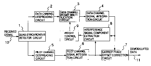
FIG. 1 is a block diagram showing the
configuration of the above described conventional
receiving apparatus. In FIG. 1, numeral 1 denotes a
quasi-synchronous detector circuit for performing
quasi-synchronous detection on a received radio
frequency signal. Numeral 2 denotes a data channel
despreading circuit for performing despreading by using
spreading codes assigned to a data channel. Numeral 4
denotes a data channel signal integration circuit for
integrating a despread data channel signal. Numeral 5
denotes a pilot channel despreading circuit for
performing despreading by using spreading codes
assigned to a pilot channel. Numeral 6 denotes a pilot
channel signal integration circuit for integrating a
despread pilot channel signal. Numeral 7 denotes a
carrier phase offset correction circuit for correcting
_ _ 3 _ 2153617
a carrier phase offset contained in a data channel
signal. Numeral 10 denotes a received signal. Numeral
11 denotes demodulated data.
Operation of the above described conventional
circuit will now be described by referring to FIG. 1.
The received signal 10 is subjected to quasi-
synchronous detection in the quasi-synchronous detector
circuit 1 to produce a baseband signal. This baseband
signal is despread in the data channel despreading
circuit 2. At this time, the despreading is performed
by using a spreading sequence assigned to a data
channel. The despread signal is integrated in the data
channel signal integration circuit 4. By the
despreading operation and integration operation, the
signal of assigned data channel can be extracted. The
integrated signal contains the difference between the
carrier phase of the received signal 10 and the carrier
phase of a local oscillator.
On the other hand, the baseband signal
outputted from the quasi-synchronous detector circuit 1
is despread in the pilot channel despreading circuit 5.
At this time, the despreading is performed by using a
spreading sequence assigned to a pilot channel. The
despread signal is integrated in the pilot channel
signal integration circuit 6. Since a signal known on
the receiving side is inserted in the pilot channel,
the difference between the carrier phase of the
2153617
. - 4 -
received signal 10 and the carrier phase of the local
oscillator can be known.
In the carrier phase offset correction
circuit, demodulated data 11 having a corrected carrier
phase offset can be obtained by using the result of
integration of the data channel signal and the result
of integration of the pilot channel signal thus
obtained.
In the above described conventional receiving
apparatus, however, correlation levels with respect to
other channel components become great because of an
increased number of multiple users and multipath
distortion, resulting in great interference components
contained in the correlatively detected data channel
signal and pilot channel signal. As a result, errors
are caused in demodulated data and the communication
quality is degraded. Also in the case where a narrow
band interference signal is contained in the receceived
signal, interference components contained in the
correlatively detected data channel signal and pilot
channel signal become great, resulting in degradation
in communication quality.
SUMMARY OF THE INVENTION
The present invention solves the above
described problems of the conventional technique. An
object of the present invention is to provide a CDMA
` 2153617
_ - 5 -
receiving apparatus capable of reducing errors of
demodulated data and improving the receiving quality.
In accordance with the present invention, the
receiving apparatus includes means for providing the
signals after despreading with weights and the weights
are adaptively controlled so as to m;n;m; ze the
interference signal component contained in the
correlatively detected signal. Thereby, the
interference signal component can be reduced and the
above described object is achieved.
Owing to this configuration, errors in the
demodulated data are reduced and the communication
quality can be improved. Furthermore, it is also
possible to increase the number of users which can use
the communication while maintaining the communication
quality at substantially the same level. Efficient use
of frequency resources can thus be realized.
BRIEF DESCRIPTION OF THE DRAWING
FIG. 1 is a block diagram of a conventional
CDMA receiving apparatus;
FIG. 2 is a block diagram of a first
embodiment of a CDMA receiving apparatus according to
the present invention;
FIG. 3 is a diagram showing a transmitted
signal of a CDMA transmitting apparatus;
FIG. 4 is a diagram showing a received signal
of a CDMA receiving apparatus;
_ - 6 - 2153617
FIG. 5 iS a block diagram of an interference
signal component extracting circuit of a CDMA receiving
apparatus according to the present invention;
FIG. 6 is a block diagram showing a first
configuration example of a weight control circuit of a
CDMA receiving apparatus according to the present
nventlon;
FIG. 7 iS a block diagram showing a second
configuration example of the weight control circuit of
the CDMA receiving apparatus according to the present
invention;
FIG. 8 iS a diagram showing demodulated data
of a CDMA receiving apparatuse according to the present
invention and a convention CDMA receiving apparatus;
FIG. 9 iS a block diagram of a second
embodiment of a CDMA receiving apparatus according to
the present invention;
FIG. 10 iS a block diagram of an interference
signal component extracting circuit used in the second
embodiment and a third embodiment of a CDMA receiving
apparatus according to the present invention; and
FIG. 11 iS a block diagram of the embodiment
of a CDMA receiving apparatus according to the present
lnvent lon .
DESCRIPTION OF THE PREFERRED EMBODIMENTS
FIG. 2 is a block diagram showing the
configuration of a first embodiment according to the
_ 7 _ 21S3B17
-
present invention. Numericals 1, 2, 4, 5, 6, 7, 10 and
11 shown in FIG. 2 denote the same components as those
of FIG. 1 denoted by like numerals and duplicated
description of them will be omitted. In FIG. 2,
numeral 3 denotes a data channel weight multiplication
circuit for providing despread data channel signals
with weights. Numeral 8 denotes an interference signal
component extraction circuit for extracting the
interference signal component of the data channel from
the correlatively detected signal component. Numeral 9
denotes a weight control circuit for controlling
weights in the data channel weight multiplication
circuit 3 on the basis of the extracted interference
signal component of the data channel.
Operation of the CDMA receiving apparatus
configured as heretofore described will now be
described. If a signal as shown in FIG. 3 is
transmitted by a base station, the received signal 10
shown in FIG. 4 is received by the receiving apparatus.
The received signal 10 is subjected to quasi-
synchronous detection in the quasi-synchronous detector
circuit 1 to produce a baseband signal. This baseband
signal is despread in the data channel despreading
circuit 2. In the signal despread in the data channel
despreading circuit 2, signal components of spreading
channels used by other users and interference signal
components such as signal components of a delayed wave
. 2153617
_ - 8 -
or a lead wave caused by multipath propagation are also
contained besides the signal component of the assigned
spreading channel. Weights in the data channel weight
multiplication circuit 3 are determined so that the
above described interference signal component may be
reduced to the minimum by the integrating operation in
the data channel signal integration circuit 4. In the
output signal of the data channel signal integration
circuit 4, the correlatively detected data channel
signal component and the correlatively detected
interference signal component are contained. In the
interference signal component extraction circuit 8, the
correlatively detected interference signal component is
extracted. In the extracted signal, information of
spreading codes which are being used by other users and
information of multipath propagation path state are
contained.
A configuration example of the interferene
signal component extraction circuit is shown in FIG. 5.
In FIG. 5, numeral 15 denotes a data judgement circuit
for judging an output signal of the data channel signal
integration circuit 4. Numeral 16 denotes an output
signal of the data channel signal integration circuit
4. Numeral 17 denotes a signal obtained after judgement
in the data judgement circuit 15. Numeral 18 denotes
an extracted interference signal component.
In the signal 16, a signal component x(t) of
the assigned channel and an interference component e(t)
` 2153617
g
caused by other channels or multipath are contained.
Therefore, the signal 16 can be represented by the
following equation.
y(t) = x(t) + e(t) (1)
The data judgement circuit 15 forms a hard
decision upon the soft decision value signal 16 and
derives a discrete signal value of the assigned
channel. If this judgement is performed correctly, the
signal 17 becomes equal to x(t). Therefore, the
interference signal component can be derived as
represented by the following equation.
Signal 16 - Signal 17 = y(t) - x(t)
= e(t) (2)
In the output signal of the data channel
signal integration circuit 4, the carrier phase offset
is contained. When the above described judgement is to
be formed, the carrier phase offset information fed
from the pilot channel signal integration circuit 6 is
needed.
By using the interference signal component
thus derived, the weight control circuit 9 derives
optimum weight values for the data channel weight
multiplication circuit 3.
-- - 10 _ 21~3617
The case where minim; zation of the mean
square value of the interference signal component is
used as criterion for deriving the optimum value will
now be described. In the output signal of the data
channel despreading circuit 2, the signal of chip rate
corresponding to data at time nT (where T is the
transmission interval of data) is described by the
following equation.
y1(n) d(n) 1.
YN (n) d(n) eN(n)
In this equation, Yi(n) (i = 1, ..., N)
represents the signal outputted from the data channel
despreading circuit 2 at the chip rate, and d(n)
represents data of the assigned channel. Furthermore,
ei(n) (i = 1, ..., N) represents the interference
signal component, and N represents the spreading ratio.
A signal obtained by multiplying the signal of each
chip rate and the weights wi(n) (i = 1, ..., N) in the
data channel weight multiplication circuit 3 is
expressed by the following equation.
2153617
-- 11 --
yl(n) wl(n) el(n)-wl(n
= d(n) . +
Y N (n) WN (n) e (n)-w (n)
The output signal of the data channel signal
integration circuit 4 is expressed by the following
equation.
N
~ ~
y(n) = ~ Y k (n)
k=l
N N
= d(n) ~ wk(n) + ~ ek(n) wk(
Let an error signal be defined by the
following equation.
(n) = y(n) - d(n) (6)
Supposing that d(n), ei(n) and wi(n) (i = 1,
..., N) are independent of each other and the average
value of d(n) is 0, the mean square value of the error
signal is expressed by the following equation.
- 21~617
-- 12 --
N 2 N 2
E[E2(n)] = E[d2(n)]-E ~ wk(n)-l +E ~ ek(n)-wk(n)
,k=l , ~k=l
(7)
In this equation, E [ ] represents the average value.
This equation forms a surface of second degree in an N-
dimensional space having wi(n) (i = 1, ..., N) as
variables. The weight control circuit 9 derives
weights wi(n) (i = 1, ..., N) min;mi zing the equation
(7). Hereafter, an example of a method of determining
the weights wi(n) (i = 1, ..., N) will be described.
FIG. 6 shows a configuration example of the
weight control circuit 9. In FIG. 6, numeral 19
denotes a correlation function measuring circuit for
deriving a correlation function. Numeral 20 denotes a
weight calculation circuit. The operation principle of
the configuration example shown in FIG. 6 will now be
described. The mean square error expressed by equation
(7) always assumes 0 or a positive value. When this
value becomes its minimum, therefore, the weights wi(n)
(i = 1, ..., N) satisfy the following condition.
aE[e (n)] = o (i = 1 N) (8)
` _ - 13 - 21~3617
By calculating equation (8), we get the
following equation.
N N
5E[d (n)]. ~ E[wk(n)]-l + ~ E[ek(n)-ei(n)-Wk(n)]
= 0 (i = 1, ..., N) (9)
Supposing that wi(n) (i = 1, ..., N) do not depend upon
time n, equation (9) can be written in the following
form.
N
~ Wk(E[d2(n)]+E[ek(n)-el(n)])=E[d (n)] (i = 1,--., N)
(10)
Equation (10) can be represented in a matrix form as
follows:
R11 .. RN1 W.1 d
= ( 1 1 )
R ... R WN - d
where
Rij = E[d(n)] + E[ei(n)-ej(n)] (12)
2153617
- 14 -
Pd = E[d(n)] (13)
From equation (11), we get the following equation.
W.1 R 1 1 RN1 1 d
WN R 1N NN d ( 1 4 )
From equation ( 14 ), the weights wi(n) (i = 1, ..., N)
can be derived. Heretofore, the case where the weights
wi(n) (i = 1, ..., N) do not depend upon n has been
described. Also in the case where the weights depend
upon n, such as the case where the weights vary
periodically, the weights can be derived in the same
way. As heretofore described, the optimum values of
the weights in the data channel weight multiplication
circuit 3 are derived by the calculation of the
correlation function of the interference signal in the
correlation function measuring circuit 19 and the
calculation of the inverse matrix in the weight
calculation circuit 20.
FIG. 7 shows a configuration example of the
weight control circuit 9. In FIG. 7, numeral 21
denotes a mean square error function gradient
calculation circuit for deriving the gradient vector of
` - 15 - 2153617
the mean square error and numeral 22 denotes a weight
update circuit for updating the weight on the basis of
the derived gradient vector. As for the method of
calculating the gradient vector and implementing the
weight updating circuit, there are the steepest descent
method, LMS method, learning identification method, and
RLS method. They are known as algorithms of adaptive
filters. Algorithms of adaptive filters are described
in ~Introduction to adaptive filters~, written by S.
Haykin, translated by Takebe, and published by Gendai
Kogakusha (1987), for example. In these algorithms,
the weights are initialized to have appropriate values
and successively converged to optimum values.
Thus in the above described first embodiment,
errors of demodulated data can be reduced as shown in
FIG. 8 by m;n;m; zing the interference signal in the
data channel.
FIG. 9 is a block diagram showing the
configuration of a second embodiment according to the
present invention. Numericals 1, 2, 4, 5, 6, 7, 10 and
11 shown in FIG. 9 denote the same components as those
of FIG. 2 denoted by like numerals and duplicated
description of them will be omitted. In FIG. 9,
numeral 12 denotes a pilot channel weight multipli-
cation circuit for providing the despread pilot channelsignal with weights. Numeral 13 denotes a pilot
channel interference signal component extraction
_ - 16 - 2153617
circuit for extracting the interference signal
component of the pilot channel from the correlatively
detected pilot channel signal. Numeral 14 denotes a
pilot channel weight control circuit for controlling
weights in the pilot channel weight multiplication
circuit 12 on the basis of the extracted interference
signal component of the pilot channel.
Operation of the CDMA receiving apparatus
configured as heretofore described will now be
described. If a signal as shown in FIG. 3 is
transmitted by a base station, the received signal 10
shown in FIG. 4 is received by the receiving apparatus.
The received signal 10 is subjected to quasi-
synchronous detection in the quasi-synchronous detector
circuit 1 to produce a baseband signal. This baseband
signal is despread in the data channel despreading
circuit 2. At this time, the despreading is performed
by using a spreading sequence assigned to the data
channel. The despread signal is integrated in the data
channel signal integration circuit 4. By the
despreading operation and integration operation
heretofore described, the signal of assigned data
channel can be extracted. The integrated signal
contains the difference between the carrier phase of
the received signal 10 and the carrier phase of the
local oscillator.
On the other hand, the baseband signal
outputted from the quasi-synchronous detector circuit 1
~ - 17 - 2153617
is despread in the pilot channel despreading circuit 5.
In the signal despread in the pilot channel despreading
circuit S, signal components of spreading channels
other than the pilot channel and interference signal
components, such as signal components of a delayed wave
or a preceding wave caused by multipath propagation,
are also contained besides the signal component of the
pilot channel. The weights in the pilot channel weight
multiplication circuit 12 are determined so that the
interference signal component may be reduced to the
minimum by the integrating operation in the pilot
channel signal integration circuit 6. As for the
method of this determination, a concept similar to the
method of mi n i m; zing the interference signal component
in the above described first embodiment is applied to
the pilot channel. Therefore, it is only necessary to
replace the data d(n) by the pilot channel signal p(n).
In the output signal of the pilot channel
signal integration circuit 6, the correlatively
detected pilot channel signal component and
interference signal component are contained. In the
pilot channel interference signal component extraction
circuit 13, the interference signal component is
extracted. The extraction circuit has a configuration
as shown in FIG. 10, for example. In FIG. 10, numeral
23 denotes a smoothing circuit for smoothing an output
signal of the pilot channel signal integration circuit
- 18 - 2153617
-
4 and numeral 24 denotes an output signal of the pilot
channel signal integration circuit 4. Numeral 25
denotes a pilot channel signal after smoothing and
numeral 26 denotes an extracted interference signal
component. In the signal 24 (yp(t)), a signal
component xp(t) of the pilot channel and an
interference signal component ep(t) caused by channels
other than the pilot channel or the multipath are
contained. Therefore, the signal 24 can be expressed
by the following equation.
yp(t) = xp(t) + ep(t) (15)
In the smoothing circuit 23, the signal 24
expressed by equation (15) is smoothed. In the case
where the same data already known by the receiving side
are inserted into the pilot channel, xp(t) is a signal
involving a change close to the carrier frequency
offset. On the other hand, the interference component
ep(t) is a signal having a comparatively wide
bandwidth. Therefore, the interference component ep(t)
is removed by the smoothing circuit 23 and the signal
25 becomes nearly equal to xp(t). Accordingly, the
interference signal component 26 is derived by the
following equation.
Signal 24 - signal 25 = yp(t) - xp(t) (16)
= ep(t)
- 19 _ 2l536l7
-
As another extraction circuit, the
configuration example of the interference signal
component extraction circuit in the first embodiment
can also be applied to the pilot channel. Data of the
pilot channel is already known. In the case where
estimation of the carrier phase offset and amplitude of
the pilot channel is performed correctly, therefore,
the interference signal component can always be
detected accurately.
In the extracted interference signal
component, information of spreading codes of channels
other than the pilot channel and information of
multipath propagation path state are contained. In the
pilot channel weight control circuit 14, optimum values
of the weight in the pilot channel weight
multiplication circuit 2 are derived by using these
kinds of information. As for the method of deriving
the optimum values, the method of deriving optimum
values of the weight for the data channel in the first
embodiment is applied to the pilot channel.
As heretofore described, it is possible in
the second embodiment to improve the estimation
precision of the carrier phase offset and reduce errors
of demodulated data by minimizing the interference
signal component in the pilot channel. Furthermore,
the transmission power of the pilot channel can be
reduced while maintaining the precision of the carrier
21~3617
- 20 -
phase offset nearly at the same level. In addition,
the power consumption can be reduced and interference
for each user can be reduced.
FIG. 11 is a block diagram showing the
configuration of a third embodiment according to the
present invention. Numericals 1 through 14 shown in
FIG. 11 denote the same components as those of FIGS. 2
and 9 denoted by like numerals. Since the
configuration of the present embodiment is a
combination of the first embodiment and the second
embodiment, detailed description of the configuration
will be omitted.
In output signals of the data channel signal
integration circuit 4 and the pilot channel signal
lS integration circuit 6, interference components
concerning the data channel and the pilot channel are
respectively minimized as disclosed in the first
embodiment and the second embodiment, respectively.
Thus errors in demodulated data derived from these
signals can be reduced.
As heretofore described, the present
invention realizes an excellent CDMA receiving
apparatus capable of improving the receiving quality by
providing a circuit for providing signals after
despreading with weights and by controlling the weights
adaptively so as to minimize the interference signal
component contained in the correlatively detected
slgnal .