Note: Descriptions are shown in the official language in which they were submitted.
- 21~37Sl
DEMODULATOR CAPABLE OF IMPROVING A SYMBOL ERROR RATE
WITHOUT DECREASING A TRANSMISSION RATE
Background of the Inventlon:
This lnvention relates to a demodulator for
demodulatlng a recelved slgnal lnto a demodulated slgnal
by dlfferential detectlon.
It is known in the art that a demodulator
demodulates a received signal into a demodulated signal
by differential detection. Such a demodulator may be
used in a mobile communication system. The received
signal is transmitted as a transmission signal from a
transmitter. For example, the transmission signal is
produced by differential phase shift keying in the
transmitter. In this case, the transmission signal has
phase information.
A conventional demodulator comprises a phase
variation producing sectlon and a demodulator section.
The phase variation producing section is supplied with
the received signal and produces a phase variation signal
representative of a phase variation between an
instantaneous phase based on the phase information and a
phase offset determined by the demodulator. The phase
variation signal is supplied to the demodulator section.
-- 21S3761
The demodulator sectlon glves a predetermined
delay time to the phase variation signal to produce a
delayed phase variation signal. Furthermore, the
demodulator section carries out differential detection in
accordance wlth the phase variation signal and the
delayed phase varlation signal to produce the demodulated
signal.
Inasmuch as differential detection is carried out
in accordance with the phase variation signal and the
delayed phase variation signal in the conventional
demodulàtor, a symbol error rate increases in comparison
with coherent detection. In order to improve the symbol
error rate in the conventional demodulator, it is
necessary to produce the transmission signal in using an
error-correcting code.
However, transmission rate is decreased on using
the error-correcting code as known in the art.
Furthermore, it is necessary for the transmitter to have
a coding circuit for carrying out error correction coding
algorithm. In addition, it is necessary for the
conventional demodulator to have a decoding circuit for
carrying out decoding. Namely, not only the transmission
rate decreases but also demodulator must have a complex
structure on using the error-correcting code.
Summary of the Invention:
It is therefore an object of this invention to
provide a demodulator capable of improving a symbol error
rate without reducing a transmission rate.
- 2153761
It is another object of this invention to provide
a demodulator having a simple structure.
Other ob~ects of this invention will become clear
as the description proceeds.
On describing the gist of this invention, it is
possible to understand that a demodulator is supplied
with a modulated signal having phase information as a
received signal for demodulating the received signal into
a demodulated signal by differential detection.
According to a first aspect of this invention,
the demodulator comprises delay means supplied with an
input signal based on the received signal for delaying
the input signal to produce first through N-th delayed
signals which have first through N-th delayed times
different from one another, where N represents an odd
number which is not less than three, first producing
means for carrying out the differential detection in
accordance with the input signal and the first through
the N-th delayed signals to produce first through K-th
output signals, where K represents a positive integer
equal to (N+1)/2, the first producing means recursively
repeating the differential detection until the positive
integer K is equal to two and producing first and second
output result signals, and second producing means for
producing the demodulated signal in accordance with the
first and the second output result signals.
According to a second aspect of this invention,
the demodulator comprises delay means supplled with an
- 2153761
lnput signal based on the received signal for delaying
the input signal to produce first through third delayed
slgnals which have first through third delayed times
different from one another, differential detecting means
for carrying out differential detection in accordance
with the input signal and the first through the thlrd
delayed signals to produce flrst and second output
signals, first correcting means for correcting the first
delayed signal in accordance with the first output signal
to produce a first corrected signal, second correcting
means for correcting the second delayed signal in
accordance with the second output signal to produce a
second corrected signal, and producing means for
producing the demodulated signal in accordance with the
first and the second corrected signals.
According to a third aspect of this invention,
the demodulator comprises delay means supplied with an
input signal based on the received slgnal for delaylng
the input slgnal to produce flrst through fifth delayed
signals which have first through fifth delayed times
different from one another, first differential detectlng
means for carrylng out differential detection in
accordance with the lnput slgnal and the flrst through
the fifth delayed signals to produce first through third
output signals, first correcting means for correcting the
first delayed signal in accordance with the first output
signal to produce a first corrected signal, second
correcting means for correcting the second and the third
215 3 76i
delayed signals in accordance with the second output
signal to produce second and third corrected signals,
third correcting means for correcting the fourth delayed
signal in accordance with the third output signal to
produce a fourth corrected signal, second differential
detecting means for carrying out dlfferential detection
in accordance with the first through the fourth corrected
signals to produce fourth and fifth output signals,
fourth correcting means for correcting the second
corrected signal in accordance with the fourth output
signal to produce a fifth corrected signal, fifth
correcting means for correcting the third corrected
signal in accordance with the fifth output signal to
produce a sixth corrected signal, and producing means for
producing the demodulated signal in accordance with the
fifth and the sixth corrected signals.
Brief Description of the Drawings:
Fig. 1 is a block diagram of a conventional
demodulator;
Fig. 2 ls a block dlagram of a demodulator
according to a first embodiment of this invention; and
Flg. 3 is a block diagram of a demodulator
according to a second embodiment of this invention.
Description of the Preferred Embodiments:
Referrlng to Fig. 1, description will first be
made as regards a conventional demodulator 10 for a
better understanding of this inventlon. The demodulator
10 ls supplled wlth a modulated signal as a received
~ 1 ~ 3 7 ~ 1
signal whlch is transmltted from a transmltter (not
shown). For example, the modulated signal is produced by
differential quadrature phase shift keylng (DQPSK) ln the
transmitter. In this case, the modulated signal has
phase lnformation. The demodulator 10 is operable to
demodulate the received signal lnto a demodulated slgnal
by dlfferential detection.
The demodulator 10 comprlses a phase varlatlon
produclng sectlon 11 and a demodulator sectlon 12.
Supplled wlth the recelved slgnal, the phase varlatlon
produclng sectlon 11 produces a phase varlation signal
representatlve of a phase varlatlon between an
lnstantaneous phase based on the phase lnformatlon and a
phase offset determlned by the demodulator 10.
More partlcularly, lt wlll be assumed that the
phase lnformation represents four phase positlons apart
from each other by ~ /4 radlans (on I-Q slgnal space).
The phase offset determlned by the demodulator 10 may
represent a flxed phase posltlon. The phase varlation
produclng sectlon 11 compares each of phase posltlons
wlth the flxed phase posltlon to produce the phase
varlatlon slgnal.
The phase varlatlon slgnal ls supplled to the
demodulator sectlon 12 to be sub~ected to dlfferentlal
detectlon. The demodulator sectlon 12 comprlses a delay
clrcult (D) 13, a subtracter clrcult 14, and a data
judglng clrcult (DET) 15. The delay clrcult 13 glves a
predetermlned delay tlme to the phase variatlon slgnal to
21S~761
produce a delayed phase varlation signal. The
predetermined delay time may be equal to a time duration
of a symbol.
Supplied wlth the phase variation signal and the
delayed phase variation signal, the subtracter clrcuit 14
subtracts the delayed phase variation signal from the
phase variation signal to produce a phase difference
signal having a difference level representatlve of a
phase difference between the phase varlation signal and
the delayed phase variatlon signal. Namely, the
subtracter circuit 14 carries out differential detection
in accordance with the the phase variation signal and the
delayed phase variation signal to produce the phase
difference signal.
The phase difference signal is supplied from the
subtracter circuit 14 to the data ~udging circuit 15.
The ~udging circuit 15 ~udges which phase difference
level among all of modulated phase difference levels is
the most like with the difference level of the phase
difference signal to produce the demodulated signal as
known in the art.
By the way, a symbol error rate increases in
comparison with coherent detection inasmuch as
differential detection is carried out in accordance with
the phase variation signal and the delayed phase
variation signal in the demodulator 10. In order to
improve the symbol error rate in the demodulator 10, it
is necessary to produce the transmission signal in using
21S3761
an error-correcting code.
However, transmission rate is decreased on using
the error-correcting code as known in the art.
Furthermore, lt is necessary for the demodulator 10 to
have a decoding clrcuit for carrylng out decodlng.
Namely, not only the transmisslon rate is decreased but
also demodulator 10 must have a complex structure on
using the error-correcting code.
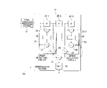
Referrlng to Fig. 2, description will proceed to
a demodulator according to a first embodiment of this
invention. The illustrated demodulator is different in
structure from the demodulator 10 described in
con~unction with Fig. 1 and is therefore designated
afresh by a reference numeral 20. The demodulator 20
comprises the phase variation producing section 11
described in conjunction with Fig. 1 and a demodulator
sectlon 21 different in structure from the demodulator
section 12 illustrated in Fig. 1. The demodulator
section 21 comprises similar parts which are designated
by like reference numerals and are operable with likewise
named signals.
The demodulator section 21 comprises first
through N-th delay circuits 22-1 to 22-N, where N
represents an odd number which is not less than three.
In the example being illustrated, the odd number N is
equal to three. Each of the first through the third
delay circuits 22-1 to 22-3 gives a delay of a
predetermined time to a signal supplied thereto. The
21537~1
first through the third delay circuits 22-1 to 22-3
produce flrst through third delayed slgnals,
respectively. More particularly, the first through the
third delay circuits 22-1 to 22-3 produce first through
third delayed phase variatlon signals, respectively.
The demodulator section 21 further comprlses
flrst through K-th prlmary subtracter circults 23-1 to
23-K, where K represents a positive integer equal to
(N+1)/2. When the odd number N ls equal to three, the
posltive integer K is equal to two. Supplied wlth the
phase variation signal and the first delayed phase
variation signal, the first primary subtracter circult
23-1 subtracts the first delayed phase variation signal
from the phase variation signal. More partlcularly, the
flrst primary subtracter circuit 23-1 calculates a first
phase difference between the first delayed phase
varlatlon slgnal and the phase varlatlon slgnal to
produce a first phase difference signal representative of
the first phase difference. Similarly, the second
prlmary subtracter clrcuit 23-2 calculates a second phase
dlfference between the second delayed phase varlatlon
signal and the third phase variation signal to produce a
second phase difference signal representative of the
second phase difference. The flrst and the second phase
dlfference slgnals may be called flrst and second output
slgnals, respectlvely.
The flrst and the second phase difference signals
are supplied to first and second correcting circuits 24
21~3~61
and 25. The first correcting clrcuit 24 corrects the
flrst delayed phase variation signal in accordance with
the flrst phase dlfference signal to produce a flrst
corrected phase signal whlch may be called a first output
result slgnal. Simllarly, the second correctlng clrcult
25 corrects the thlrd delayed phase varlatlon slgnal ln
accordance wlth the second phase dlfference slgnal to
produce a second corrected phase slgnal whlch may be
called a second output result slgnal.
More speclfically, the flrst correctlng clrcult
24 comprlses a flrst error detecting clrcult (MOD) 26, a
flrst multlplier circult 27, and an adder clrcult 28.
The flrst error detecting circult 26 ls supplled wlth the
flrst phase dlfference slgnal and detects a flrst phase
error between the flrst phase dlfference and an ldeal
phase dlfference based on a tentatlve demodulated slgnal
to produce a flrst phase error slgnal representatlve of
the flrst phase error.
Supplled wlth the flrst phase error slgnal, the
flrst multlpller clrcult 27 multlplles the flrst phase
error slgnal by a predetermlned coefficlent PC to produce
a flrst multlplled slgnal. The predetermined coefficient
PC may represent a value between zero and one (both
excluslve). The adder clrcult 28 calculates a sum of the
first multiplled signal and the first delayed phase
varlatlon signal to produce the first corrected phase
signal.
ll 2153761
The second correcting circuit 25 comprises a
second error detecting circuit (MOD) 29, a second
multiplier circuit 30, and a subtracter circuit 31. The
second error detecting circuit 29 is supplied with the
second phase difference signal and detects a second phase
error between the second phase dlfference and an ldeal
phase difference based on a tentative demodulated signal
to produce a second phase error signal representative of
the second phase error.
Supplled with the second phase error signal, the
second multiplier circuit 30 multiplies the second phase
error signal by a predetermined coefficient PC2 (0 < PC2
< 1) to produce a second multiplied signal. The
subtracter circuit 31 subtracts the second multiplied
signal from the second delayed phase variation signal to
produce the second corrected phase signal.
The first and the second corrected phase signals
are supplied to the main subtracter circuit 14. The main
subtracter circuit 14 subtracts the second corrected
phase signal from the first corrected phase signal to
produce the phase difference signal having the phase
difference level. The phase difference signal is
delivered to the data ~udging circuit 15. The data
judglng clrcult 15 judges whlch phase difference level
among all of modulated phase difference levels is the
most like with the phase difference level of the phase
difference signal to produce the demodulated signal.
`~ 2153761
12
As readily understood from the above description,
the flrst and the second primary subtracter circuits 23-1
and 23-2 and the first and the second correcting circuits
24 and 25 are collectively operable as a flrst producing
section for carrying out the differential detection in
accordance with the phase variation signal and the first
through the third delayed phase variation signals to
produce first and second output result signals. When the
demodulator section 21 comprises the first through the
N-th delay circuits 22-1 to 22-N, the first producing
section carries out the differential detection in
accordance with the phase variation signal and the first
through the N-th delayed phase variation signals until
the positive integer K is equal to two.
Referring to Fig. 3, description will proceed to
a demodulator according to a second embodiment of this
invention. In the illustrated example, the odd number N
is equal to five and the positive integer K is equal to
three. The illustrated demodulator is different in
structure from the demodulator 20 described in
con~unction with Fig. 2 and is therefore designated
afresh by a reference numeral 40. The demodulator 40
comprises the phase variation producing section 11
described in con~unction wlth Fig. 1 and a demodulator
section 41 different in structure from the demodulator
section 21 illustrated ln Fig. 2. The demodulator
section 41 comprises slmilar parts which are designated
by like reference numerals.
2153761
13
The demodulator section 41 comprlses the first
through the flfth delay circuits 22-1 to 22-5. The first
through the fifth delay circuits 22-1 to 22-5 produce the
first through the fifth delayed phase variation signals,
respectively.
The demodulator section 41 comprises the first
through the third primary subtracter circuits 23-1 to 23-
3. The first through the thlrd primary subtracter
circuits 23-1 to 23-3 produce the first through the third
phase difference signals, respectively.
As described in conjunction with Fig. 2, the
first correcting circuit 24 produces the first corrected
phase signal in accordance with the first phase
difference signal and the first delayed phase variation
signal.
The second correcting circuit 25 illustrated in
Fig. 3 is different in structure from the second
correcting circuit 25 illustrated in Fig. 2. In Fig. 3,
the second correcting circuit 25 further comprises an
adder circuit 42. The adder circuit 42 calculates a sum
of the second multiplied signal and the third delayed
phase variation signal to produce a sum signal as a third
corrected phase signal.
The third phase difference signal is supplied to
a third correcting circuit 43 which is similar in
structure to the second correcting circuit 25 illustrated
in Fig. 2. The third correcting circuit 43 comprises a
third error detecting circuit 44, a third multiplier
21S3761
14
clrcuit 45, and a subtracter circuit 46. The third
correcting circuit 43 produces a fourth corrected phase
signal in accordance with the third phase difference
signal and the fourth delayed phase variation signal.
The demodulator section 41 further comprises
first and second subsidiary subtracter circuits 47 and
48. Supplied with the first and the second corrected
phase signals, the first subsidiary subtracter circuit 47
subtracts the second corrected phase signal from the
first corrected phase signal to produce a fourth phase
difference signal. More particularly, the first
subsidiary subtracter circuit 47 calculates a fourth
phase difference between the first and the second
corrected phase signals to produce the fourth phase
difference signal representative of the fourth phase
difference.
Similarly, the second subsidiary subtracter
circuit 48 subtracts the fourth corrected phase signal
from the third corrected phase signal to produce a fifth
phase difference signal representative of a fifth phase
difference.
The fourth phase difference signal is supplied
with a fourth correcting circuit 49. Furthermore, the
second corrected phase signal is supplied with the fourth
correcting circuit 49. The fourth correcting circuit 49
is similar in structure to the first correcting circuit
24. The fourth correcting circuit 49 comprises a fourth
phase error detecting circuit 50, a fourth multiplier
- 2153761
circuit 51, and an adder circuit 52 and produces a flfth
corrected phase signal in accordance with the fourth
phase difference signal and the second corrected phase
signal.
The fifth phase difference signal is supplled
with a fifth correcting circuit 53. Furthermore, the
third corrected phase signal is supplied with the fifth
correcting circuit 53. The fifth correcting clrcult 53
ls slmllar ln structure to the thlrd correctlng clrcult
43. The flfth correctlng clrcult 53 comprises a fifth
phase error detectlng clrcult 54, a flfth multlpller
clrcult 55, and a subtracter circult 56 and produces a
slxth corrected phase slgnal ln accordance wlth fifth
phase dlfference slgnal and the thlrd corrected phase
slgnal.
Supplled wlth the flfth and the slxth corrected
phase slgnals, the maln subtracter clrcult 32 calculates
the maln phase dlfference between the flfth and the six
corrected phase signals to produce the main phase
differencè signal representative of the main phase
difference having the maln phase dlfference level.
As described ln con~unction wlth Fig. 2, the data
judging circuit 33 produces the demodulated signal on the
basls of the maln phase dlfference slgnal.
As readlly understood from the above descrlptlon,
the flrst through the thlrd prlmary subtracter clrcuits
23-1 to 23-3, the first through the fifth correcting
clrcults, and the flrst and the second subsldlary
2153761
16
subtracter clrcuits are collectively operable as the
first producing section for carrylng out the differentlal
detection in accordance with the phase varlation signal
and the first through the fifth delayed phase variation
signals to produce first through fourth output signals.
The first producing sectlon recurslvely repeats the
dlfferentlal detectlon untll posltlve lnteger K ls equal
to two.