Note: Descriptions are shown in the official language in which they were submitted.
FIXED-INTERVAL TIMING CIRCUIT AND METHOD
Background Of The Invention
Almost invariably, the operation of digital electronic circuitry requires the
availability or generation of a pulse or delay having a reliable and
consistent duration.
Individual devices, especially those fabricated upon high-density integrated
circuits cannot
usually be relied upon to provide accurate or consistent time delays or clock
functions. This
is because, barring the use of prohibitively expensive methods (such as
trimming), fabrication
process tolerances cannot be tightly controlled for the batch-production
environments in which
such circuits are typically manufactured. For example, in the mass-production
of
semiconductor integrated circuits it is not uncommon for absolute individual
device
characteristics, such as the particular channel resistance within a field-
effect transistor ("FET")
or a given device capacitance level, to vary by as much as 100 percent from
wafer to wafer.
It is this wide variation in device characteristics that renders individual
passive or active
devices upon an integrated circuit impractical and unreliable for purposes of
providing
predictable timing intervals -- especially in high-speed computing
applications where accurate
timing and precise circuit delay times are critical.
Summary Of The Invention
The aforementioned problems are solved, in accordance with the principles of
the invention, by providing a system and method for generating a signal having
a reliable,
fixed duration and/or delay as a function of relative, not absolute, device
characteristics. That
is to say, the time period of the generated signal is determined as a ratio of
one device's
operating characteristics to another device's operating characteristics. In
particular, the
invention provides a fixed time signal or delay as a function of the relative
values of two
capacitive elements that have a known ratio of capacitance with respect to
each other. The
invention is particularly useful when implemented upon an integrated circuit,
as standard
fabrication techniques for such circuits allow relative device characteristics
to be held to
relatively tight tolerances.
CA 02154703 1998-11-30
- la -
In accordance with one aspect of the present invention a circuit for defining
a
fixed interval, comprising: a first capacitor; a first switch configured to
alternately charge
and discharge said first capacitor at frequency f~; means connected to sense
the effective
resistance of said first capacitor at frequency f~, and responsively bias a
transistor so that
its effective resistance is maintained at a level substantially equal to that
of said sensed
effective resistance of said first capacitor; a second capacitor charged to a
first level; a
second switch configured to switchably discharge said second capacitor via
said biased
transistor; and means for generating a signal having a fixed duration as a
function of the
rate at which said charge upon said second capacitor discharges through said
biased
transistor.
In accordance with yet aspect of the present invention there is provided a
circuit
for defining a fixed interval, comprising: a first capacitor; a first switch
configured to
alternately charge and discharge said first capacitor at frequency f~; means
connected to
sense the effective resistance of said first capacitor at frequency f~, and
responsively bias a
transistor so that the resistance of said transistor is maintained at a level
substantially equal
to that of said sensed effective resistance of said first capacitor; a second
capacitor charged
to a first voltage level; a second switch configured to switchably discharge
said second
capacitor via said biased transistor; means for sensing a voltage evident
across said second
capacitor; and means for providing an indication of the interval over which
said sensed
voltage decays from said first voltage level to a predetermined second voltage
level for
defining the fixed interval.
In accordance with still yet another aspect of the present invention there is
provided a circuit for defining a fixed interval, comprising: a first
capacitor; a first switch
configured to alternately charge and discharge said first capacitor at
frequency f~;
comparator connected to sense the effective resistance of said first capacitor
at frequency
f~, and responsively bias a pair of field-effect transistors so that the
channel resistance of
each said field-effect transistors is maintained at a level substantially
equal to that of said
sensed effective resistance of said first capacitor; a second capacitor
charged to a first
voltage level; a second switch configured to switchably discharge said second
capacitor via
the channel of one of said biased field-effect transistors; means for sensing
a voltage
evident across said second capacitor; and means for providing an indication of
the interval
over which said sensed voltage decays from said first voltage level to a
predetermined
second voltage level for defining the fixed interval.
-2-
Brief Description Of The Drawing
In the drawing:
FIG. 1 shows a schematic illustration of a timing circuit incorporating an
embodiment of the invention;
FIG. 2 provides an illustration of various signal waveforms that occur within
the circuit of FIG. 1; and
FIG. 3 shows a schematic illustration of a simplified equivalent circuit for
the
timing circuit of FIG. 1.
Detailed Description
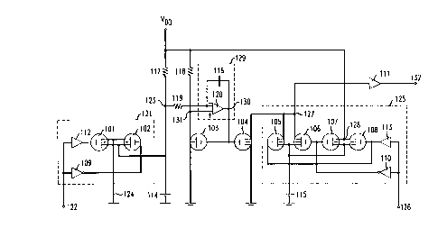
FIG. 1 is an illustration providing a schematic diagram of a timing circuit
incorporating an embodiment of the invention. The circuit is fabricated upon a
single
integrated circuit and includes FETs 101-108, inverters 109-110, buffers 111-
113, reference
capacitor 114, delay capacitor 115, feedback capacitor 116, resistors 117-119,
and operational
amplifier 120. FETs 103 and 104 are a matched pair (i.e., they are fabricated
to exhibit
practically identical electrical characteristics). Likewise, resistors 117 and
118 are also
fabricated to be a matched pair. Ideally, to minimize switching noise, FETs
101 and 102
should have identical channel dimensions. Similarly, the size of the channels
in FETs 105-108
should also be matched.
FETs 101 and 102, along with inverter 109 and buffer 112 (a collection of
components herein after referred to as FET switch 121) are configured to
effectively operate
as a single-pole, single-throw switch that, in response to a reference clock
signal applied to
terminal 122, alternately connects and disconnects one terminal of reference
capacitor 114 and
circuit node 123 to ground terminal 124. When the reference clock signal is in
a low state
(referred to as a logical 0 state) FET switch 121 provides a conductive path
between reference
capacitor 114 and ground terminal 124. Similarly, FETs 105, 106, 107 and 108,
along with
inverter 110 and buffer 113 (collectively referred to as FET switch 125) are
configured to
effectively operate as a single-pole, double-throw switch that, in response to
a trigger signal
applied to terminal 126 alternately connects one terminal of delay capacitor
115 to either
circuit node 127 or circuit node 128. When the reference clock signal is in
high state (referred
to as logical 1 state) a conductive path between delay capacitor 115 and node
127 is created,
and when the reference clock signal is in logical 0 state a conductive path
between reference
~I54 703
-3-
capacitor 114 and node 128 is created.
The circuitry illustrated in FIG. 1 operates as follows. A reference clock
signal,
having a frequency f~, is provided to terminal 122 from a stable source such
as quartz crystal
or other electronic oscillator having a 50% duty cycle. For electrical signals
having a
frequency much less than f~, reference capacitor 114 will appear as a fixed
resistance of value
~ef~ where Rref = 1/(BC~eff~), and C~ef 1S the capacitance of reference
capacitor 114.
Unfortunately, because absolute component values cannot be held to very tight
tolerances upon
the typical integrated circuit, and because the value of 1/(BC~eff~) is only
valid for signals
having a frequency much less than f~ or electrical transients having a time
scale much longer
than 1/f~, the particular resistance value apparent across reference capacitor
114 cannot be
directly relied upon to provide a basis for the generation of a fixed time
signal or delay.
Instead, the circuit of FIG. 1 provides a fixed duration pulse or delay as a
function of the ratio
of the value of reference capacitor 114 (C~ef) and delay capacitor 115
(Cden,.) -- ale typical
integrated circuit fabrication methods make precise control of absolute device
values difficult,
the relative device values upon the wafer can be accurately maintained.
The voltage evident at node 123 has the same frequency as the reference clock
signal. This time dependent signal is time-averaged over a period much longer
than 1/f~ by
low-pass comparator 129 (comprising input resistor 119, feedback capacitor
116, and
operational amplifier 120). The output of low-pass comparator 129 is evident
at node 130 and
serves to bias the gates of FETS 103 and 104. When the voltage evident at node
123 is
greater than the voltage evident at node 131 the output of low-pass comparator
129 is reduced.
This reduced voltage is applied to the gate of FET 103, and results in an
increase of the
effective channel resistance of FET 103. Consequently, the voltage evident at
node 131 is
increased. Conversely, when the voltage evident at node 123 is less than the
voltage evident
at node 131, the output of low-pass comparator 129 is increased, thereby
lowering the
effective channel resistance of FET 103, and causing the voltage at node 131
to decrease. The
voltage at node 123 is given by:
__ Rref
V123 vDD
8117 +Rref ) .
Similarly, the voltage evident at node 131, V,3,, is a function of the
relative values of the FET
103's effective channel resistance, R,o3, and resistor 118, R"g. This voltage,
V,3, will be equal
to:
~~~~70~
-4-
__ Rlo3
V131 VDD
C Rlla+Rlo3 ) .
Through the operation of low-pass comparator 129 the voltage applied to the
gate of FET 103
will be adjusted until an equalized state where Rre~R,o3 and V,z3-V,3, is
attained (where V,23
is the time averaged value of V,23). Because FET 103 and FET 104 are a matched
pair, and
both subjected to the same gate voltage, the effective channel resistance of
FET 104, R,o4, will
be equalized with that of FET 103 (R,o3), so that:
1
-Rref-8103 -8104 '
8 C'reffc
Assuming resistor 117 and resistor 118 are each fabricated to have values
approximately three
times that of 1/(BCreff~), it follows that when the reference clock signal is
in a logical 1 state,
the level of V,23 will rise to a maximum value of approximately 1/4VDD. As the
reference
clock signal oscillates, V,23 rises and falls in accordance with the time
constant of the circuit
formed by resistor 117 and delay capacitor 114, the voltage evident at node
131 is held to a
constant value of V,z3. FIG. 2 provides an illustration of various signals
that occur within the
circuit of FIG. 1 during normal operation, including the reference clock
signal (201 ) and the
waveform evident at nodes 123 (202) and 130 (203).
FIG. 3 is a schematic illustration of an equivalent circuit for the timing
circuit
of FIG. 1. As shown, the combination of FET switch 121 and reference capacitor
114 are
represented by resistor 314 (having a value Rref). FET switch 125 is
represented as a single-
pole, double-throw relay controlled by the trigger signal. Matched FETs 103
and 104 are
depicted as resistors 303 and 304, respectively (having the values R,o3 and
R,o4, where
R,o3-R,oa)~ The dotted line connecting the output of operational amplifier 120
with resistors
303 and 304 is a representation of the voltage equalization performed by low-
pass comparator
129.
To initiate the operation of the circuit illustrated in FIGS. 1 and 3, the
trigger
signal applied to terminal 126 is brought from a logical 0 state to a logical
1 state (shown to
occur at time to in FIG. 2). In order to ensure a reliable output by the
circuit of FIGS. 1 and
3 the particular instant at which the trigger signal makes the transition need
not be
synchronized with respect to any transition in signal level by the reference
clock, or the signal
evident at node 122. Furthermore, the period over which the trigger signal is
held in a logical
1 state (tf- to as shown by waveform 204 in FIG. 2) is also inconsequential
with respect to the
70
-5-
generation of fixed time signal or delay by the circuit (except for the
obvious limitation that
the interval t~to have a longer duration than TfX, the signal that will be
output by the circuit
of FIGS. 1 and 3 at terminal 132).
When the trigger signal is at a logical 0 level, a conductive path between
delay
capacitor 115 and VDp is established within FET switch 125. When the reference
clock signal
is brought to a logical 1 level, FET switch 125 provides a conductive path
between delay
capacitor 115 and node 127, thereby allowing delay capacitor 115 to discharge
to ground via
FET 104. As shown by waveform 205 in FIG. 2, the voltage at node 127 initially
rises from
zero to approximately VDD at time t, in response to the trigger signal being
brought to a logical
1 level at to. The delay from to to t~ is a result of the delays introduced by
inverter 110 and
buffer 113 (FIG. 1). The rise of the voltage at node 127 causes the output of
buffer 111
(evident at terminal 132 of FIGS. 1 and 3) to assume a logical 1 level at t2
(see waveform 206
of FIG. 2). The delay from tl to tz is a function of the response time of
buffer 111.
The voltage at node 127 then decays to zero as delay capacitor 115 discharges
through FET 104. The rate of this decay is dictated by the time constant TD,
where TD =
(CdelayR104O ~d
V127 ~ t~ VDD ~ a t/Tp\
Since the value of FET 104's channel resistance, R~o4, is equal to
1/(BC~eff~), it is clear that this
voltage decay is a function of the values of the reference and delay
capacitors:
V127 ~ t~ =VDD ~ g-t/To\
tl (Cdelay-104~
127 DD
( _( 8Creffct)) .
v127 ~ t~ -vDD a Cdelay
At time t3 the voltage level at node 127 falls below the threshold voltage,
V~" of buffer 111
(the output of buffer 111 is 1 for V>V~" and 0 for V<V~. As a result, the
output of buffer
111 assumes a logical 0 level at time t4 (the delay from t3 to t4 being a
function of buffer
111's response time).
The fixed duration, TfX, of the signal provided by the circuit illustrated in
FIGS.
1 and 3 is the time from t2 to time t4, and can be defined as the time it
takes for the voltage
at node 127 to decay from VDD to V~" and can be represented as:
215 ~fl3
-6-
__ Cdelay _ Vth
Tfix ~ 8Czeffctl\ In ~ VDDll .
As VDD, V~," and f~ are known, fixed values, the only true variable in
determining the duration
of TfX is Cref~Cdelay As standard integrated circuit fabrication techniques
allow relative device
characteristics to be held to tight tolerances, the circuitry of FIG. 1, when
implemented upon
an integrated circuit, will reliably and accurately provide a signal defining
a fixed interval.
The invention illustrated in FIGS. 1 and 3 can also be utilized to provide a
fixed delay. The trailing edge of the pulse in waveform 206 (FIG. 2) will
always be delayed
by exactly (TfX+K) from time to (the time at which the trigger signal made the
transition from
logical 0 to logical 1 ). K is the total delay introduced by the operation of
low-pass comparator
129, buffers 111-113, and inverters 109 and 110. K is a constant for a
particular circuit, and
can be readily computed (based upon the physical characteristics of the
particular devices in
the circuit) or measured.
It will be understood that the particular method and embodiment described
above are only illustrative of the principles of the present invention, and
that various
modifications could be made by those skilled in the art without departing from
the scope and
spirit of the present invention, which is limited only by the claims that
follow. One such
modification would be employing an inductor, or other reactive circuit element
in place of the
timing capacitor and/or the reference capacitor.