Note: Descriptions are shown in the official language in which they were submitted.
-1- 21 54g2~
QUANTUM WELL INFRARED FILTER
BACKGROUND OF T~E INVENTION
This invention relates to infrared filters,
and, more partlcularly, to a tunable lnfrared fllter
uslng no moving parts.
In some applications, a sensor (consisting of
a detector, optics, and electronics) is used to
lmage or analyze a scene. Most scenes that are
vlewed by a sensor present a spectrum of wavelengths
Of radiation. It is often desirable to base the
sensor analysis on only some components of the
spectrum, such as a particular band within the
infrared portion of the spectrum.
In some applications the wavelengths of
interest to be sensed may change with time. A
multispectral sensor system is therefore needed to
permit selection of the wavelength being analyzed.
In one approach, the detector itself could be made
controllably sensltive to particular components of
the spectrum. ~owever, a multispectral detector for
the infrared is e2pensive and requires the
development of electronic detector and readout
technology that does not as yet exist. In another
approach, multiple sensors can be used, each sensor
being most sensitlve to a single wavelength band.
In yet another approach, a filter placed
between the scene and the detector ls used to
selectlvely pass a particular band of wavelengths of
radiation of the spectrum. The filter attenuates
all components of the spectrum except for those that
are to be analyzed. A less comple~ broadband sensor
can therefore be used.
Various types of filters are known in the
21 ~ 82~
art. To achieve selectlvity of the wavelength to be
passed by the fllter, lt ls common practlce to
utlllze a multipart fllter, each part passing a
slngle wavelength band. The usual structure of a
multipart filter is a filter wheel, with discrete
filtering regions positloned around the
clrcumference of the wheel. The wheel is rotated to
place the desired filter between the scene and the
detector. The filter wheel tends to be large,
heavy, and cumbersome. It ls therefore not
preferred where the entlre sensor system must be
small and lightweight.
There is a need for an improved filter, for
use in a sensor system, which is controllable to
permit only a selected wavelength range to be
passed. The filter should be small and light in
welght, and have no movlng parts that require
activatlon, consume large amounts of power, or might
be sub~ect to mechanlcal fallure. The present
invention fulfills this need, and further provides
related advantages.
SUMMARY OF THE INVENTION
The present invention provides a controllable
infrared filter and sensor system, and a method for
their fabrication and use. The filter has no moving
parts, and ls small and lightweight. The filter is
activated electrically or optically, rather than
mechanically. The filter can be full~ transparent
or pass only particular wavelengths. The
wavelengths to be passed are selected electrically.
In accordance with the invention, a
controllable infrared filter comprises a quantum
well filter unit operable to absorb infrared energy
21~8~4
at a selected wavelength. The quantum well filter
unlt has a quantum well layer made of an lnfrared
transparent semiconductor material, a flrst barrier
layer made of a second infrared transparent
semiconductor materlal epita~ially contactlng a
first slde of the quantum well layer and having a
flrst barrier layer thlckness, and a second barrier
layer made of a third lnfrared transparent
semlconductor materlal epltaxlally contacting a
second side of the quantum well layer and having a
second barrier layer thlckness.
The fllter also has means for controllably
lntroducing charge carrlers into the quantum well
layer. The charge carrlers can be introduced by
providing a first doped cladding layer in contact
with the first barrler layer on a contact side
remote from the quantum well lager and a second
doped cladding layer ln contact wlth the second
barrier layer on a contact side remote from the
quantum well layer, wherein the flrst barrler layer
thickness is less than the second barrier layer
thickness. There ls a means for controllably
applying a voltage between the first doped cladding
layer and the second doped cladding layer.
Alternatively, the charge carriers can be introduced
b~ a laser having a beam controllably directed into
the quantum well layer, with the laser operating at
a beam wavelength that creates charge carriers in
the quantum well layer.
The filter also includes means for directing
infrared radiation through the first barrier layer,
the quantum well layer, and the second barrier
layer. Such means for directing can include a lens
or mirror system.
When few charge carriers are present in the
quantum well, the quantum well fllter unit passes
- 21~824
all components of the infrared spectrum. When
charge carriers are present ln the quantum well due
to appllcation of an electrlcal voltage or
introduction of laser light, the quantum well fllter
unit absorbs a portlon of the spectrum determined b~
the dimensions of the quantum well and the materlals
of construction. Absorption occurs b~ an
intersubband absorption mechanism.
Each quantum well filter unit achieves onl~
partial attenuation in the selected wavelength. To
achieve more complete absorption ln the selected
wavelength, a plurality of the quantum well filter
units are arranged in "series" so that the means for
dlrecting sends the lnfrared energy through the
pluralit~ of quantum well filters. Attenuation of
the selected wavelength increases with increasing
numbers of the quantum well filter units.
Another quantum well fllter unlt can be
constructed to selectively absorb a different
wavelength of the infrared radiation, bg varying the
dimensions of the layers and the materials of
construction. One or more of this second type of
quantum well filter units are placed ln series with
the flrst type, so that the infrared energ~ ls
directed through all of both types of the quantum
well fllter unlts. The attenuated portlon of the
lnfrared spectrum ls determlned by selectlng the
quantum well fllter unlts to be actlvated. By
extending thls prlnclple to the use of addltlonal
t~pes of quantum well fllter unlts, there is wlde
latltude ln selectlng the band of the lnfrared
spectrum passed through the fllter and the degree of
dlscrlminatlon of that selected band.
Other features and advantages of the present
lnvention will be apparent from the followlng more
detailed descriptlon of the preferred embodlment,
- 21 5~ 82~
taken ln conJunction with the accompanying drawings,
which illustrate, by way of e2ample, the prlnclples
of the lnventlon.
BRIEF DESCRIPTION OF THE DRAWINGS
Flgure 1 ls an enlarged, schematlc slde
elevatlonal view of one embodlment of an lnfrared
filter with a single quantum well filter unlt;
Flgure 2 ls a graph depictlng charge carrier
energy levels in the quantum well of the quantum
well filter unit of Flgure 1, in the absence of an
applled voltage;
Figure ~ is a graph indlcatlng the effect of
an applied voltage on the charge carrier
distribution wlthin the quantum well fllter unit of
Figure 1;
Figure 4 is a graph of transmission as a
function of wavelength in the infrared region, for
the single quantum well filter unit of Figure 1,
without and with an applied voltage;
Figure 5 is an enlarged, schematic side
elevational view of a second embodiment of an
infrared filter with a slngle quantum well filter
unlt;
Figure 6 is a schematic view of a filter
employing multiple quantum well fllter units of the
same type;
. - Figure 7 is a schematic view of a filter
employing multiple quantum well filter units of
different types;
Figure 8 is a graph of transmission as a
function of wavelength ln the infrared, for the
multiple quantum well unit system of Figure 7;
Flgure 9 is a graph of transmission as a
-6- 21~182q
functlon of wavelength in the lnfrared reglon for
three fl~ed filters;
Figure 10 is a schematlc vlew of a fllter
emplo~lng three quantum well fllter unlts and three
S flxed fllters ln serles ln an optlcal traln: and
Flgure 11 ls a graph of transmlsslon as a
functlon of wavelength ln the lnfrared reglon for a
fllter of the type deplcted ln Flgure 10.
DETAILED DESCRIPTION OF THE INVENTION
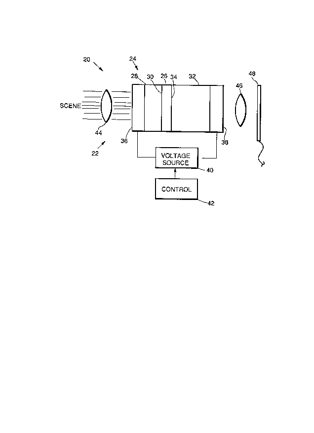
Flgure 1 depicts a sensor system 20 including
a controllable filter 22 accordlng to one embodiment
of the lnventlon. The controllable fllter 22 ls
based upon a quantum well filter unlt 24. Flgure 1,
like the other schematlc deplctions of structure
herein, ls not drawn to scale.
The quantum well fllter unlt 24 lncludes a
quantum well layer 26 made of an lnfrared
transparent semlconductor materlal. A flrst barrler
layer 28, havlng a flrst barrier layer thlckness,
epltaxially contacts a first slde 30 of the quantum
well layer 26. A second barrler layer 32, having a
second barrier layer thlckness, epita~lally contacts
a second side ~4 of the quantum well layer 26,
opposite to the first side 30. In the embodiment of
Figure 1, the second barrier layer thickness ls
greater than the flrst barrler layer thickness. The
first barrier layer 28 is made of a second infrared
transparent semiconductor materlal, and the second
barrier layer 32 is made of a thlrd infrared
transparent semlconductor materlal. In the
preferred practice, the flrst barrler layer 28 and
the second barrier layer 32 are made of the same
semlconductor barrler materlal.
2l5q82~
--7--
The quantum well fllter unlt 24 further
lncludes means for controllably lntroduclng charge
carrlers lnto the quantum well layer 26. In the
embodlment of Flgure 1, thls means for controllably
lntroduclng charge carrlers lncludes a flrst doped
cladding layer 36 ln contact wlth the flrst barrler
layer 28 on lts side remote from the quantum well
layer 26, and a second doped claddlng layer 38 ln
contact with the second barrler layer 32 on lts slde
remote from the quantum well layer 26. A voltage
source 40 ls connected by leads to the claddlng
layeræ 36 and 38, so that a voltage may be applled
between the claddlng layers 36 and 38, and thence
across the first barrler layer 28, the quantum well
26, and the second barrier layer 32. A control 42
is operatlvely connected to the voltage source 40 to
permlt operator or computer control of the voltage
source 40.
The above descrlption of the quantum well
filter unlt 24 began wlth the centermost lager 26,
progressed to the adJacent layers 28 and 32, and
then moved to the outermost layers 36 and 38, for
clarlty ln descrlptlon of the functions of the
layers. The quantum well fllter unlt 24 ls not
fabrlcated ln thls manner beglnning wlth the
centermost layer 26, however. Instead, lt ls
typlcally fabrlcated unldlrectlonally in the
sequence of layers 36, 28, 26, 32, and 38, or the
r?verse order. The fabrlcatlon procedure will be
discussed ln more detall subsequently.
The filter 22 lncludes a means for directing
lnfrared radiation through the first barrler layer
28, the quantum well 26, and the second barrier
layer 32. This means typlcally includes an optlcal
system, here depicted generlcally as lenses 44 and
46, that focuses the infrared energy from a scene
-8- 21 S~82
through the filter 22 and onto a detector of
infrared energy such as a detector 48. The optlcal
system may lnclude more complex elements such as an
attenuator, an ampllfler, mlrrors, other lenses,
etc., as needed for partlcular applicatlons. The
detalls of the deslgn of the optlcal system wlll
depend upon each lndlvldual appllcatlon, and elther
or both of the portlons 44 or 46 can optlonally be
omltted. The detector 48 may be of ang operable
type that ls sensltlve to lnfrared radlatlon, and ls
preferably a focal plane detector array made of
lndlum antlmonlde (InSb) or mercury cadmlum
tellurlde (HgCdTe). Such detectors are well known
ln the art, as ls the design of optical systems for
particular applications.
Flgure 2 deplcts the electronlc structure of
the quantum well fllter unlt 24, ln the absence of a
voltage applled by the voltage source 40. Energy
subbands 50 and 52 are created ln the quantum well
layer 26 accordlng to known quantum mechanlcal slze
effects. When no charge carrlers are present, the
quantum well fllter unlt 24 ls transparent to
infrared radlatlon. No substantlal number of charge
carrlers are present ln the absence of an applled
voltage.
When present, charge carrlers (electrons or
holes) resldlng ln the lower energy level 50 can be
promoted to the hlgher energy level 52 through the
absorptlon of lnfrared llght at an energy equal to
30 th~ energy dlfference between the two subbands. As
lllustrated ln Flgure 3, an approprlate voltage
applied between the cladding layers 36 and 38 causes
charge carrlers to move from the doped cladding
layer 36, through the flrst barrler layer 28, and
lnto the quantum well layer 26. The charge carrlers
are blocked from flow to the second doped claddlng
21S~B2~
layer 38 by the thicker second barrler layer 32.
(The claddlng layer 38 ls provlded as an electrical
contact, and also as a source of charge csrriers for
the next quantum well filter unlt that ma~ be placed
to the right of that shown ln Flgure 1, as wlll be
dlscussed subsequently.)
Wlth an applled ~oltage on the order of about
1 volt, the lower subband 50 ls populated wlth
charge carrlers. These charge carrlers can be
exclted to the upper subband 52 by lnfrared energy
of the approprlate wavelength, resultlng ln
absorptlon of lnfrared energy by the quantum well
fllter unlt 24. Flgure 4 shows the result of
applying a voltage on the infrared transmisslon
through the fllter unlt 24. When no voltage ls
applled, there ls nearly complete transmlsslon at
all relevant wavelengths. When a voltage ls
applied, absorptlon occurs wlthin a band
characterlstlc of the geometry and materlals of
constructlon of the quantum well filter unit 24.
The quantum well fllter unit 24 is preferably
fabricated by molecular beam epitaxial growth of the
layers 36, 28, 26, 32, and 38, in that order or ln
the reverse order. The doped claddlng layers 36 and
38 are typically about 200 Angstroms thick. (When
stacked structures of the type discussed below ln
relation to Figure 6 are prepared, the layers 38 and
36 of ad~acent filter unlts are in contact with each
other, and each of the layers 38 and 36 can
there~ore be about 100 Angstroms thick for a total
thickness of about 200 Angstroms.) The first
barrier layer 28 is typically from about 10
Angstroms to about 50 Angstroms thick. The quantum
well layer 26 is typically from about 20 Angstroms
to about 80 Angstroms thick. The thinner the
quantum well layer wlthin the indlcated range, the
21 S4 82~
--10--
shorter the wavelength of the band of absorption
deplcted in Flgure 4. The second barrier layer 32
is typlcally from about 100 Angstroms to about 300
Angstroms thlck. In all cases of the first
embodlment shown ln Flgure 1, one of the barrier
layers ls thicker than the other.
A number of different materials of
constructlon can be used. For example, ln one
comblnatlon the quantum well layer may be galllum
arsenide, the clsdding layers can be beryllium-doped
gallium arsenide, and the barrler layers can be
aluminum arsenide. In another combinatlon, the
quantum well layer can be gallium antlmonide, the
cladding layers can be tellurium-doped gallium
antimonide, and the barrier layers can be aluminum
antimonide. In another combination, the quantum
well layer can be silicon germanlum, the claddlng
layers can be boron-doped silicon germanium, and the
barrier layers can be silicon or germanlum. In
another comblnation, the quantum well layer can be
gallium indium arsenide, the claddlng layers can be
beryllium-doped indium gallium arsenide, and the
barrier layers can be indlum phosphide. In another
combination, the quantum well layer can be gallium
antimonide, the cladding layers can be silicon-doped
gallium antimonlde, and the barrler layers can be
aluminum antimonide. These combinatlons are
provided as e~amples, and other comblnations are
posæible.
Figure 5 depicts another embodlment of the
lnventlon. A sensor system 60 includes a filter
62. The filter 62 has a quantum well filter unlt
64, which ls composed of a quantum well layer 66 and
two barrier layers 68 and 70, one on each slde of
the quantum well layer 66. In thls embodlment, the
barrler layers 68 and 70 can be of equal thlckness,
~ 21~82~
as they functlon only to create subbands in the
quantum well layer 66, or they may be of unequal
thlckness. An optlcal system, lndicated generically
bg the lenses 72, directs infrared energy from the
scene through the quantum well filter unlt 64 and to
a detector 74. No claddlng layers are needed,
because charge carrlers are supplled to the quantum
well layer 66 by non-electrlcal means to be
descrlbed next.
A laser 76, under command of a control 78,
produces a laser beam that ls dlrected lnto the
quantum well layer 66. The laser beam has a
wavelength that e~cites the productlon of charge
carrlers in the quantum well layer 66, thereb~
lS providing optical activation of the quantum well
fllterlng mechanlsm descrlbed previously, rather
than actlvatlon responslve to an applled electrlcal
potentlal. In one deslgn shown ln Flgure 5, a
partlally sllvered mlrror 80 mlxes the laser beam
into the lnfrared energy of the scene, and dlrects
both the laser beam and the infrared energy of the
scene through the quantum well fllter unlt 64. The
laser beam ls absorbed completely b~ the fllter, and
therefore none of the energy of the laser beam
reaches the detector 74. In one operable approach,
the laser beam has a wavelength of 0.8 mlcrons,
below the desired infrared wavelength range for the
system, but capable of e~citing charge carriers ln
the quantum well layer 66. A typlcal system
incorporatlng an indium antimonlde detector 74, for
example, ls sensltlve to infrared radiation in the
3-5 micron wavelength range.
As shown in Figure 4, even when activated by
an applied voltage, a single quantum well filter
3S unit 24 or 64 achleves only a modest degree of
attenuation in the filtered band of lnterest. The
-- 21~g82~
-12-
effective attenuatlon can be lmpro~ed by utlllzlng a
plurallty of the quantum well fllter unlts together,
as shown ln Flgure 6, to form a fllter 90. ~ere,
the quantum well fllter unlts are shown as the flrst
embodlment 24, but the~ could be the second
embodlment 64 or other posslble embodlments. The
voltage from the voltage source can be applled
across each lndlvldual quantum well fllter unlt 24
ln the manner deplcted ln Flgure 1, or a slngle
voltage can be applled across the entlre group of
quantum well fllter unlts 24 as æhown ln Flgure 6.
The doped cladding la~ers between each palr of
fllter unlts can be fabrlcated as a slngle layer
that provides charge carrlers to the adJacent
quantum well. In thls form of fllter havlng a
plurallty of quantum well fllter unlts, the
attenuatlons wlthln the flltered band are
effectlvely multlpllcatlve. That ls, lf the maxlmum
attenuatlon factor for a slngle quantum well fllter
unlt ls 0.5, then for two quantum well fllter unlts
ln serles the attenuatlon factor ls 0.25, for three
quantum well filter unlts ln serles the attenuation
factor is 0.125, etc.
The fllter 90 of Flgure 6 ls operable to
controllably fllter a slngle selected bandwldth of
lnfrared energy. Other bands can be flltered b~
provldlng a fllter 100, as shown ln Flgure 7. The
fllter 100 ls shown as belng based upon the second
embodlment of Flgure 5, but lt could be based upon
the f~rst embodiment of Flgure 1 or other
embodlments of the quantum well fllter unlt.
The fllter 100 has several, here shown as
three, fllter arra~s 102, 104, and 106 of fl~ed-band
pass quantum well fllter unlts 64. The fllter
arrays 102, 104, and 106 are arranged so that the
lnfrared radlation from the scene passes through all
- 215~82~
-13-
of the fllter arrays. The quantum well fllter unlts
of each of the fllter arrays are comparable ln
construction to those dlscussed ln relatlon to
Flgure 5, but are tallored to be absorbent for
dlfferent bands wlthln the lnfrared spectrum. For
example, the respectlve quantum wells of the quantum
well fllter unlts found ln the fllter arrays 102,
104, and 106 could be made of dlfferent thicknesses
so as to deflne subbands that absorb at dlfferent
wavelengths of lncldent energy. Thus, the filter
array 102 mlght have quantum wells of 80 Angstroms
thickness, the fllter array 104 might have quantum
wells of 70 Angstroms thickness, and the filter
array 106 might have quantum wells of 50 Angstroms
thickness.
Flgure 8 deplcts the attenuatlon of the
fllter 100 of Flgure 7. The bandwldth of the
attenuated band ls broadened because of the multlple
fllter arrays 102, 104, and 106. In thls case, by
vlrtue of the mode of constructlon all of the fllter
arrays are elther on or off. If the electrlcally
controllable approach of the flrst embodiment of
Flgure 1 were used lnstead, the fllter arrays could
be turned on or off in selected comblnations to
block or pass varlous comblnatlons of lnfrared
bands.
If accurate spectral tallorlng ls requlred,
the quantum well fllter(s) can be used in
con~unction with conventional flxed band pass
optical filters that are placed in the optical train
in series with the quantum well filter(s). Such
conventlonal fixed band pass optical fllters and
their fabrication are well known in the art. By way
of e~ample, the spectral response characteristic of
three such fixed filters covering slightly different
band widths, and placed in series, is shown in
21 5~82~
Flgure 9.
Figure 10 deplcts a filter 110 ln whlch three
controllable quantum well fllters 112, 114, and 116
are placed ln serles ln the optlcal traln wlth three
flxed band pass optlcal filters 118, 120, and 122.
The quantum well filters 112, 114 and 116 can be
actlvated b~ elther of the electrlcal or laser
technlques dlscussed prevlousl~. In thls deplcted
embodiment, the quantum well filters are shown as
actlvated bg three lndependent voltage sources 124,
126, and 128. The voltage sources ln turn are
controlled b~ a control 130 that actlvates the
quantum well filters ln some coordinated fashion.
An optical system represented by lenses 132 and 134
is provlded to dlrect the energ~ from the scene
through the filter and onto a device such as a
detector 136.
Figure 11 shows the spectral transmission
functlon that can be obtalned when the controllable
quantum well filters of the inventlon are placed
lnto an optical train ln series with such flxed band
pass optical fllters, as shown ln Figure 10. In
such a devlce, each of the three quantum well
fllters can be controllabl~ turned on or off by the
appllcatlon of a voltage or use of a laser to obtaln
a controllable spectral response that ls
superlmposed upon the spectral response of the flxed
fllters. B~ thls series placement of selected
combinatlons of controllable quantum well filters of
the same or different types, and fixed filters of
the same or dlfferent t~pes, a wlde range of
controllably tallorable spectral responses can be
obtalned ln a slngle fllter unlt posltloned ln the
optlcal traln ahead of the detector or other optlcal
device.
The ablllty to select the bands of infrared
2l~824
energ~ falling on the detector ls a partlcular
advantage of the present lnvention. The most
favored band of energ~ to sense can depend upon the
content of the scene includlng the obJects of
lnterest and clutter, lightlng conditlons,
countermeasures ln a mllltar~ envlronment, the range
of the scene, and other factors. The ablllty to
select the band of lnfrared energ~ reachlng the
detector, rellabl~, qulckl~, and wlthout mechanlcal
devices, greatl~ increases the utlllt~ of the sensor
s~stem.
Although partlcular embodlments of the
lnvention have been descrlbed in detall for purposes
of lllustratlon, varlous modlflcatlons and
enhancements may be made wlthout departlng from the
spirit and scope of the lnventlon. Accordlngl~, the
inventlon ls not to be llmlted except as b~ the
appended claims.