Note: Descriptions are shown in the official language in which they were submitted.
'~ 21~15~
WAITE- 1
RECON~IGURABLE FAULT CON~ROL APPARATUS
~I~;LD OF THE INVENTION
This invention relates generally to fault tolerant process controllers and more
5 particularly to fault tolerant process controllers used to monitor the flow of fluids or gases
throughout a system.
BACKGROUND OF THE INVE~TION
By the turn of the century the field of automatic process control had become an
10 area of concentrated scientific research. The idea of using m~chin~s rather than people to
monitor automatic processes was attractive to busin~ssm~n seeking to stre~mline their operations.
Automatic monitors could operate continuously, at a low cost, and they could be equipped to
rapidly respond to ch~n~ing conditions in the monitored process. These m~chin~s were
"intelligent" in the sense that they employed logical elements to "make decisions" about the state
of the process based on information received through process sensors. After eval~l~ting the
information, an automatic monitor could set the state of the monitored process according to some
preset sequence of instructions. The earliest automatic process controllers were limited to one
preset le;,p..~se. However, as the logical elements of the monitors evolved adaptive responses
became possible.
The logical elements of automatic process controllers evolved steadily from their
modest beginnings to the current state of the art. They progressed from electro-m~rh~ni~al
' 21~51$~
_ ~evices and pnP~Im~tirs, to electron tubes, and eventually, to logic gates composed of multiple
transistors. The advent of transistors quickly led to the use of integrated circuits and, in turn,
to the use of microprocessors. By the late 1960's the col~lpllt~,. was introduced as the main logic
element of automatic process controllers.
The use of microprocessors and computers as the main logic elements of automaticprocess controllers gave designers the freedom to implement complex control processes which
could respond to any number of problems within the monitored process. One problem that
designers set out to solve was that of continuity of the process. This problem arises when a
critical element within the control loop begins to malfunction, giving rise to an error indication
and corresponding process shutdown. Such a shutdown could have disastrous consequences.
For exarnple, the dire results of a failure in a critical el~ e.lt of an aircraft's fuel supply system
which caused the process controller to direct a shutdown of the entire fuel system, without a
backup mode in place, are obvious. To solve continuity of process problems such as this,
designers made use of micropIocessor controlled logic elements to implement "fail safe" designs
lS that would avoid process shutdowns.
Automatic process controllers began to incorporate systems that would m~int~in
the process in a static condition upon the occwlence of a failure. An example of such a fail safe
design is the crash avoidance m~ch~ni~m present in many of today's jet fighter planes. The
planes are equipped with sensors capable of detecting the pilot's loss of consciousness or
"blackout" - an event which may occur when the pilot is execl~ting high g force maneuvers. In
the event that a "blackout" is detected the plane's control surfaces are adjusted via computer to
m~int~in straight and level flight. ~n this manner, a blackout will not result in the loss of the
215Sl~
plane and pilot. While fault tolerant systems which can m~int~in processes in a static condition
offer many advantages, even greater advantages are realizable by systems that capable of
implementing one of several static conditions.
Fault response systems which m~int~in a process in a static condition are usually
hardwired. This makes them difficult to reconfigure without burdensome re-wiring. Thus, they
are inflexible and can not be adapted to ch~nging conditions in the monitored process.
In overcoming the disadvantages of prior-art process controllers, the present
invention provides easily reconfigurable fault re~ponse circuitry. The invention allows the fault
response of the system to be varied either by a human operator or through additional logical
10 elements, thereby providing a highly flexible fault response.
SUM~IARY OF THE INVENTION
It is an object of the present invention to provide fault control circuitry for
automatic process controllers and to provide means for easily reconfiguring the circuitry to
15 change the fault response.
That object is achieved through the use of a plurality of control relays that are
responsive to a fault detection circuit. When a fault is ~etected the circuit selectively opens or
closes the relays for the duration of the fault. Accordingly, the process elements that are
controlled by the relays will be selectively turned on or off for the duration of the fault. The
20 fault lesponsi~e state of each relay, and hence the state of the elem~ntc they control, is
determined by a matrix of switched connections which provide great flexibility in the fault states
Ihat may be implemented.
:' 2~ 15~
In addition to providing switching for various process ele.llea~, the fault control
circuitry may be used to generate a control signal in the event that the controller can no longer
genelate such a signal. A "fail safe" control signal is turned on by one of the relays in response
to a failure indication from the fault detection circuit. The control signal may be a digital or an
5 analog signal, and in a ~lefel~d embodiment is an analog signal. The level of the analog
control signal is preset and may be varied within a built in range of values through the use of
any of various well-known means for varying a voltage or current output.
It is a further object of the present invention to provide a cost effective means of
protecting the analog input circuitry of an automatic process controller.
The desired protection of the analog input components is achieved by inserting
a resistor between the analog input terminals of an automatic process controller. In the event
that the analog signals received from the process sensors are ill~e.r, ~d with, causing a fault such
as an incorrect polarity, a short circuit, or a higher than normal pot~ntial, the resistor will
receive the full impact of the fault and acts as a fuse. The resistor provides protection for the
15 analog circuitry, it is cheap, and it is easily replaceable. In the event a fault does occur and the
resistor is sacrificed, a technician needs only to unplug the "burnt" resistor and plug in a new
one.
In an illll5tT~tive embodiment the fault response circuitry of the present invention
is used in a fluid control system. Relays are used to turn on variable speed pumps while the
20 analog control signal is used to set the speed of the pumps. Each analog input terrninal has two
jumper sockets into which a protective resistor is inserted.
According to a first broad aspect, the present
invention provides a fault control circuit for use with an
automatic process controller generating at least one relay
signal, comprising: a fault detection circuit for sensing an
interruption of a clock signal and providing a fault
indication signal and a relay disabling signal upon
interruption of said clock signal; at least one first
electrically-triggered switching means operative to control
the automatic process in response to said at least one relay
signal, said first switching means being switched to a
predetermined fault position in response to said fault
indication signal and said relay disabling signal; a switching
circuit; and selection means which, together with said
switching circuit, selectively determine said predetermined
fault position of said first switching means, wherein said
relay disabling signal disables said at least one relay signal
and, said fault indication signal enabling the settings of
both said switching circuit and said selection means to
establish said predetermined fault position of said first
switching means.
According to a second broad aspect, the present
invention provides a microprocessor-based fault control
circuit for use in a flow control system, comprising: a fault
detection circuit for sensing an interruption of a
microprocessor clock signal, said fault detection circuit
provides a fault indication signal upon interruption of said
microprocessor clock signal; at least one first relay
operative to control at least a portion of said flow control
- 4a -
72432-92
.ç~'~
7 ~ a ~, ~ ~ ~
-- :.
.",.~,.
system, said at least one relay being set to a predetermined
fault position in response to said fault indication signal; a
switching circuit; and selection means which, together with
said switching circuit, selectively determine said
predetermined fault position of said first relay, settings of
said switching circuit and said selection means being used to
preset said determination fault position of said first relay.
According to a third broad aspect, the present
invention provides in a fluid flow controller of the type
employing a microprocessor to control electrically powered
pumps that drive the flow of fluid throughout a predefined
environment, each pump being operable from a high level power
supply and a low level power supply, and at least one of said
pumps having an output speed variable in proportion to an
input signal, a microprocessor-based fault control circuit,
comprising: a fault detection circuit for sensing an
interruption of a microprocessor clock signal, whereby, said
fault detection circuit provides a fault indication signal
upon interruption of said microprocessor clock signal; a
plurality of relays operative to control said pumps, at least
one first relay being disposed for coupling a high level power
supply to at least one pump, and at least one second relay
being disposed for coupling a low level power supply to at
least one pump, whereby said plurality of relays are each set
to a predetermined fault position in response to said fault
indication signal; a switching circuit; a selection means
which together with said switching circuit, selectively
determine said predetermined fault positions of said plurality
- 4b -
72432-92
~!,'.~
f~
of relays, the settings of said switching circuit and said
selection means being used to preset said predetermined fault
positions of said plurality of relays; a fault-activated
output circuit operative to provide a signal used to set the
speed of said pumps having an output speed responsive to an
input signal; and a means responsive to said fault indication
signal for activating said fault-activated output circuit.
- 4c -
72432-92
' 215~15~
~- BRlEF DESCRIPIION OF THE DR~WINGS
FIG. 1 is a block diagram of the apparatus of the invention.
FIG. 2 is a sch.~ diagram of an illustrative embodiment of the invention.
FIG. 3 is a block diagram of the invention including an analog output portion.
FIG. 4 is a schematic diagram of an illustrative embodiment of the invention
including an analog output portion.
FIG. S is a sch~ ic diagram of the analog input portion of an automatic process
controller having analog input fault protection as set forth in the present invention.
2i~515~
DETAILED DESCRIPI ION
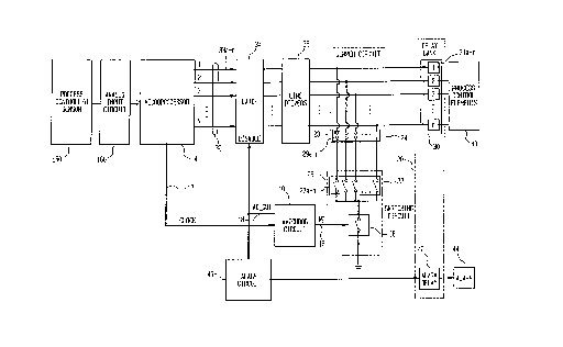
Refe~ling now to FIG. 1, there is shown a block diagram of an automatic process
controller employing the present invention. As can be seen from the diagram, the controller may
effectuate cor.trol over the process by means of one or more relays 30 that are used for the
5 switching of one or more process control elements 40. When the controller is functioning
correctly the positions of the relays 30 are determined by one or more relay signals 32 generated
by a microprocessor 14. However, in the event that the microprocessor should fail or be
removed the position of the relays will be deterrnined by a jumper circuit 24 and a switching
circuit 22. Thus, it is the jumper circuit 24 and switching circuit 22 that determine the fault
~0 response state of the process control elements 40 by setting the fault positions of the relays 30.
The fault respoDse of the controller is triggered by means of a watchdog circuit
10. The watchdog circuit 10 continuously monitors a clock signal 12 generated by the
microprocessor 14. If the microprocessor 14 fails or is removed the rec~lting absence of the
clock signal 12 will actuate the watchdog circuit 10. When activated, the watchdog circuit
15 gen~r~tes two signals, an AC-OUT signal 18 that disables the relay signals 32, and a watchdog
signal 18 that enables the jumper circuit 24 and switching circuit 22. In this manner the fault
response, as determined by the jumper circuit 24 and switching circuit 22, is triggered by the
watchdog circuit 10.
In order to more fully appreciate the operation of the present invention a detailed
description of the circuitry associated with an single relay 31a will be provided. It will be
understood that one of ordinary skill in the art of circuit design can duplicate the circuitry
21~5159
associated with relay 31a to provide for the simultaneous control of any desired number of relays
- as illustrated in the diagram by the circuitry associated with relays 31b-n.
Refe~ g further to FIG. 1, it can be seen that under normal opelaling conditionsa relay signal 33a generated by the microprocessor 14 is passed to a line driver 36 by means of
a latch 34. The latch 34 ensures the stability of the relay signal 33a, while the line driver 36
amplifies the output of the latch 34 so that the propagation losses do not degrade the sianal tO
the point where it would not be effective for setting the position of the relay 31a. The line driver
36 is coupled to the input of the relay 31a and serves to isolate the output of the latch 34 from
the input of the relay 31a. The jumper circuit 24 is also coupled to the output of the line driver
36, with the s~vilching circuit 22 being coupled to the jumper circuit 24 and providing a path
from the output of the line driver 36 to ground. When a jurnper is inserted into jumper contact
29a and switch 27a is closed, an absent microprocessor clock signal 12 will result in the
grounding of the input to relay 31a. This grounding occurs because the watchdog signal 16,
generated in response to the missing clock signal activates the switching circuit 22 by closing
a switching circuit enabling switch 38, thereby completing the path from the input of relay 31a
to ground. Once the input of relay 31a is grounded, relay 31a will revert to its "grounded" or
"fault" position, regardless of the value of the output of the line driver 36.
The output of relay 31a is used to control some aspect of the controlled processthrough one or more process control elements 40. The fault position of the relay 31a - as
predetermined by the plesence or absence of a jumper at contacts 29a and the position of switch
27a - will therefore determine the state of one or more process control elements upon the
occurrence of a fault. As can be seen from FIG. 1. any number of relay input lines 32 may be
' 215515~
imple.lle,lted. ~f n lines 32 are irnplemented, then n contacts 28 and n switches 26 will be
required to illdepel~dently control the fault response of each of n relays 30. Of course, one of
the contacts 28 may be coupled to more than one relay 30 so that n relays 30 may be controlled
by less than n contacts 28. Similarly, one of the switches 26 may be used to switch more than
S one relay 30.
Referring further to FIG. 1, it can be seen that an additional relay 42 is used to
trigger an alarm 44. Relay 42 is controlled by an alarm circuit 46 that is, in turn, controlled by
the watchdog circuit 10. In the event of a fault, the AC-OUT signal 18 generated by the
watchdog circuit disables the latch 34 and enables the alarm circuit 46. The alarm circuit then
triggers the alarm 44 through the alarm relay 42.
In addition to providing relay fault positions and the triggering of an alarm relay,
the invention provides a fault ~ ~nse for those process control elçm~n~ that require analog
inputs.
Refe.ling to FIG. 3, there is shown a block diagram of an automatic process
controller having process control elements 340 requiring analog inputs and employing the present
invention. A microl~r~cessor 314 generates outputs 332 which may be used to control relays 30
as well as to set the level of the analog inputs required by the process control elements 340.
When used to set the level of the analog inputs, the microprocessor outputs 332 are coupled to
a Digital to Analog (D/A) converter 370. The output of the D/A converter 370 is coupled to an
analog signal conditioning circuit 372 which conditions the signal so that it is in a forrn that is
usable by the process control elements 340. Under normal operating conditions, the output of
215~159
~_,he analog signal conditioning circuit 372 is coupled to the process control elements 340.
However, in the event that the micropr~cessor 314 fails or is removed, the output of an analog
signal ge~ dtol 374 is sub~ d for the output of the analog signal conditioning circuit 372.
This substitution is achieved by means of a switch 376 that is responsive to a WD-DRV signal
generated by a switching circuit 322. The operation of the switching circuit 322 is the same as
the operation of the switching circuit 22 shown in FIG. 1. When a watchdog circuit 310 detects
a fault, it activates the switching circuit 322 through an enabling switch 338. In the configuration
of FIG. 1, the enabling switch 38 merely activates the switching circuit 22. In the configuration
of FIG. 3, the enabling switch 338 not omy activates the switching circuit 322 but it also throws
switch 376 so that the output of the analog signal generator 374 is substituted for the output of
the analog signal conditioning circuit 372. In t'nis manner an analog fault response is provided.
An illustrative embodiment of the above described invention is illustrated in
figures 2, 4, and 5. The illustrative embodirnent shows the invention as it is applied in a fluid
control system. The system has two pumps that control the flow of a fluid throughout a building,
each pump requiring a high output power supply and a low output power supply. Four relays
are required to switch the power supplies corresponding to each pump. Accordingly, FIG. 2
shows a relay bank 230 c~ln~ g eight relays 231a-h, four for each pump. The relays 230 are
opened and closed in response to relay signals 232 generated by a microprocessor 214. The
circuitry of the illustrative embodimen~ includes: a latch 234. line drivers 236a and 236b, a
jumper circuit 224, and a ~vi~hing circuit 222, all of which function similarly to their analogous
circuit elements in FIG. 1. Like the circuitrv associated with each relay 31a-n of FIG. 1, the
2~sl59
_ circuitry associated with each relay 231a-h is the same, thus a detailed description of the
circuitry associated with a single relay 231a will be provided with the underst~n-ling that
circuitry associated with relays 231b-h operates in the same fashion.
Under normal operating conditions, the microprocessor 214 will control the
5position of relay 231a through a relay signal 233a. The signal 233a is passed through a latch
234a to a line driver 237a, the latch 234a being responsi-e to a clock signal 217 A resistor 48a
of a resistor network 48a-h couples the input of the line driver 237a to ground. The line driver
237a provides amplification and buffering of the output of the latch 234a. The output of the line
driver 237a is coupled to relay 231a by means of the jumper circuit 224. The relay 231a will
10be responsive to the output of the line driver 237a unless a fault is ~etected, in which case the
relay will be responsive to the jumper circuit 224 and switching circuit 222a.
A jumper inserted into a contact 50a of contact network 50a-h, or a jumper
ed into contact 52a of contact l~elw~l~ S2a-h, of the jumper circuit 224 will provide a path
from the input of relay 231a to ground when a fault condition exists. The pl~sel~ce of a jumper
15between contacts 50a couples the relay 231a to a switch 54 of the switching circuit 222 - diodes
60a and 62a of diode networks 60a-h and 62a-h, ensuring a uni-directional flow of current from
the input of relay 231a to ground. The switch 54 is coupled to a MOSFET 58 that is activated
by a watchdog signal 216 generated by a watchdog circuit 210. When there is a jumper inserted
in contacts 50a, switch 54 is closed, and the watchdog signal 216 is high, the input of relay 231a
20will be coupled to ground. Alternatively, but in a similar manner, a jumper inserted in contacts
52a, a closed switch 56, and a high watchdog signal 216 will also couple the input of relay 231a
to ground. When either of the conditions for the grounding of the input of relay 231a is met.
~S159
the relay 231a will be set to its fault position. By selectively inserting jumpers into contacts 50a-
h and 52a-h and by presetting switches 54 and 56 the fault positions of relays 231a-h, and thus
the fault response of each pump, may be reconfigured at any time.
Referring further to FIG. 2, an illustrative embodiment of a watchdog circuit 210
is shown. The watchdog circuit 210 continuously monitors a clock signal 212 from the
microprocessor 214 and generates a watchdog signal when an interruption of the clock signal
212 is detected. The clock signal 212 is used as input to both terminals of an OR gate 264, the
output of the OR gate 264 being coupled to the anode of a diode 266 and a first terminal of a
capacitor 268. The cathode of the diode 266 and a second terminal of the capacitor 268 are
coupled to the base terminal of a PNP transistor t70. Also coupled to the transistor 270 are: a
resistor 272, coupling the base to ground; a resistor, 274 coupling the emitter to a dc power
source 275; a diode 278, with its anode connected to the emitter and its cathode connected to
the dc power supply 275; a capacitor 276, coupling the emitter to ground; and a first input
terminal 280a of an OR gate 280. The capacitor is charged through resistor 274 by the dc power
lS source 275 when transistor 270 is in an "off" state. However, the pulses of the clock signal 212
periodically provide a high voltage level that turns transistor 270 "on", allowing capacitor 276
to discharge. In this manner the voltage at a first input terminal 280a of the OR gate 280 is
m~int~in~d at a low level. As long as the voltage level at a second terminal 280b of OR gate 280
remains low, the watchdog signal 216 will remain low and the fault re~l)onse of the system will
not be triggered.
The fault response of the system may be triggered m~nl~lly by means of a timeoutswitch 288 that is coupled to the second terminal 280b of the OR gate 280. When the switch 288
2 1~5~9
is open the second terminal 280b is coupled to ground through a resistor 290, when the switch
." _
is closed the terminal 280b is coupled to a high voltage level. A high voltage level at the
terminal 280b drives the watchdog signal 216 high, regardless of the value at the first ~rmin~l
280a, thereby forcing activation of the system fault response. One advantage of the timeout
S switch 288 is in providing a means to test the fault response of the system after each
reconflguration .
The watchdog circuit 210 further provides an AC-OUT signal 218 and a visual
alert, in the forrn of a red light 285, indicating that a fault has occurred. An OR gate 282 having
the watchdog signal 216 as input to both its terrninals, provides a high output when the watchdog
signal 216 goes high. The output of the OR gate 282 is coupled tO the anode of the red light 285
through a resistor 284. When the output of the OR gate 282 is driven high the light 285 turns
on to alert the system operator that a fault has occurred.
The AC-OUT signal 218 is the output of an OR gate 286 having input tem~inals
286a and 286b. The input to terminal 286b is the watchdog signal 216. Terminal 286a is
coupled to a first terminal 291 of a resistor 290 and to ground through a capacitor 292. A second
terminal 293 of the resistor 290 is coupled to an OUTEN signal 287 and to a first terrninal 295
of a resistor 288. A second terminal 297 of the resistor 288 is coupled to a power source 299
that supplies a high logic level voltage to the second tenninal 297. The capacitor 292 is charged
by the power source 299 when the OUTEN signal 287 is high, re~lti~ in a high voltage at
terminal 286a. When the OUTEN signal 287 is low, the capacitor will discharge an a low
voltage will be present at terminal 286a. In this configuration either a high value of the
watchdog si2nal 216 or a high value of the OUTEN sianal 287 will drive the output of the OR
12 i
2155-3 5~
_ gate 286 high and will result in a high value of the AC-OUT signal 218. The AC-OUT signal
has two functions, when driven high it disables the latch 234 and triggers the alarm circuit 246.
The alarm circuit 246 functions to set an alarm relay 242 in the event of a fault.
The alarm circuit comprises: a latch 294, a resistor 296, a MOSFET 2100, and a diode 298.
Relay signal 233h is input tO pin SD of the latch 294. The signal is clocked through the latch
by a clock signal 219 and is output at pin SQ. In the event of a fault the latch 294 is disabled
by the AC-OUT signal 218, thereby swiLching the gate voltage of the MOSFET 2100 and setting
the fault position of the alarm relay 242. The gate of the MOSFET 2100 is coupled to ground
by resistor 296 and the drain of the MOSFET 2100 is coupled to the anode of diode 298. The
cathode of diode 298 is couple to one of the input terrninals of the relay 242 while the anode is
coupled to the second input t~min~l of the relay 242. The alarm relay 242 may be used to
switch on an alarm that will alert a remote system operator that a fault has occurred.
The watchdog circuit 210 of the illustrative embodiment depicted in FIG. 2 not
only triggers the fault response of the relays 230 and alarm relay 242, it also triggers an analog
portion of the fault rc~ponse. The analog portion of the fault response circuitry is shown in FIG.
4. It includes: a D/A convener 470, an analog signal conditioning circuit 472, an analog signal
generator 474, and a switch 476. Each of these elc,llcn~ ~lrOl.l, the same function as their
analogous el~ x depicted in FIG. 3. When operating normally, a microprocessor 414
generates the desired analog signal level - in a digital form - over digital lines 432 to the D/A
converter 470. The D/A converter 470, driven by a clock signal 4101, converts the digital
information to an analog signal that is input to the analog conditioning circuit 472. The analog
signal conditioning circuit 472 funher conditions the signal prior to use by one or more process
~i5~15~
_ control elements 440 which re~uire analog inputs. However, in the event of a fault, the switch
476 decouples the output of the analog conditioning circuit 472 from the process control
elements 440 and couples the output of the analog signal generator 474 to the process control
elements 440. A capacitor 4144, coupling the output of the switch 476 to ground helps protect
S the analog signal from AC corruption.
As can be seen from FIG. 4, the analog signal conditioning circuit 472 is
comprised of: resistors 4102, 4104, 4106, 4108, 4112, 4114, 4116, 4120, and 4122; a
comparator 4110: an NPN transistor 4118: and jumper contacts 4124a, 4124b, and 4124c. The
aforementioned elements being coupled together as shown in FIG. 4. The jumper contacts
10 4124a-c are used to determine the form of the analog signal that will be input to the process
control elements 440 during normal operation. When a jumper is inserted between contacts
4124a and 4124b a 0 - 20mA signal will be input to the control elem~t~ 440, when a jumper
is inserted between contacts 4124b and 4124c a 1 - lOV signal will be input to the elements 440.
In either case, the switch 476 will decouple the analog signal conditioning circuit 472 from the
15 process control elements 440 when a fault occurs.
Referring further to FIG. 4, the switch 476 is co.,lylised of a relay 479 and a
diode 4126 with its cathode coupled to a first terminal 479a of the relay and its anode coupled
to a second te~min~l 479b of the relay 479. Another input to the second terminal 479b of the
relay 479 is a WD-DRV signal 478. The WD-DRV signal goes low when a fault occurs, thereby
20 causing the relay 479 to switch to its fault position in which the output of the analog signal
generator 474 is coupled to the process control elements 440.
- ~15~15~
The analog signal generator 474 is co--lplised of: resistors 4128, 4134, 4138, and
4142; a capacitor 4132; an NPN transistor 4136; a potentiometer 4130; and jumper contacts
4140 - these cl~ s being coupled together as shown in FIG. 4. The potentiometer 4130 is
used to set the value of the analog signal that is output from the analog signal generator 474
S while the form of the signal - either a constant voltage or current - is set by the absence or
presence of a jumper at jumper contacts 4140. Through the use of the potentiometer 4130 and
the jumper contacts 414 an easily reconfigurable analog fault response is realized.
~n addition to providing a relay fault response and an analog fault response, the
10 present invention provides for the protection of the automatic process controller from potentially
destructive inl~re~ce in the analog signals that are received from the process sensors.
R~f~ ~g now to FIG. 5, there is shown an illustrative embodiment including
eight process control sensors 5150a-h, an analog input circuit 5160, and a microprocessor 514.
15 These three elements correlate, .e~ ely, to process controller sensors 150, analog input
circuit 160, and microprocessor 14 of FIG. 1. The process control sensors 5150a-h moni~or
various palallleters associated with the process, and relay that il~o~ ion to the controller's
microprocessor 514 where it is used to help deterrnine the app~pliate control settings. Since
the circuitry associate~ with each one of the eight process control sensors 5150a-h is the same,
20 a detailed description of the circuitry associated with one process control sensor 5150a will be
sufficient to provide an underst~n~ing of the operation of the illustrative embodiment.
2 1 ~
As shown in FIG. S, process control sensor 5150a is coupled to a pair of jumper
contacts 5162a and 5163a. The contacts 5162a and S163a are coupled to each other through a
prutec~ive resistor 5164a. Contact 5162a is coupled to a first t~rnin~l 5173a of a comparator
5174a through a resistor 5166a, and contact 5163a is coupled to a second terminal 5175a of the
S comparator 5174a through a resistor 5168a. The contact 5163a is also coupled to ground through
a fuse 5186. The first terminal 5173a of the comparator 5174a, a resistor ~170, and the fuse
5186 are coupled together in series to form a path from the terminal 5173 to ground. The second
terminal of the comparator 5175a is also coupled to the output of the comparator 5180a.
Under normal ope-dling conditions the comparator 5174a arnplifies and buffers
the output of the process sensor 5150a to generate an output signal 5180a that is input to a
multiplexer 5182. The multiplexer 5182 filn~tion~ to seq~len~i~lly couple lhe output of each
comparator 5174a-h to an analog to digital converter 5184, which, in turn, converts the output
of the multiplexer 5182 to a digital form that can be "read" by the microprocessor 514. In this
manner, the data from the process sensors 5150a-h can be monitored by the automatic process
controller's microprocessor 514.
The principal advantage of the configuration of FIG. 5 is realized by the provision
of the protective resistors 5164a-h and the contacts 5162a-h and 5163a-h. The protective
resistors 5164a-h function as conversion resistors while plo~ec~ g the co~ponent~ of the analog
input circuit 5160 from potentially destructive faults. The resistors 5164a-h. which may be of
the metal film type, act as fuses which are sacrificed in the event of such a fault. For example,
if the output of the process sensor 5150a were to be accidently coupled to a higher than normal
16
~55~5~
potential, the protective resistor 5164a would be sacrificed, thereby protecting the other
components of the analog input circuit 5160 from damage.
Repl~~em~nt of such a blown resistor is f~~~ ted by the contacts 5162a and 5163a which al~ow
a technician to simply unplug the burnt resistor and plug in a new one. Further protection against
5 high level i ltelr~.ence is provided by the fuse 5186 which is in cornmon with all the contacts
5163a-h.
Herein, a circuit for providing microprocessor fault control has been described.
Although the present embodimeM of the invention has been described in detail it should be
10 understood that various changes, alteratiorls~ and substitutions can be made therein without
d~palli~g from tbe spirit of the inven~ion.