Language selection

Search

Patent 2156323 Summary

Third-party information liability

Some of the information on this Web page has been provided by external sources. The Government of Canada is not responsible for the accuracy, reliability or currency of the information supplied by external sources. Users wishing to rely upon this information should consult directly with the source of the information. Content provided by external sources is not subject to official languages, privacy and accessibility requirements.

Claims and Abstract availability

Any discrepancies in the text and image of the Claims and Abstract are due to differing posting times. Text of the Claims and Abstract are posted:

  • At the time the application is open to public inspection;
  • At the time of issue of the patent (grant).
(12) Patent: (11) CA 2156323
(54) English Title: INLINE ELECTRON GUN HAVING IMPROVED BEAM FORMING REGION
(54) French Title: CANON ELECTRONIQUE DE TYPE IN-LINE A REGION DE MISE EN FORME DE FAISCEAUX AMELIOREE
Status: Expired and beyond the Period of Reversal
Bibliographic Data
(51) International Patent Classification (IPC):
  • H01J 29/48 (2006.01)
(72) Inventors :
  • PONTAILLIER, YVES (France)
  • LAUZIER, RODOLPHE (France)
(73) Owners :
  • THOMSON TUBES AND DISPLAYS, S.A.
(71) Applicants :
  • THOMSON TUBES AND DISPLAYS, S.A. (France)
(74) Agent: CRAIG WILSON AND COMPANY
(74) Associate agent:
(45) Issued: 2000-01-25
(22) Filed Date: 1995-08-17
(41) Open to Public Inspection: 1996-02-27
Examination requested: 1995-08-17
Availability of licence: N/A
Dedicated to the Public: N/A
(25) Language of filing: English

Patent Cooperation Treaty (PCT): No

(30) Application Priority Data:
Application No. Country/Territory Date
94 10312 (France) 1994-08-26

Abstracts

English Abstract


An improved inline electron gun includes a plurality of
electrodes spaced from three cathodes in the direction of a
longitudinal axis of the gun. The electrodes form at least a beam
forming region and a main focus lens in the paths of three
electron beams, a center beam and two side beams. Each of the
electrodes includes three inline apertures therein for passage of
the three electron beams. The beam forming region includes the
cathodes and three consecutive electrodes, a G1 electrode, a G2
electrode and a G3 electrode. The improvement comprises the G2
electrode having two linear projections on either side of the inline
apertures therein. The projections parallel the inline direction of
the apertures protrude in a direction parallel to the longitudinal
axis, past the apertured portion of the G3 electrode in overlapping
relationship therewith. On the side of the G3 electrode facing the
G2 electrode, the G3 electrode has two linear channels therein on
either side of the inline apertures therein. The channels are
immediately adjacent the projections on the G2 electrode and in a
spaced nested relationship therewith.


Claims

Note: Claims are shown in the official language in which they were submitted.

5
CLAIMS
1. In an inline electron gun, including a plurality of
electrodes spaced from three cathodes in a direction of a
longitudinal axis of said gun, said electrodes forming at least a
beam forming region and a main focus lens in the paths of three
electron beams, a center beam and two side beams, each of said
electrodes including three inline apertures therein for passage of
said three electron beams. and said beam forming region including
said cathodes and three consecutive electrodes, a G1 electrode, a
G2 electrode and a G3 electrode, the improvement comprising
said G2 electrode having two linear projections therein on
either side of the inline apertures therein, said projections
paralleling the inline direction of said apertures and protruding in
a direction parallel to said longitudinal axis past an apertured
portion of said G3 electrode in overlapping relationship therewith,
and
on the side of said G3 electrode facing said G2 electrode, said
G3 electrode having two linear channels therein on either side of
the inline apertures therein, said channels being immediately
adjacent said projections on said G2 electrode and in a spaced
nested relationship therewith.
2. The inline electron gun as defined in Claim 1, including
the distance between each one of said projections of said G2
electrode to the immediately adjacent one of said channels of said
G3 electrode being approximately 30% to 50% greater than the
distance between said G2 electrode and said G3 electrode at the
respective apertured portions thereof containing respective ones
of said inline apertures.

Description

Note: Descriptions are shown in the official language in which they were submitted.


2I 56323
RCA 87,244
INLINE F.T T~.CTRON GUN HAVING IMPROVED
BEAM FORMlNG REGION
The present invention relates to inline electron guns, such as
used in color picture tubes, and particularly to such guns having
5 improved structures in their beam forming regions.
An inline electron gun is one designed to generate or initiate
preferably three electron beams in a common plane and to direct
those beams along cv.v~lb~,a~ paths to a point or small area of
Cv~ e near the tube screen. Inline electron guns all have a
10 beam forming region and a main focus lens and may also include a
prefocus lens. The beam forming region usually comprises the
cathodes and three co~ , clc~ udcs. A prefocus lens may
comprise two or three cle~ ud~i,. The main focusing lens is
usually formed by two spaced electrodes.
Usually, the second electrode from the cathodes, called the
G2 electrode, is plate-shaped. Such plate shape makes the G2
electrode subject to bending and flexing during electron gun
operation. It is known to put small beads in the G2 electrodes to
reinforce them. However, even with such reinful~ t, these G2
20 clc.,lludcs still exhibit some flexing during gun operation.
Another problem that occurs in electron guns is arcing
which may occur between the second and third electrodes from
the cathodes (the G2 and G3 clc~lludcs). Such arcing is enhanced
when one of the electrodes has a protrusion on it that faces the
2 5 other electrode.
The present invention addresses these problems by
providing an improved c, u~lion for the beam forming region
in an inline electron gun.
An improved inline electron gun according to the invention
30 includes a plurality of clc,,lludcs~ spaced from three cathodes, in a
direction of a l~n~itll~inql axis of the gun. The el~.,lludc~ form at
least a beam forming region and a main focus lens in the paths of
three electron beams, a center beam and two side beams. Each of
the electrodes includes three inline apertures therein for passage
35 of the three electron beams. The beam forming region includes the
cathodes and three Culls~,ulivt; electrodes, a Gl electrode, a G2

, ,, 21~323
2 RCA 87~244
electrode and a G3 electrode. The il~llJlUV~ cu.ll~,lises the G2
electrode having two linear projections on either side of the inline
apertures therein and parallel to the inline direction of the
apertures. The projections protrude in a direction parallel to the
5 1,; l~itu~iir~al axis, past the apertured portion of the G3 electrode in
overlapping relationship therewith. On the side of the G3
electrode facing the G2 electrode, the G3 electrode has two linear
channels therein on either side of the inline apertures therein.
The channels are j"""r.li;"~ly adjacent the projections on the G20 electrode and in a spaced nested relationship therewith. This
provides a stiffer G2 electrode, and, by modifying
the G3 electrode, it ~ ;, s a possible cause of arcing that may
be created by the i...~,. o v ~ t in the G2 electrode.
In the drawings:
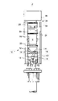
FIGURE 1 is a side view of an electron gun i-.c~.~u.~i.. g an
embodiment of the present invention.
FIGURE 2 is a cross-sectional side view of a prior art G2
electrode and a facing portion of a prior art G3 electrode.
FIGURE 3 is a cross-sectional side view of the novel G2
20 electrode and facing portion of the novel G3 electrode of
FIGURE 1.
In detail, an electron gun 10, shown in FIGURE 1, cu...~,.ises
two insulative support rods 12 on which various electrodes are
mounted. These electrodes include three spaced coplanar
25 cathodes 14 (one shown), a control grid electrode 16 (G1), a screen
grid electrode 18 (G2), a first prefocus electrode 20 (G3), a second
prefocus electrode 22 (G4), a combined third prefocus electrode
and first main focus electrode 24 (G5) and a second main focus
electrode 26 (G6), spaced along the support rods 12 in the order
3 0 named and in the direction of a 1~ I axis Z. Each of the G1
through G6 electrodes has three inline apertures therein, or at
each end thereof, to permit passage of three coplanar electron
beams. The main el~ u~lalic focusing lens in the gun 10 is
formed between the G5 electrode 24 and the G6 electrode 26. The
35 G5 electrode 24 also may be referred to as the focus electrode,
because a focus voltage is applied to it, and the G6 electrode 26

-
21~632~
.
3 RCA 87,244
may be referred to as the anode electrode, because an anode
voltage is applied to it. The G5 electrode 24 is formed from two
cup-shaped elements, 28 and 30, that are c~ at their open
ends. The G6 electrode 26 is formed from two cup-shaped
5 elements, 32 and 34, that also are ~ at their open ends. A
shield cup 36 is attached to the element 34 at the exit of the
electron gun.
All of the electrodes of the electron gun 10 are either
directly or indirectly attached to the two insulative support rods
10 12. The rods may extend to and support the Gl electrode 16 and
the G2 electrode 18, or these two ele~llodf~s may be attached to
the G3 electrode 20 by some other insulative means. Preferably,
the support rods are of glass which has been heated and pressed
onto claws extending from the electrodes, to embed the claws in
1 5 the rods.
The G3 electrode 20 is c , ~' from two cup-shaped
parts that are attached at their open ends. One part forms a
portion of the beam forming region of the gun, and the other part
forms part of the prefocus lens of the gun.
FIGURE 2 shows a prior art G2 electrode 38 and a facing side
of a prior art G3 electrode 40. The closest spacing between these
clu,lludlc~ is between the apertured portion 42 of the G2 electrode
38 and the apertured portion 44 of the G3 electrode 40. Outward
from the apertured portions, an ;~lt..~ r. portion 46 of the G2
25 electrode 38 is spaced from an inf--rm~ f-~ portion 48 of the G3
electrode 40 a distance only slightly greater than the closest
spacing between these electrodes. For example, in one prior art
embodiment, the closest spacing at the apertured portions is 0.76
mm, the spacing between the nearest surfaces of the int~rm~ fe
3 0 portions is 0.89 mm, and the spacing between a point 50 on the
intermediate portion 46 to the G3 electrode 40 is 1.08 mm.
F~GURE 3 shows the G2 electrode 18 and a facing side 52 of
the G3 electrode 20, cur.i,llu~ ,d in accul,' --e with the present
invention. The G2 electrode 18 includes an apertured portion 54,
3 5 having three inline apertures 56 (one shown), and two linear
projections 58 therein on either side of the inline apertures 56.

2 ~ 56323
4 RCA 87,244
The projections 58 parallel each other and the inline direction of
the inline apertures 56. Both of the projections 58 protrude in a
direction parallel to the 1~ ~it~ ~inql axis Z of the electron gun 10
past an apertured portion 60 of the G3 electrode 20, thereby
S somewhat o~ ui--g the G3 electrode 20 in the 1. ~ axis
Z direction. The inclusion of the two linear projections 58 on the
G2 electrode 18 greatly improves the stiffness of the electrode.
However, because of the addition of the two large linear
lulù; ::f`nC on the G2 electrode 18, there is an increased
10 possibility of the projections forming arcing sights if no further
changes are made. To reduce this risk of arcing between the G2
electrode and the G3 electrode, the spacings between the
projections and all points on the G3 electrode are increased by
re~L-ci~r;n~ the shape of the G3 electrode.
15 The G3 electrode 20 includes an intermediate portion 62
that is inclined at a greater angle with respect to the apertured
portion 60 than is the prior art i.-~- ,. r.~ portion 48 with
respect to the apertured portion 44, and that is curved to form
two linear channels 64 therein on either side of the inline
20 apertures 66 in the apertured portion 60. The channels 64 are
- ' Iy adjacent the projections 58 on the electrode 18 and
in a spaced nested relationship therewith.
In a preferred embodiment of the present invention, the
spacing between the two apertured portions, 54 and 60, of the G2
2 5 and G3 electrodes, I~ cly, is 0.864 mm, and the nearest
spacing between a projection 58 and a channel 64 is 1.261 mm.
This is a s~lb~t intiql illl~UlU~`I ' in lirr~ ,llcc in spacing
between ~ I portions of the G2 and G3 electrodes
compared to the prior art el,-bc' of FIGURE 2, which does
30 not include any large projections. Furthermore, because there is
an overlap of the projections on the G2 electrode with the
apertured portion of the G3 electrode, the linear projections may
also protect the area between the G2 and G3 from any stray
vertically extending magnetic fields that may pass through this
3 5 area of the electron gun.

Representative Drawing
A single figure which represents the drawing illustrating the invention.
Administrative Status

2024-08-01:As part of the Next Generation Patents (NGP) transition, the Canadian Patents Database (CPD) now contains a more detailed Event History, which replicates the Event Log of our new back-office solution.

Please note that "Inactive:" events refers to events no longer in use in our new back-office solution.

For a clearer understanding of the status of the application/patent presented on this page, the site Disclaimer , as well as the definitions for Patent , Event History , Maintenance Fee  and Payment History  should be consulted.

Event History

Description Date
Time Limit for Reversal Expired 2010-08-17
Letter Sent 2009-08-17
Grant by Issuance 2000-01-25
Inactive: Cover page published 2000-01-24
Inactive: Final fee received 1999-10-21
Pre-grant 1999-10-21
Notice of Allowance is Issued 1999-05-12
Letter Sent 1999-05-12
Inactive: Status info is complete as of Log entry date 1999-05-10
Inactive: Application prosecuted on TS as of Log entry date 1999-05-10
Inactive: Approved for allowance (AFA) 1999-04-14
Inactive: Office letter 1998-09-29
Inactive: Delete abandonment 1998-09-28
Deemed Abandoned - Failure to Respond to Maintenance Fee Notice 1998-08-17
Application Published (Open to Public Inspection) 1996-02-27
All Requirements for Examination Determined Compliant 1995-08-17
Request for Examination Requirements Determined Compliant 1995-08-17

Abandonment History

Abandonment Date Reason Reinstatement Date
1998-08-17

Maintenance Fee

The last payment was received on 1999-07-29

Note : If the full payment has not been received on or before the date indicated, a further fee may be required which may be one of the following

  • the reinstatement fee;
  • the late payment fee; or
  • additional fee to reverse deemed expiry.

Please refer to the CIPO Patent Fees web page to see all current fee amounts.

Fee History

Fee Type Anniversary Year Due Date Paid Date
MF (application, 2nd anniv.) - standard 02 1997-08-18 1997-07-24
MF (application, 3rd anniv.) - standard 03 1998-08-17 1998-07-22
MF (application, 4th anniv.) - standard 04 1999-08-17 1999-07-29
Final fee - standard 1999-10-21
MF (patent, 5th anniv.) - standard 2000-08-17 2000-06-29
MF (patent, 6th anniv.) - standard 2001-08-17 2001-07-10
MF (patent, 7th anniv.) - standard 2002-08-19 2002-07-12
MF (patent, 8th anniv.) - standard 2003-08-18 2003-07-11
MF (patent, 9th anniv.) - standard 2004-08-17 2004-07-29
MF (patent, 10th anniv.) - standard 2005-08-17 2005-07-08
MF (patent, 11th anniv.) - standard 2006-08-17 2006-07-17
MF (patent, 12th anniv.) - standard 2007-08-17 2007-07-06
MF (patent, 13th anniv.) - standard 2008-08-18 2008-07-10
Owners on Record

Note: Records showing the ownership history in alphabetical order.

Current Owners on Record
THOMSON TUBES AND DISPLAYS, S.A.
Past Owners on Record
RODOLPHE LAUZIER
YVES PONTAILLIER
Past Owners that do not appear in the "Owners on Record" listing will appear in other documentation within the application.
Documents

To view selected files, please enter reCAPTCHA code :


To view images, click a link in the Document Description column. To download the documents, select one or more checkboxes in the first column and then click the "Download Selected in PDF format (Zip Archive)" or the "Download Selected as Single PDF" button.

List of published and non-published patent-specific documents on the CPD .

If you have any difficulty accessing content, you can call the Client Service Centre at 1-866-997-1936 or send them an e-mail at CIPO Client Service Centre.


Document
Description 
Date
(yyyy-mm-dd) 
Number of pages   Size of Image (KB) 
Cover Page 1996-04-17 1 17
Abstract 1996-02-27 1 31
Description 1996-02-27 4 211
Claims 1996-02-27 1 40
Drawings 1996-02-27 2 28
Cover Page 2000-01-14 1 42
Representative drawing 2000-01-14 1 6
Representative drawing 1998-04-17 1 12
Commissioner's Notice - Application Found Allowable 1999-05-12 1 165
Maintenance Fee Notice 2009-09-28 1 171
Correspondence 1999-10-21 1 35
Prosecution correspondence 1995-08-17 3 131