Note: Descriptions are shown in the official language in which they were submitted.
21~324
RCA 86,295
MF.THOD OF MANUFACTURING A LuMTNEs(~F~T SCRF.F~ FOR A CRT
The present invention relates to a method of
electrophotographically m~nllf~.~tllring a 1~ ellt screen
assembly for a cathode-ray tube (CRT), and more particularly to
5 m~m~lf?~t~lrin~ a screen assembly in an expedient fashion to
reduce processing time.
U. S. Pat. No 4,917,978, issued on April 17, 1990 to Ritt
et al., describes a method of n~nllf?~tl~in~ a screen assembly for
a CRT by the cle~ r~fOl ,'-- screening (EPS) process. The
10 method described therein includes a "fusing" step followed by a
"fixing" step to increase the adherence of the phosphors to an
underlying organic photoconductive (OPC) layer deposited on the
interior surface of the CRT faceplate panel. In the fusing step,
vapors of a solvent, such as chlorob.-n7~-n~, are permitted to
15 contact and soak the OPC layer, formed of polyvinyl carba_ole, and
the polymeric coupling agent that coats the phosphor m~,ff~ri~lc, to
ender the layer and the coating tacky. Vapor soaking takes on
the order of 4 to 24 hours. The panels are then dried and "fixed"
by spraying multiple layers of polyvinyl alcohol (PVA) in an
20 alcohol-water mixture onto the fused phosphors. Each spray
application requires about 2 to 5 minutes to achieve complete
screen coverage. The "rlxed" screens are then filmed either by
convention spray or emulsion filming. The process described in
the patent is time ,- ,, and does not lend itself to a
25 production envi~ t in which the screen processing time is
measured in minutes rather than hours. Additionally, it has been
~lçtf~rmi- d that the PVA spray applications tend to move the
phosphors slightly, which might be ul~acc~ ble, depçn~lin~ on
the amount of movement.
3 0 One method of reducing the process time is described in U.~.
Pat. No. 5,028,501, issued on July 2, 1991 to Ritt et al. The
method of this second referenced patent eliminates the vapor
soaking of the phosphor materials and the underlying OPC layer
and relies, instead, on the electrostatic attraction of the
3 5 triboGlc~llicdlly charged phosphors particles to the OPC layer to
hold the materials in position until a dry-powdered filming resin
-
21~63~
2 RCA 86,295
is cle~ lically deposited onto the phosphor materials. The
filming resin is fused by using radiant heaters which melt the
dry-powdered filming resin within 1 to 5 minutes. A drawback of
this latter method is that, while the electrostatic deposition of the
5 dry-powdered filming resin does not move the phosphor
materials, the heating step, to melt the resin, causes some
~novement of the ul~d~,llyii~g phosphors. While the lllU~ llt is
less than that experienced using the PVA spray, it is desirable
that no movement of the pllo~pl~ul ~ occur.
A method of fusing the filming resin particles in an
AYre~ nt fashion to either eliminate or s~bsfq~tiqlly reduce the
movement of the resin particles and, thus, that of the underlying
phosphor particles is described in U.S. Pat. No. 5,229,233, issued
on July 20, 1993 to Riddle et al. In this third l~,r~ cd patent,
15 a fogging apparatus is utilized to atomize the solvent so that the
filming resin is at least partially soll-hili7Ad and fused with the
speed of a spray, but with the ~entl~ne55 of the time-^ ~r g
vapor soak described in U.S. Pat. No. 4,917,978, cited above.
Nc~,.i'-'~ about 2 to 3 minutes are required to completely
20 fuse the filming resin using the fogging apparatus.
In a ~ - facility, it is desirable to secure the
phosphor materials to the OPC layer in about eight seconds or less.
To this end, it is of interest to develop a process in which the
phosphor materials are securely fixed to the underlying OPC layer
2 5 so that movement does not occur and the materials are then
filmed in an expeditious manner, or, alternatively, to modify the
process in such a manner that the fixing step is carried out so that
it is not necessary to have a separate filming step.
In accordance with the present invention, an improved
3 0 method of electrophotographically manufacturing a luminescent
screen assembly for a color CRT on an interior surface of a
faceplate panel is .IAs, ribe~ A volatilizable, organic conductive
(OC) layer is provided on the interior surface of the panel and a
volqtili7qhl~, organic ~ (OPC) layer overlies the OC
3 5 layer. The OPC layer c~ s a pûlystyrene resin; 2,4-DMPBT as
an electron donor material; and TNF and 2-EAQ as electron
215~32~
3 RCA 86,295
aceeptor materials. The method includes the steps of:
est~hli~l~in~ a ~lhst~nti:llly uniform elc~ osldlic charge on the
OPC layer; exposing selected areas of the OPC layer to visible light
to affect the charge thereon; developing the selected areas of the
5 OPC layer with a triboelectrically charged, dry-powdered, first
color-emitting phosphor; sequentially repeating the charging,
exposing and developing steps for triboelectrically charged, dry-
powdered, second and third color-emitting phosphors to form a
Illmir-s~ ' screen comprising picture elements of triads of color-
10 emitting phosphors; fixing the phosphors to the underlying OPClayer with a suitable fixative; and filming the pllo~l~L ~. The
illl~JlO~ comprises the fixing step utilizing an elc~llu~talic
spray to uniformly contact the phosphors and the underlying OPC
layer with the fixative, without moving the phosphors. The
15 fixative is a material selected from the group c~- 'ctin~ of
acetone, amyl acetate, butyl acetate, MEK, MIBK, toluene, xylene, a
polymeric solution of an acrylic resin dissolved in MIBK, and poly-
~-i ' yl styrene (AMS) dissolved in MIBK.
In the drawings:
Fig. 1 is a plan view, partially in axial section, of a color CRT
made according to the present invention.
Fig. 2 is a section of a faceplate panel of the CRT of Fig. 1,
showing a screen assembly.
Figs 3 - 7 show selected steps in the ",~ ".r~ g
2 5 operation.
Fig. 8 shows a s~hP~qtie representation of electrostatic
spray fixing.
Fig. 9 shows a section of the screen assembly after the fixing
step in the m~nllfq~tllrin~ operation.
Fig. 10 shows a section of the screen assembly after a
coml -~ fixing and filming step in the ",~ r:~ ll"illg operation.
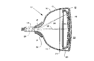
Fig. 1 shows a color CRT 10 having a glass envelope 11
Culll~Jlii,illg a rectangular faceplate panel 12 and a tubular neck 14
c, --: ' by a rect~n~ r funnel 15. The funnel 15 has an
35 internal conductive coating (not shown) that contacts an anode
button 16 and extends into the neck 14. The panel 12 c~...".i~cs a
21~6324
4 RCA 86,295
viewing faceplate or substrate 18 and a peripheral flange or
sidewall 20, which is sealed to the funnel 15 by a glass frit 21. A
Illmir- three color phosphor screen 22 is carried on the inner
surface of the faceplate 18. The screen 22, shown in Fig. 2, is a
5 line screen which includes a multiplicity of screen elements
comprised of red-emitting, ~ ,el~ e...itting and blue-emitting
phosphor stripes R, G, and B, .~ ly, arranged in color
groups or picture elements of three stripes or triads, in a cyclic
order. The stripes extend in a direction which is generally normal
10 to the plane in which the electron beams are generated. In the
normal viewing position of the embodiment, the phosphor stripes
extend in the vertical direction. Preferably, at least portions of
the phosphor stripes overlap a relatively thin, light absorptive
matrix 23, as is known in the art. Alternatively, the matrix can be
15 formed after the screen elements are deposited, in the manner
described in U.S. Pat. No. S,240,~98, issued to Fl Jr., on
Aug. 31, 1993. A dot screen also may be formed by the novel
process. A thin conductive layer 24, preferably of ~
overlies the screen 22 and provides means for applying a uniform
20 potential to the screen, as well as for reflecting light, emitted from
the phosphor elements, through the faceplate 18. The screen 22
and the overlying Alllminllm layer 24 comprise a screen assembly.
A multi-apertured color selection electrode or shadow mask 25 is
removably mounted, by conventional means, in ~l~d~,t~ led
2 5 spaced relation to the screen assembly.
An electron gun 26, shown s.' ~ic~lly by the dashed
lines in Fig. 1, is centrally mounted within the neck 14, to
generate and direct three electron beams 28 along CO.~ ,Cl~t
paths, through the apertures in the mask 25, to the screen 22.
30 The electron gun is conventional and may be any suitable gun
known in the art.
The tube 10 is designed to be used with an external
magnetic deflection yoke, such as yoke 30, located in the region of
the funnel-to-neck junction. When activated, the yoke 30 subjects
3 5 the three beams 28 to magnetic fields which cause the beams to
scan ho}izontally and vertically, in a rectangular raster, over the
2lss324
5 RCA 86,295
screen 22. The initial plane of deflection (at zero deflection) is
shown by the line P - P in Fig. 1, at about the middle of the yoke
30. For s;~ ;ly, the actual ~ul~alul~ of the deflection beam
paths, in the ~fl~cti~ zone, are not shown.
S The screen is l-f:~t--red by an elc~,ll.rhotographic
screening (EPS) process that is shown ~ ' lly in Figs. 3
through 10. Initially, the panel 12 is cleaned by washing it with a
caustic solution, rinsing it in water, etching it with buffered
hydrofluoric acid and rinsing it again with water, as is known in
10 the art. The interior surface of the viewing faceplate 18 is then
provided with the light absorbing matrix 23, preferably using the
conventional wet matrix process described in U.S. Pat.
No. 3,558,310, issued to Mayaud on Jan. 26, 1971. In the wet
matrix process, a suitable photoresist solution is applied to the
15 interior surface, e.g., by spin coating, and the solution is dried to
form a photoresist layer. Then, the shadow mask is inserted into
the panel and the panel is placed onto a three-in-one lighthouse,
which exposes the photoresist layer to actinic radiation from a
light source that projects light through the openings in the shadow
20 mask. The exposure is repeated two more times with the light
source located to simulate the paths of the electron beams from
the three electron guns. The light selectively alteTs the solubility
of the exposed areas of the photoresist layer where phosphor
materials will ~ub~ u~ ly be deposited. After the third
2 5 exposure, the panel is removed from the lighthouse and the
shadow mask is removed from the panel. The photoresist layer is
developed, using water, to remove the more soluble areas thereof,
thereby exposing the underlying interior surface of the faceplate
and leaving the less soluble, exposed areas of the photoresist layer
30 intact. Then, a suitable solution of light-absorbing material is
uniformly provided onto the interior surface of the faceplate 18 to
cover the exposed portion of the faceplate and the retained, less
soluble, areas of the photoresist layer. The layer of light-
absorbing material is dried and developed using a suitable
3 5 solution which will dissolve and remove the retained portion of
the photoresist layer and the overlying light-absorbing material,
21 ~G32~
6 RCA 86,295
forming windows in the matrix layer which is adhered to the
interior surface of the faceplate. For a panel 12 having a diagonal
~" of 51 cm (20 inches), the window openings formed in
the matrix have a width of about 0.13 to 0.18 mm, and the matrix
5 lines have a width of about 0.1 to 0.15 mm. The interior surface
of the faceplate 18, having the matrix 23 thereon, is then coated
with a suitable layer 32 of a vo1O~ili7lhl~ organic conductive (OC)
material which provides an electrode for an overlying
volatilizable, organic r' ~ nd~lctive (OPC) layer 34. The OC
10 layer 32 and the OPC layer 34 are shown in Fig. 3 and, in
c~ mtin~ltion, comprise a ph :~ c~u~ 36.
Suitable materials for the OC layer 32 include certain
quaternary ~mm~ polyelectrolytes recited in U.S. Pat.
No. 5,370,952, issued on Dec. 6, 1994 to Datta et al. Preferably,
15 the OPC layer 34 is formed by coating the OC layer 32 with a
solution containing polystyrene; an electron donor material, such
as 1,4-di(2,4-methyl phenyl)-1,4 diphenylbutatriene (hcl~ a
2,4-DMPBT); electron acceptor materials, such as 2,4,7-trinitro-9-
fluorenone (hereinafter TNF) and 2-ethylanthroquinone
20 (hereinafter 2-EAQ); and a solvent, such as toluene or xylene. A
__r ' t, such as silicone U-7602 and a plasticizer, such as
dioctyl phthalate ('~ ~,;..art~,l DOP), also may be added to the
solution. The s r?~ 1:...I U-7602 is available from Union Carbide,
Danbury CT. As shown in Fig. 4, the OPC layer 34 is uniformly
25 ele~lu~lalically charged using a corona discharge device 38,
described in U.S. Pat. No. 5,083,959, issued on Jan. 28, 1992 to
Datta et al., which charges the OPC layer 34 to a voltage within
the range of a~u,ulu~ t~,ly +200 to +700 volts. The shadow
mask 25 is then inserted into the panel 12, which is placed onto a
30 li~h~ -CA 40, shown s ' --lly in Fig. 5, and the positively
charged OPC layer 34 is exposed, through the shadow mask 25, to
light from a xenon flash lamp 42, or other light source of sufficient
intensity, such as a mercury arc, disposed within the lighthouse.
The light which passes through the apertures in the shadow mask
35 25, at an angle identical to that of one of the electron beams from
the electron gun of the tube, .Jis~ dl~;~s the i111lmin~ d areas on
.
21~2~
7 RCA 86,295
the OPC layer 34 on which it is incident. The shadow mask is
removed from the panel 12 and the panel is placed onto a first
phosphor developer 44, such as that shown in Fig. 6. The first
color-emitting phosphor material is positively triboelectrical
5 charged within the developer 44 by a triboelectric gun 46 and
directed toward the OPC layer 34. The positively charged first
color-emitting phosphor material is repelled by the positively
charged areas on the OPC layer 34 and deposited onto the
discharged areas thereof by the process known in the art as
10 "reversal" development. In reversal development,
triboelectrically charged particles of screen structure material are
repelled by similarly charged areas of the OPC layer 34 and
deposited onto the d;s~ .rb_d areas thereof. The size of each of
the lines of the first color-emitting phosphor is slightly larger than
15 the size of the openings in the light-absorbing matrix, to provide
complete coverage of each opening and a slight overlap of the
light-absorbing matrix material ~u~ 1ing the openings. The
panel 12 is then recharged using the above-described corona
discharge :irr!'r~ltllC A positive voltage is established on the OPC
20 layer 34 and on the first color-emitting phosphor material
deposited thereon. The light exposure and phosphor development
steps are repeated for each of the two remaining color-emitting
phosphors. The size of each of the lines of the other two color-
emitting phosphors on the OPC layer 34 also is larger than the size
25 of the matrix openings, to ensure that no gaps occur and that a
slight overlap of the light-absorbing matrix material surrounding
the openings is provided. The resultant screen 22 is shown in
Fig. 7.
The three light-emitting phosphors are fixed to the above-
30 described OPC layer 34 by conf~ting the PhsF with a
suitable fixative that is electrostatically charged by an
U~lic spray gun 58, s~ ly shown in Fig. 8. Suitable
fixatives include such solvents as acetone; amyl acetate; butyl
acetate; methyl isobutyl ketone (MIBK); methyl ethyl ketone
35 (MEK); toluene; and xylene; and polymeric solutions, such as
21~32~
8 RCA 86,295
acrylic resiD dissolved in MIBK; and pOly-A'~'~~ ' yl styrene
(AMS) dissolved in MIBK.
Any one of the above oned solvents may be used to
fix the phosphors to the underlying OPC layer 34. The preferred
S ele~L.~LdtiC spray gun is an AEROBELLTM model, available from
ITW Ransburg, Toledo, OH. The clc~,LIo~ld~ic gun provides
negatively charged droplets of uniform size which wet the
ph r h ~ and the underlying OPC layer 34, without moving the
P~ r As shown in Fig. 8, the panel 12 is oriented with the
10 OPC layer 34 and the phosphors directed downwardly toward the
electrostatic gun 58. The downward orientation of the panel
prevents any large droplets forming on the gun from dropping
onto the screen 22 and moving the phosphors. The polystyrene
used in the OPC layer 34 is completely soluble in amyl acetate,
15 butyl acetate, MIBK, toluene and xylene, and partially soluble in
acetone, all the forrner having a boiling point within the range of
100 to 150C. MIBK, however, is preferred because it dissolves
the polystyrene of the OPC layer 34 more slowly than the other
solvents. The phosphors are then filmed to provide a layer which
20 forms a smooth surface over the screen 22 onto which an
evaporated Al ' ~m layer is deposited. The filming may be a
conventional emulsion filming or the dry filming described in the
above-cited U.S. Pat. No. 5,028,501, or the filming may comprise
an elccllo~ldlically deposited polymeric solution, as described
2 5 below. After filming, the screen assembly is Alllmini7~d and then
baked at a t~,-..p~,ldlu.e of about 425C. for about 30 minutes, to
drive off the volatilizable cc~ctifll~nts of the screen assembly.
The fixative MIBK is preferred with the present Cl~ L~lic
spray system because the phosphors are sllbstAntiAlly completely
3 0 encArs~ t- d within the dissolved poly~y.. .e based OPC layer
34, as ghown in Fig. 9, without distorting the phosphor lines or
cracking, or otherwise adversely affecting, the structure of the
OPC layer. While filming of the . l~t(-d phosphors is not
required, it is, nevertheless. desirable in order to provide a
3 5 smooth surface on which to deposit the evaporated aluminum
layer.
21~32~
9 RCA 8G,295
The preferred filming material solution is an acrylic resin
dissolved in MIBK. Good results have been obtained using a resin,
available from Pierce and Stevens, Buffalo, NY, eomprising about
90 wt. % of polymethyl ~ ,lha~,lyL.t~" 9 wt. % of isobutyl
S Ill~lL~ late, and the balance being the plasticizer DOP and
nitroc~ )s~ The resin solids comprise about 3 to 10 wt. % of the
filming solution. Another suitable resin is poly-al~ yl
styrene (AMS) dissolved in MIBK. The AMS c~..,.l..;~es about 3 to
15 wt. %, and preferably 3 to 10 wt. %, of the solution. AMS is
10 commercially available as Herculite 240, from Hercules, Inc.,
Wilmington, DE.
In another embodiment of the present invention, shown in
Fig. 10, the phcsl ~. are fixed and filmed cim~l ~ Iy, i.e., in
one-step, using B-67 acrylic resin dissolved in MIBK. B-67 is
15 available from RHOM and HAAS, Philadelphia, PA. Screen samples
were prepared having film thickr-~-- ranging from 5 to 15
microns (u). A 10 u thick B-67 acrylic film 60 produced smooth
coverage of the phosphors. The thickness of the film 60 is
dct~,llllillcd by the co..~,~.llldlion of the solid resin in the solution
20 and by the number of passes made across the phosphor screen by
the elc~ lalic gun 58.
An alternative to the above described one-step method of
fxing and filming is to fix and film in separate steps. The fixing
step is accomplic~-d by electrostatically spraying a thin coating,
25 not shown, of a solution comprising I to 5 wt. % of B-67 acrylic
resin dissolved in MIBK, onto the phosphors of the screen 22.
Then, the fixed screen is overcoated by elc~ ldlically spraying a
solutio~ comrrieing 5 to 15 wt. % of the B-67 acrylic resin, also
dissolved in MIBK, onto the fixed screen, to provide a filming
3 0 layer, also not shown, having a thickness within the range of
about 5 to 10 u. It has been ~l~t~ ~mi~ d that thermal
d~colll~Josilion of the acrylic B-67 begins at 205C. and the
material bakes out rapidly at 336C. This rapid decomposition of
the filming material is believed to cause ollt~ccing that produces
3 5 blisters in the ~ lminllm layer during screen bake. It is further
believed that the blister problem can be solved by adjusting the
' ~ 21~32~
RCA 86,295
screen bake pa.~r~.~t~ to provide a slower, i.e.. Ionger, bake
cycle, to permit the gas evolved from the decomposition of the
volatilizable materials to pass through the aluminum layer
without causing it to blister. However, in . - ,.r~ g screens
5 by the EPS process, it is desirable to decrease the screen
processing time; thus, other filming materials were investigated.
One such material is AMS which bakes out cleanly at 440C.
and decc,---l,os~s more slowly than B-67, so that blisters are less
likely to form. A solution of 5 wt. % AMS dissolved in MIBK was
10 electrostatically sprayed onto the F~ r to fix them to the OPC
layer 34. The fixing layer had a thickness of one micron. The
fixing layer was overcoated with a 10 u thick filming layer formed
by a solution of 15 wt. % AMS dissolved in MIBK. The panels
were ~ rnini7~d and baked, and were free of blisters.