Note: Descriptions are shown in the official language in which they were submitted.
- `-- ` 2156~65
CLIP AND METHOD THERFOR
Field of the Invention:
The present invention pertains to electrical grounding clips.
R~çkFround of the Invention:
Electronic devices are well known that include electronic circuits
10 mounted on electronic circuit boards. It is important that these
electronic circuits are adequately grounded for proper operation. One
method of grounding circuits is to provide a relatively large electrically
conductive member as a ground plane. Ground conductors of the
electronic circuits are connected to this conductive member to effect
15 circuit ground. One electrically conductive member that is often used in
electronic devices is an electrically conductive layer on the interior
surface of the device's housing.
A di~lculty experienced by electronic device manufacturers is
providing an effective ground connection between the electronic circuit
2 0 and the large conductive element which is reliable and inexpensively
assembled. Providing an electrical connection between the circuit board
and the ground member using wires and soldier increases the assembly
time, and the overall complexity and cost of manufacturing the
electronic devices. Known me~h7.nic~1 connectors contacting surfaces on
2 5 the circuit board and ground member are expensive and challenge
assemblers attempting to consistently insure that electrical connection
is made.
Accordingly it is desirable to provide an electrical connector
which is readily assembled in an electronic device and reliably connects
3 0 the circuit board to the ground member.
- 1 -
` ` 21S6~G5
Brief Description of the Drawings
FIG. 1 is a front perspective view Illustrating a clip;
s
FIG. 2 is a rear perspective view illustrating the clip from an
opposite direction of FIG. 1;
FIG. 3 is a side elevational plan view illustrating the clip of FIG.
10 1;
FIG. 4 is a bottom plan view illustrating the clip according to
FIG. 1;
FIG. ~ is an exploded perspective view illustrating a radio
telephone including a clip;
FIG. 6 is an enlarged exploded perspective view illustrating a
rear housing section assembly, clips, and a printed circuit board;
FIG. 7 is a fragmentary cross-sectional view of the front housing
section, back housing section printed circuit board taken along plane
VII-VII in FIG. 11;
2 5 FIG. 8 is an enlarged exploded perspective view illustrating the
back housing section and clips;
FIG. 9 is a bottom perspective view illustrating the front housing
section of the radio telephone of FIG. 1;
FIG. 10 is a bottom perspective view illustrating the RF circuit
board of FIG. 1.
FIG. 11 is a top perspective view illustrating the assembled radio
3 5 telephone;
- 2 -
215646~
FIG. 12 is a fragmentary perspective view illustrating a printed
circuit board, clips, and back housing section cut along plane XII-XII in
FIG. 11; and
FIG. 13 is a fragmentary cross-sectional view illustrating the
radio telephone components cut along plane XII-XII in FIG.11.
Detailed Description of the Drawings
A clip 100 (FIG. 1) is manufactured of a resilient conductive
material. The clip includes three contact surfaces 116, 118, and 122
which are spaced from one another for engagement with three mating
surfaces of a device in which the clip is used. Each of the contact
l 5 surfaces is oriented to make contact with a mating surface on the device
that is in a different plane. The clip is configured to impart a
predetermined force in a direction (E, D, and F) substantially
orthogonal to the plane of each contact surface when the clip is
assembled in the device. The clip can therefore be readily assembled in
2 0 an electronic device and provide a secure contact with mating surfaces
in different planes thereof to facilitate assembly and reliable electrical
interconnection of electrically conductive components.
Clip 100 (FIG. 1) includes a bow 102 connected to a central plate
104 by a first elbow 106. A second elbow 108 (FIG. 2) interconnects a
central plate 104 with arm 110. Arm 110 includes a barb 112 (FIG. 3)
which functions as an att~çhment mel~h~ni~m for the clip. Although the
illustrated att~hment me~h~ni~m is an integrally formed barb, it may
be an integral dimple, a separate fastener, or any other suitable
connector. A finger 114 extends from an end of arm 110 remote from
3 0 first elbow 106. First elbow 106 and second elbow 108 extend from
opposite ends of central plate 104 such that the clip is generally S-
shaped in profile. Bow 102 includes a contact surface 116 (FIG. 1) at
the apex of the clip, a contact surface 118 (FIG. 2) at the leftmost
projecting point of bow 102, and a contact surface 120 (FIG. 4) at the
2156~65
bottom location in first elbow 106. Finger 114 also includes a contact
surface 122 at the end thereof.
Clip 100 is manufactured of a beryllium and copper alloy that is
one-half hard and heat treated at approximately 600 F for 2 hours.
S However, the clip may be manufactured of other suitable electrically
conductive, resilient materials, such as other copper alloys, an
electrically conductive polymeric constructions, or the like. The clip is
resilient to resist movement at each of the contact surfaces but allows
some collapsing of the clip to conform to marginally different volumes.
l 0 Additionally, the configuration of the clip provides a predetermined
force at each of the contact surfaces in a direction tangential to each of
the contact surfaces to push the contact surfaces against the device
surfaces thereby m~kinE a reliable electrical connection at the contact
surfaces. The clip is electrically conductive to electrically interconnect
1 S all of the contact surfaces that it contacts.
The clip has a thickness of between .05 millimeters (mm) and 1.1
mm, and in a reduction to practice had a thickness of approximately .08
mm. The bow 102 includes a top segment having a radius R1 between
.25 mm and .35 mm, and in the reduction to practice had a radius of
approximately .32 mm through an arc of approximately 70.9. The
intermediate segment of the bow has a radius R2 between 2 mm and 4
mm, and in the reduction to practice, had a radius of approximately
2.96 mm in an arc of approximately 57.9 . First elbow 106 has a first
segment with a radius R3 that is between .25 mm and .75 mm, and in
the reduction to practice, had a radius of approximately .59 mm through
an arc of approximately 55. First elbow 106 has a second segment
having a radius R4 between .25 mm and 85 mm, and in one reduction to
practice had a radius of approximately .62 mm. through an arc of
approximately 97.4. The second elbow 108 has a radius between .25
mm and .55 mm, and in the reduction to practice has a radius of
approximately .48 mm through an arc of approximately 187.4. The
finger has a radius between .10 mm and .5 mm, and in the reduction to
practice had a radius of .28 mm through an arc of approximately 148.3.
The configuration is such that contact surfaces 116, 118, 120 and 122
3 S are in different planes in the at rest condition illustrated in FIGs. 1-4.
- ` 21~646~
A radio telephone 530 (FIG. 5) employing clips 100 includes a
front housing section 532 and a rear housing section 534 which are
interconnected to form an outer casing rlefining an interior volume. A
logic circuit board 536 has a display lens 539, an opening 540 for receipt
S of a vibrator assembly 542, a miGrophone 544, a speaker 546, and other
electronic circuitry not specifi~lly shown or referenced, mounted
thereon. A slider wéb 548 is positioned between logic circuit board 536
and a radio frequency (RF) circuit board 550. RF circuit board 550 has
electronic circuitry (not shown) assembled thereon. The RF circuit
1 0 board 550 is sandwiched between stops 994 (FIG. 9) on front housing
section 532 and rear housing section 534, the stops holding the RF
circuit board 550 in position when the radio telephone is assembled.
The front housing section 532 and rear housing section 534 enclose logic
circuit board 536, slider web 548, and RF circuit board 550 when fully
1 5 assembled. Clips 100 are supported in the radio telephone such that
they exert a force against electrical conductors on the rear housing
section 534, the front housing section 532, and the printed circuit board
550, thereby m~king a reliable electrical connection between conductive
surfaces of these parts, as described in greater detail herein below.
2 0 Radio telephone as used herein refers to cellular telephones,
portable telephones, or cordless telephones. Although a portable radio
telephone 530 is illustrated, the clips 100 may be advantageously
employed in other electronic devices such as land line telephones,
radios, pagers, or any other electronic appliance. Accordingly, "device"
2 5 as used herein refers to all such electronic appliances and their
equivalents.
Rear housing section 534 (FIG. 6) includes rear housing section
snaps 660 positioned at locations spaced around the perimeter of rear
housing section 534. The rear housing section snaps 660 are all
3 0 substantially identical. Each rear housing section snap includes a
resilient arm 762 (FIG. 7) extending outwardly from the rear housing
section platform 764 at an opening 766. A wedge 768 projects from a
distal end of arm 762. The wedge 768 includes a top surface 770 that
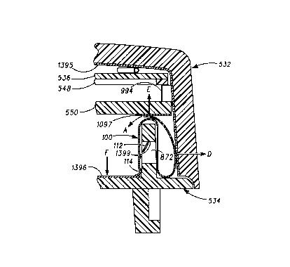
slopes toward the apex 772 of arm 762.
21~ 16~i
The rear housing section 534 (FIG. 6) also includes mounting
posts 668 at spaced locations around the perimeter thereo The
mounting posts 668 include a generally rectangular planar body 870
(FIG. 8) having a central opening 872. Central opening 872 is for receipt
S of barb 112 (FIG. 3). The central planar member extends between
protuberances 874 and 876. The mounting posts 668 (FIG. 6) are
preferably located adjacent the back housing section snaps 660, and
may be positioned on opposite sides of one or more of these snaps.
A positioning post 578 (FIG. 5) on back housing section 534
l 0 provides a guide mech~niRm for locating logic circuit board 536 and RFcircuit board 550. For this purpose logic circuit board 536 includes an
opening 580 and RF circuit board 550 includes opening 682 (FIG. 6).
Openings 580 and 682 receive positioning post 578. Positioning post
578 is located such that when the post is received in openings 580 and
l 5 682 while the circuit boards are properly oriented with respect to thefront and back housing section sections 532 and 534, the printed
circuit boards are aligned for full assembly of the telephone housing
section sections.
Front housing section 532 (FIG. 5) includes a speaker opening
534, a display lens 538, and key pads 584 (only some of which are
numbered). Key pads 584 are positioned to actuate popple switches
586 on logic circuit board 536 when the key pads are pressed. A
speaker 546 is supported behind speaker opening 534 in front printed
circuit board 536. A slide switch 588 for discharging memory cards is
positioned inside front housing section 532 and tracks on slider web
548.
The front housing section 532 also includes arcuate staples 990
(FIG. 9) extending outwardly from the sidewalls 992 and 993 of the
front housing section 532. Stops 994 project from the inside surface of
sidewalls 992 and 993.
The front housing section 532 and the back housing section 534
are manufactured of conventional materials and by a convention
manufacturing~rocess for electronic devices. For example, they may be
an integrally molded of an organic polymer. An electrically conductive
3 S layer 1395 (FIG. 13) is supported on the interior surface of the front
6 5
housing section 532. An electrically conductive layer 1396 is .simil~rly
supported on the interior surface of back housing section 634. The
electrically conductive layers 1395 and 1396 are manufactured of a
conductive material, such as a metal member mounted near the interior
S of the housing section, a metallized film applied directly to the interior
of the housing section using a suitable conventional process, or any
other suitable conductor which covers a relatively large surface area.
Layers are preferably a metallized film, or surface materiel, applied to
the interior surface of the front housing section 532 and back housing
1 0 section 534, as this provides a light-weight and relatively small volume
circuit ground.
Contacts 1097 (FIG. 10) are supported at predetermined
locations of the perimeter of the RF circuit board 550. Contacts 1097
are formed on the circuit board by conventional printing processes.
These contacts are connected to ground conductors (not shown) on the
RF circuit board. The ground conductors are in turn connected to
termin~l~ of integrated circuits (not shown), impedance devices and the
like, mounted on the printed circuit board which are connected to circuit
ground.
2 0 To assemble a grounding clip 100 (FIG. 8) to a mounting post
668, the grounding clip is positioned above planer member 870 with the
barb 112 aligned with opening 872. First elbow 106 (FIG. 3) and finger
114 have curved surfaces which contact the top of wall 668. These
curved surfaces slide over corners of post 668 and push central plate
104 and arm 110 away from one another such that the mounting wall is
received therebetween. Barb 112 slides over wall 668 until it moves
over recess 872. The barb will then snap into opening 872 and the clip
is held securely on the wall as shown in FIG. 13. In this position, finger
114 is pressed against the metallized inner layer 1396 of the back
housing section and the pressure exerted by barb 112 against wall 1399
slightly compresses finger 114.
The logic circuit board 106 is assembled into front housing
section 532. The circuit boards 536 and 550 are positioned at
predetermined locations in this housing section by positioning post 578
3 5 through aperture 580 and aperture 682 (FIG. 6). The logic circuit board
- 7 -
21S~6~
550 is also positioned by web 112, which hold the logic board within the
front housing section 532, and slide switch 588, received in aperture
599 in the front housing section 102. The RF circuit board is then
positioned over the web, such that post 578 is received in aperture 682
(FIG. 6).
The front housing section 532 (FIG. 6) and back housing section
534 are interconnected after the logic circuit board 536 and RF circuit
board 550 are positioned in the front housing section. The back
housing section snaps 660 engage staples 990 (FIG. 9) on front housing
1 0 section 532 to hold these sections together. The front housing section532 preferably includes an integral cylinder 998 for receipt of the
positioning post 578 of the back housing section. An additional
~lignment mech~ni~m may be provided by a guide member 677 (FIG. 6)
on back housing section 534, which slides into a rail 979 in front
1 S housing section 532.
The top surface 770 (FIG. 7) of wedge 768 slides against the
staple 990 to push arm 762 inwardly and the staple deflects outwardly.
After the wedge slides past the staple, the resilient arm pushes the
wedge over the staple to the position illustrated in FIG. 7. In this
2 0 position, the bottom surface of the wedge rests against the top surface
of the staple. To separate the snap connector from the staple, an
implant is inserted through flexible arm opening 766 and is used to
separate the wedge and the staple.
When the back housing section 534 is assembled to the front
2 S housing section 532, the bow 102 is pushed downwardly by the RF
circuit board moving in direction B (FIG. 12) and the back housing
section exerting a force in direction C. This forces bow 102 to move in
directions A and D. The bow 102 arcs outwardly in direction D at
surface 116 (FIG. 1) providing a firm engagement with the inner surface
3 0 1395 (FIG. 13) of front housing section 532. When the bow abuts with
the inside surface of the front housing section, the contact surface 116 of
the bow 102 will push firmly against the RF circuit board contact 1097
and tend to move in direction A. The RF circuit board contact 1097
abuts with surface 116. The barb 112 pushes finger 114 in direction F
3 S at contact surface 122 thereby, providing a firm connection with
- 8 -
21~S~5
conductor 1396. Thus, the conductor contacts the circuit board contact
1097, the conductive layer 1395 on the inner surface of the front housing
section 532, and the conductive layer 1396 on the inner surface of the
back housing section 534. This provides a secure reliable ground
5 connection between the front housing section ground layer, back housing
section ground layer, and the printed circuit board ground conductor,
thereby effecting a reliable circuit ground connection and avoiding the
circuit destruction do to improper grolln(ling.
Because barbs 112 (FIG. 13) of clips 100 are pressed into the top
l 0 surface of opening 872 by arms 110 when fingers 114 push against
electrically conductive layer 1396, layer 1396 is held firmly against
contact surface 122 (FIG. 2). The stops 994 (FIG. 13) on the front
housing section 532 hold the RF circuit board electrically conductive
layer 1395 against the clip surface 116 (FIG. 1). The clip 100 is thus
1 5 pinched between the back housing section 534 (FIG. 13) and the RF
circuit board. This pin~hing of the clip presses contact surface 118
(FIG. 2) of the clip outwardly against the front housing section
conductive layer. The clip thus exerts a force against the conductive
layers on front housing section 532, the back housing section, and the
20 RF circuit board, thereby m~king electrical connection with conductors
in three differently oriented planes.
The clips are aligned with the contacts on the RF circuit board by
the position of mounting posts, the ~lignment post 378, and sidewalls
of the front housing section 532. The fully assembled radio is
25 illustrated in FIG. 11.
Thus it can be seen that a clip is disclosed which is readily
assembled into a device. The clip is resilient, such that it makes
contact the inside surfaces in different planes, and the movement of the
bow allows the clip to reliable contact surfaces in marginally different
3 0 volumes. The contact may thus be used to provide a ground connection
in electrical devices such as radio telephones, pagers, electronic
appliances, and the like with a high degree of confidence.