Note: Descriptions are shown in the official language in which they were submitted.
~~ a~~~~
PATENT
ACTIYE DISCHARGE CIRCUTT FOR CHARGED CAPACITORS
Background of the Invention
This invention relates generally to electronic power supplies and in
particular to a
circuit for discharging charged capacitors in a power supply after a.c. power
is removed.
The typical d.c. power supply used to supply d.c. voltages from an a.c. line
voltage
operates by converting the a.c. line voltage level to a desired a.c: voltage
level using a
transformer, rectifying the a.c. voltage to a pulsating d.c. voltage with
semiconductor
diodes, and filtering the pulsating d.c. voltage with capacitors to obtain the
smoothed d.c.
voltage. Capacitors) by virtue of their ability to store large amounts of
electrical charge,
function as filters by alternatively storing the charge from the peaks of the
pulsating d.c.
voltage which functions as the charging voltage and then releasing the charge
between the
peaks in the manner of a reservoir.
Capacitors have the ability to retain a substantial amount of stored charge
long
after the a.c. line power is removed if there is no path for the charge to
bleed off,
presenting a safety hazard to persons who may accidentally come in contact
with the
power supply. To address this concern) various techniques of discharging the
capacitors
have been devised. The simplest technique involves coupling a bleeder resistor
in shunt
across the capacitor. After the charging voltage is removed, the capacitor
discharges
through the bleeder resistor which dissipates the stored charge as heat. The
disadvantages
of the continuously-coupled bleeder resistor are that it continually
dissipates energy,
resulting in wasted energy which appears as heat build-up in the power supply
and heavier
duty components must be used to dissipate the heat continuously. An improved
technique
is to connect a relay in series with the bleeder resistor with the relay coil
coupled to the
a.c. line voltage in such a way that the relay contacts close and couple the
bleeder resistor
to the capacitor when the power supply is switched off. In this way, no power
is
dissipated in the bleeder resistor during the normal operation of the power
supply. Relays
-1-
that are capable of this task.tend to be bulky and expensive and) as
mechanical switching
devices, may not achieve adequate reliability where there is a concern for
safety.
Semiconductor switches that perform the function of the relay have lacked a
simple means
of detecting the removal of the charging voltage from the capacitor when the
power
supply is switched off. Therefore, it would be desirable to provide an active
discharge
circuit using a relatively small number of inexpensive semiconductor
components that is
capable of detecting the removal of charging voltage and responsively coupling
an energy
dissipating element across the filter capacitor to facilitate its safe
discharge.
Summarv of the Invention
In accordance with the present invention, an active discharge circuit is
provided,
which couples an energy absorbing element across the filter capacitors in a
power supply
upon sensing the removal of the charging voltage. The active discharge circuit
is
implemented with a small number of inexpensive components, minimizing
component cost,
circuit complexity, and physical volume while providing for the safe discharge
of
potentially hazardous amounts of charge stored in the capacitors. Because the
energy
absorbing element is decoupled from the capacitor during norrnal operation of
the power
supply) no energy is dissipated as wasted heat.
One object of the present invention is to provide an active discharge circuit
which
detects the removal of charging voltage and responsively couples an energy
dissipating
element across a capacitor.
Another object of the present invention is to provide an active discharge
circuit
which employs a small number of inexpensive, semiconductor components to
detect the
removal of charging voltage and responsively discharge the filter capacitor
through an
energy dissipating element.
An additional object of the present invention is to provide a detector which
detects
the removal of the pulsating d.c. charging voltage from a filter capacitor and
sends a signal
-2-
~I~~5~2
to a semiconductor switch which responsively couples a bleeder resistor across
the filter
capacitor to facilitate its discharge.
Other features, attainments) and advantages will become apparent to those
sldlled
in the art upon a reading of the following description when taken in
conjunction with the
accompanying drawings.
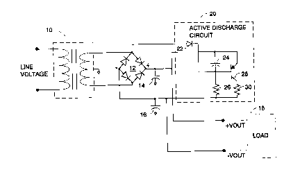
Brief Descrintion of the Drawings
The single FIGURE is a circuit schematic diagram of an active discharge
circuit in
accordance with the present invention.
l0 Detailed Descrintion of the Invention
Referring now to the FIGURE, there is shown a circuit schematic of the present
invention as applied in a conventional power supply. A transformer 10 has a
primary
winding coupled to an a.c. (alternating current) line voltage and a secondary
winding
magnetically coupled to the primary winding to step up or step down the a.c.
line voltage
to a desired voltage level according to the primary to secondary turns ratio.
The
secondary winding has a center-tap and the center-tap is coupled to circuit
ground. The
secondary winding is further coupled to a full-wave rectifier 12 which
converts the a.c.
voltage developed across the secondary winding to a pulsating d.c. voltage at
the
terminals labeled + and -. Capacitors 14 and 16 are coupled to the + terminal
and -
terminal respectively of the full-wave rectifier 12 and function as filters to
produce a d.c.
voltage at a pair of output terminals labeled +VOUT and -VOUT. A load 18 is
coupled to
the terminals +VOUT and -VOUT.
Because the full-wave rectifier 12 delivers a pulsating d.c. voltage, which
functions
as the charging voltage for the capacitors 14 and 16, at twice the line
frequency, the
capacitors 14 and lb must have enough capacitance to meet a desired output
ripple level
when the power supply is delivering a predetermined amount of current to a
load.
Capacitance is measured in Farads which is the amount of charge stored per
volt
-3-
. ~~~~~4~
according to the formula C = [ q / V ] where q is the amount of charge as
measured in
coulombs and V is the voltage across the capacitor. Because the power supply
must
deliver an output current I between peaks of the pulsating d.c. charging
voltage, the size
of the capacitor is' generally governed by the maa~imum amount of tolerable
"ripple" at the
output which is the result of voltage drop by the steadily discharging filter
capacitors
between the peaks of the pulsating voltage. The amount of ripple is generally
governed by
the equation C = [ (I * t ) / Vr ] where I is the current delivered to the
load, t is the time
between peaks of the charge voltage) and Vr is the ma»imum acceptable ripple
voltage.
As the required current I delivered to the load increases, the relative size
of the capacitor
i0 must be increased to store and release more charge in order to maintain the
desired ripple
voltage. It is common for power supply filter capacitors to have the ability
to store a
substantial amount of charge in response to the above mentioned design
considerations.
If the voltages +VOUT and -VOUT are substantially higher than limits set by
either engineering practice or by industry regulation, typically a value of 60
volts d.c., a
safety concern arises. A common scenario to guard against involves a power
supply on a
service bench for repair which has been removed from its protective enclosure)
and has
had the load 18 disconnected firom its output terminals. The capacitors 14 and
16, with no
load to deliver their charge q to, may retain hazardous voltage levels for
long periods of
time after the a.c. line voltage has been removed.
An active discharge circuit 20 applied to the power supply circuit provides a
means
of discharging the capacitors 14 and 16 when the a.c. line voltage is removed
which does
not depend on the presence of a load 18 to operate. A diode 22 with an anode
coupled to
the secondary winding of transformer 10 provides a rectified d.c. voltage that
indicates the
presence of the a.c. voltage developed at the secondary winding. A cathode of
the diode
22 is coupled to the junction of a capacitor 24 and a resistor 26 which are
disposed in
series between the +VOUT terminal and the -VOUT terminal. The junction of
capacitor
24 and resistor 26 is further coupled to a base of a bipolar p-n-p transistor
28. Transistor
-4-
~~~~5~~
28 is implemented as a semiconductor switch with the base functioning as a
control input)
a collector coupled to the +VOUT terminal, and an emitter coupled to a
resistor 30 which
is in turn coupled to the -VOUT terminal. It will be obvious that an n-p-n
bipolar
transistor, a field effect transistor, or other semiconductor switching device
can be
. employed as a semiconductor switch with appropriate attention to apply the
particular
device technology by one sldlled in the art.
When the power supply is operating) a.c. voltage is present at the secondary
winding of thenransformer 10. The a.c. voltage is re~ed by the diode 22 and
maintains
the voltage across the capacitor 24 and the base-emitter junction of the
transistor 28 at
substantially zero volts. Transistor 28 is therefore off during this time and
no current
flows through the emitter-collector junction to the resistor 30.
The combination of the diode 22, capacitor 24, and resistor 26 form a detector
that
generates a signal responsive to the removal of the a.c. voltage. At the
moment that a.c.
power is removed from the power supply, the pulsating d.c. charging voltage
disappears
and capacitor 24 begins to charge through the resistor 26. The time constant
of the
capacitor 24 charged by resistor 26 is substantially longer than the period of
the pulsating
d.c. charging voltage so that the voltage across capacitor 24 remains
essentially zero
between peaks of the charging voltage to prevent the switch finm closing
during the
nomsal operation of the power supply. For a 60 hertz power line signal, the
period of the
pulsating d.c. charging voltage is 16.7 milliseconds. In the preferred
embodiment,
+VOUT is 65 volts, -VOUT is -65 volts, capacitor 24 is 100 microfarads) and
resistor 26
is 300,000 ohms. Capacitor 24 charges above 0.6 volts in approximately 140
milliseconds
after a.c. power is removed, thereby turning on transistor 28) and allowing
current to flow
through the emitter-collector junction of the transistor to the resistor 30,
allowing the
capacitors 14 and 16 to discharge through resistor 30 which has a value of
10,000 ohms in
the preferred embodiment. This invention as shown is designed for applications
in which
the capacitor 14 has a capacitance equal to or larger than that of the
capacitor 16. By
-5-
~1~~542
requiring the capacitor 14 to have higher capacitance, it is assured that the
capacitor 16
discharges first, leaving the capacitor 14 to finish discharging through the
diode bridge 12
and the transformer 10 center tap to ground thereby completely discharging the
power
supply. Alternatively, if the capacitor 16 is larger than the capacitor 14, it
will be obvious
to implement the active discharge circuit 20 to operate against the capacitor
16 rather than
the capacitor 14 by coupling the active discharge circuit to the -Vout rail,
reversing the
relevant polarities and substituting an n-p-n transistor 28 for the p-n-p
shown in the
commercial embodiment.
Discharging a capacitor involves dissipating its stored charge, usually in the
form
of heat energy, by an energy dissipating element. In the preferred embodiment,
the energy
dissipating element is the resistor 30. The transistor 28 is operated as a
switch by
saturating the base circuit and turning the transistor 28 fully on in a
'saturated' condition.
Because the transistor 28 is saturated, the voltage drop across the emitter-
collector
junction is relatively low and a substantially small portion of the energy is
dissipated in the
transistor 28. The capacitors 14 and 16 are each 1,700 microfarads. The
discharge time t
of the capacitors 14 and 16 is governed by the equation t = [ (C * V) / I ]
where C is the
total capacitance in farads, V is voltage across each capacitor and I is the
discharge
current. Here,
t = [( 3,400 microfarads * 65 volts ) / 13 milliamperes ]
t = 17 seconds
The discharge time of 17 seconds is within the desired time limit to safely
discharge the
capacitors 14 and 16.
It will be obvious to those having ordinary sldll in the art that many changes
may
be made in the details of the above described preferred embodiments of the
invention
without departing from the spirit of the invention in its broader aspects. For
example,
the active discharge circuit may be applied to single-ended power supplies
that have only a
+VOUT or a -VOUT output. Furthermore, the active discharge circuit may be
applied in
-6-
~1~~54~
power supplies where the size of the filter capacitor and the amplitude of the
voltages
+VOUT and -VOUT are not equal simply by using separate discharge circuits for
each
filter capacitor while utilizing common monitoring of the a.c. secondary
voltage. Finally,
the transistor 28 can be applied as the energy absorbing element, rather than
the resistor
30, by injecting a predetermined amount of current into the base of the
transistor 28,
which allows the transistor 28 to operate in its Iinear region and operate as
a current
source or sink. Therefore) the scope of the present invention should be
determined by the
following claims.
io
20