Note: Descriptions are shown in the official language in which they were submitted.
" 2156~84
19500-11479
Daigle/~ P~le~ - 'Ang
ELECrROLUMlNESCENT EDGE CONNECT-COMPOSITE LAMP/STRIP
AND METHOD OF MA~NG THE SAME
BACKGROUND OF THE II~VENTION
This invention relates generally to electroluminescent lamps and more particularly to
an improved method and structure for making electrical connections to an electroluminescent
l0 lamp from only one side of the lamp.
Electroluminescent lamps are generally constructed as l~min~ted or layered structures.
Electroluminescent lamps function by application of an electrical potential to two conductive
layers separated by an electroluminescent layer, which may comprise electroluminescent
particles fixed in a resin binder.
Electroluminescent lamps have been modified to provide a lighted watch dial, as
disclosed in U.S. Patent No. 4,775,964 issued October 4, 1988 to Alessio et al and assigned
to the present assignee. While it is easy to make one of the electrical contacts to the back
electrode comprising a conductive area on the underside of the electroluminescent watch dial,
it is more difficult to make the other electrical contact to the front electrode, since this is a
20 conductive layer which is embedded between other layers. Therefore, it has been necessary to
either omit a part of the electroluminescent material to expose the front electrode, as shown in
21~658~
-
19S00-11479
Daigle/l ~ s-~ ~ 'Ang
the aforesaid Alessio et al patent, or to provide a special overlap area extending beyond the
normal periphery of the lamp.
An improved electroluminescent watch dial support and connector assembly is shown
in U.S. Patent No. 5,265,071 issued November 23, 1993 and assigned to the present assignee,
5 employing special tabs extending beyond the dial periphery for making electrical contact.
However, it would be desirable to make electrical contact to both of the electroluminescent
electrodes from any location on the back of the EL lamp without regard to the location of the
lamp periphery.
It should be recognized that wherever electroluminescent material is miC~in~, there is
o an objectionable dark spot on the lamp, since there are no electroluminescent particles to
luminesce. In the case of an electroluminescent watch dial, it is preferable that the entire area
used for observing the timekeeping numbers or other indicia be lighted without the presence
of such a dark spot. However, there are some areas near the center of the watch dial in
which a dark spot may be permitted without in~elre~ g noticeably with the aesthetic qualities
15 of the timepiece. In U.S. Patent No. 5,346,718 issued September 13, 1994 and assigned to
the present assignee, a process of manufacturing an electroluminescent watch dial is disclosed
in which the dark spot could be located wherever desired, and which also permits electrical
connection to both front and back electrodes from any location on the rear of the
electroluminescent watch dial. Nonetheless, it would be desirable to make electrical contact
20 to both of the electroluminescent electrodes from any location on the back of the EL lamp
2156584
19500-11479
Daigle/Ledesma/Ang
with the dark spot minimi7ed to virtual nonexistence.
Accordingly, it is the object of the present invention to provide an improved
electroluminescent lamp and method of making the same in which electrical contacts are
permitted from any location on one side of the lamp with the dark spot minimi7ecl to near
elimin~tion.
SUMMARY OF THE ~VENTION
Briefly stated, the invention in its broadest form is practiced by providing a transparent
substrate with a first conductive layer thereon, the first conductive layer terminating in a first
edge, depositing an electroluminescent layer on the first conductive layer, depositing a first
inc~ tin~ layer on the electrolllminescent layer, depositing a second conductive layer on the
first in~ul~ting layer, the second conductive layer having a second edge spaced from the first
edge, depositing a second in~ ting layer on the second conductive layer, the second
insulating layer having an insulating end extending around and enclosing the second edge of
the second conductive layer, and depositing a film of conductive material on the second
insulating layer, a conductive end of the film extending around the insulating end and making
electrical contact with the first conductive layer.
DR~W~GS
The invention, both as to org~ni7~tion and to method of practice, together with further
215658~
..
19500-11479
Daigle/l ~ 'Ang
objects and advantages thereof, will best be understood by reference to the following
specification, taken in connection with the accompanying drawings, in which:
Fig. 1 is a top view with respect to the front electrode terminals of an
electroluminescent lamp strip showing the outlines of a triangular and rhomboid dial cutouts,
Fg. 2 is an enlarged side elevational view in cross section of the electroluminescent
lamp strip where the cross section is along lines n-lI of Fig. 1,
Fig. 3 is an enlarged side elevational view in cross section of the electroluminescent
lamp strip where the cross section is along lines m-m of Fig. 1,
Fig. 4 is an enlarged side elevational view in cross section of the electroluminescent
lamp strip where the cross section is along lines ~V-IV of Fig. 1,
Fig. 5 is a top view with respect to the second in~ ting layer of an
electroluminescent lamp strip with the front electrode terminal omitted, showing an electrical
contact area of the front electrode terminal,
Fig. 6 is similar to Flg. 5, except the darkened region represents an area of the dial
cutout where a dark spot is present, and
Fg. 7 is a top view with respect to the front electrode terminal of a modified
electroluminescent lamp strip showing the position of a circular dial cutout.
DETAILED DESCRlmON OF THE PREFERRED EMBODIMENT
Fig. 1 illustrates a segment of an electroluminescent lamp strip 30 having two dial
2156584
.
19500-11479
Daigle/~desma/Ang
cutouts. The view is with respect to the front electrode terminals 13 on top. As will become
apparent hereinafter, the front electrode terminal 13 lies opposite the side where the time
indicating display (e.g., hands of a watch) would lie. Although outlines of a triangular 22 and
rhomboid 23 dial cutouts are shown, the dial cutout may be any shape desired.
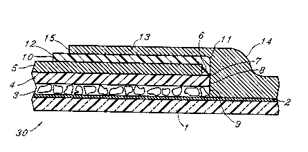
Referring now to Fig. 2 of the drawings, the electroluminescent lamp strip 30 is shown
in cross section along lines n-lI of Fig. 1. The drawing is not to scale, and the layers are
greatly enlarged for purposes of illustration, it being understood that some of the layers
referred to herein are quite thin. As a general rule, the electroluminescent lamp thickness is
only on the order of 0.15 to 0.20 mm. It may be cut and imprinted to form an analog watch
dial which is flexible and requires a support, as set forth in the aforesaid U.S. Patent No.
5,265,071. The process described herein, however, applies to an electroluminescent lamp for
any type of device, including LCD backlights for any kind of instrument.
The EL lamp strip 30 comprises a transparent substrate 1 having deposited thereon a
first conductive layer 2. Commercially, the substrate 1 with the conductive layer 2 already on
it is commercially available in the form of MylarTM (a registered trademark of E.I. duPont de
Nemours & Co.) having an indium tin oxide (ITO) coating. On the first conductive layer 2,
which may also be referred to as the front electrode, an electroluminescent layer 3 is
deposited. The electroluminescent layer 3, as is well known in the art, comprises
electroluminescent particles such as ZnS:Cu which are thoroughly mixed in a polymerizable
20 resin. The EL ~ Lure is silk screened or otherwise uniformly coated on the first conductive
2156584
19500-11479
Daigle/Ledesma/Ang
layer 2.
Next, a first insulating layer 4 is applied over the electroluminescent layer 3. This is
done by silk screening or another suitable process. The first insulating layer 4 may be
composed of barium titanate or other appropriate dielectrics. A second conductive layer S is
5 then silk screened or otherwise uniformly deposited on the first insulating layer 4. An edge 6
of the second conductive layer 5 is plefelably setback from a line 7 forrned by edges 8, 9 of
the first insul~ting layer 4 and the electroluminescent layer 3. The reason for this will
become apparent hereinafter. The second conductive layer 5, which may also be referred to
as the back electrode, may be composed of silver or any other suitable electrically conductive
o material.
Over the back electrode 5, a second in~nl~ting layer 10 is silk screened or otherwise
uniformly applied. As was the case for the first inslll~ting layer 4, the second insulating layer
10 may be comprised of barium titanate or other appropriate dielectrics. The second
in~ ting layer 10 has an insulating end 11 which extends around and encloses the edge 6 of
15 the back electrode S. Furthermore, as shown in Fig. 2, a second end 12 of the second
in~uliqting layer 10 does not extend the width of the electroluminescent lamp strip 30.
Finally, a film of conductive material 13 is applied onto the second insulating layer 10
by silk screening or other suitable process. The film 13 may be composed of silver or any
other appropriate electrically conductive material. A conductive end 14 of the film 13
20 extends around the insulating end 11 of the second in~ul~ting layer 10 and electrically
2156S84
....
19500-1 1479
Daigle/l ~des~-'Ang
contacts the front electrode 2. This permits an electrical contact area to be established on the
film 13, thereby circumventing the need to position an electrical contact area directly on the
front electrode 2. A second end 15 of the film 13, as illustrated in Fig. 2, is setback from the
second end 12 of the second insulating layer 10. Electrical separation of the back electrode 5
5 and the film of conductive material 13, which may also be referred to as the front electrode
terminal, is thus maintained since the possibility of the front electrode terminal 13 extending
over the second end 12 of the second insulating layer 10 is prevented.
Fig. 3 lepresel-ls a cross section of the electroluminescent lamp strip 30 along lines
m-m of Fig. 1. As shown in the drawing, the width of the second insulating layer 10 is
o narrower than the widths of the layers beneath it. The width of the front electrode terminal
13 is even narrower than the width of the second in~ul~ting layer 10. This ensures a
noncontacting relationship between the front electrode terminal 13 and the back electrode 5 by
precluding the possibility of the front electrode terminal 13 extending over the sides 16, 17 of
the second insulating layer 10.
A cross section of the electroluminescent lamp strip 30 along lines IV-IV of Fig. 1 is
illustrated in Fig. 4. This is similar to Fig. 2 in all respects except for the insulating end 11
of the second insulating layer 10 extending to a first edge 18 of the electroluminescent lamp
strip 30. By extending to the first edge 18, not only does the insulabng end 11 enclose the
edge 6 of the back electrode 5, but the insulating end 11 also contains the conductive end 14
20 of the front electrode terminal 13 so as to facilitate the electrical contact between the
21S6584
19500-11479
Daigle/l P~lP~ Ang
conductive end 14 and the front electrode 2 as shown in Fig. 2.
In Fig. 5, a view of the electroluminescent lamp strip 30 with the second in~ul~ting
layer 10 on top is shown. A circular dial cutout 24 is outlined as illustrated. The front
electrode terminal 13 is omitted from the drawing for purposes of clarity. Note that a shaded
region 19 behind the line 7 formed by the edges 8, 9 of the first in~nl~ting layer 4 and the
electroluminescent layer 3 represents the area where the conductive end 14 of the front
electrode terminal 13 is in electrical contact with the front electrode 2. Therefore, as long as
the dial cutout includes some portion of the shaded region 19, the object of the present
invention may be realized. Although the shaded region 19 depicted in Fig. 5 is rectangular, it
can be any shape or size desired. For instance, it can be the size of a pinhole.Fig. 6 is the same view as that shown in Fig. 5, except for a darkened region 20behind a line 25 formed by the edge 6 of the second conductive layer 5. In the preferred
embodiment, this darkened region 20 represents the area of the dial cutout where there is a
dark spot. However, because the darkened region 20 is on the edge of the dial cutout, its
presence has little effect on the luminescence of the watch dial. Furthermore, by including a
minim~l portion of the darkened region 20 in the dial cutout, the size of the dark spot present
on the dial can thus be minimi7ed. And the problems associated with the presence of a dark
spot on the dial can be virtually elimin~ted.
In another embodiment, shown in Fig. 7, the insulating end 11 of the second insulating
layer 10 is not extended to the first edge 18 of the electroluminescent lamp strip 30 as done
215658~
.
19500-1 1479
Daigle/Ledesma/Ang
in Fg. 4. Rather, the insulating end 11 termin~tes at the line 7 formed by the edges 8, 9 of
the first in~ul~ting layer 4 and the electroluminescent layer 3. Therefore, as this view of the
electroluminescent lamp strip 30 with the front electrode terminal 13 on top illustrates, the
conductive end 14 of the front electrode terminal 13 which is in electrical contact with the
5 front electrode 2 is represented by a hatched region 21. As described above, the dial cutout
need only include a portion of the hatched region 21 for the object of the present invention to
be realized. This is shown by the outline of the circular dial cutout 24.
One electrical contact terminal may be located at any desired position on the front
electrode terminal 13 included in the dial cutout. The other electrical contact terminal may be
10 located at any desired position on the back electrode 5 not covered by the second ins~ qting
layer 10. In this manner, the two terminals may be located on the back of the EL lamp
without regard to other design constraints.
While there has been described what has been considered the preferred embodiment of
the invention and a modification thereof, other modifications of the present invention will
occur to those skilled in the art, and it is desired to secure in the appended claims all such
modifications as fall within the true spirit and scope of the invention.