Note: Descriptions are shown in the official language in which they were submitted.
15G795
AN ELECTRONIC DEVICE ASSEMBLY AND
A MANUFACTURING METHOD OF THE SAME
BACKGROUND OF THE INVENTION
The present invention relates to an electronic device
assembly, and more particularly to an electronic device assembly
including a first substrate on which an electronic device is
mounted and a second substrate on which the first substrate is
mounted.
An example of a conventional electronic device is disclosed
in U.S.P. 5,203,075.
Referring to Fig. 10 of the above reference, a semiconductor
device 43 is mounted on a flexible substrate 31. The flexible
substrate 31 is connected to a substrate 13 via solder.
Referring to Figs. 6 and 9 of the reference, a solder member
32 and a solder paste 27 connects the flexible substrate 31 and
the substrate 13. Part of the solder member 32 is positioned in
a through-hole provided in the flexible substrate 31.
In a process of connecting the flexible substrate 31 and the
substrate 13, the flexible substrate 31 should be kept flat and
parallel to the substrate 13. When the flexible substrate 31
warps or deforms, the respective heights of the bumps (i.e., the
gap between a conductor 39 and a conductive pad 23 ) vary with the
positions thereof to reduce the reliability of the connection
between the flexible substrate 31 and the substrate 13.
Referring again to Fig. 10 of the above reference, the
flexible substrate 31 is stretched across frame member 47 to
maintain the flexible substrate 31 substantially parallel to the
substrate 13. The frame member 47 serves to position the
-1-
2~~s79~
flexible substrate 31 at a desired distance from the substrate
13 .
However, this conventional structure has the following
problems.
First, the conventional structure requires the frame member
47. Second, the manufacturing process of this conventional
structure requires a step of attaching the frame member to the
substrate 13 and a step of stretching the flexible substrate 31
across the frame member 47.
SUMMARY OF THE INVENTION
In view of the foregoing problems of the conventional
structure, one object of the present invention is to provide an
electronic device assembly in which a carrier substrate (e. g.,
a flexible substrate) is maintained flat without a frame member
being necessary.
Another object of the present invention is to enhance the
evenness (e. g., flatness) of a carrier substrate.
Yet another object of the present invention is to improve
the reliability of a connection between a carrier substrate and
a mounting substrate (e. g., a relatively rigid substrate).
Yet another object of the present invention is to provide
an electronic device assembly in which a connection failure can
easily be detected.
According to the present invention, an electronic device
assembly includes a rigid first substrate and a second substrate.
The first substrate has a first surface, a second surface, a
first pad on the second surface, and a through-hole at a position
of the first pad. The second substrate has a first surface, a
-2-
21 ~6~9~
second surface, and a second pad on the first surface thereof.
The first surface of the second substrate faces the second
surface of the first substrate. The first and second pads are
connected via solder. At least a part of the solder is
positioned in the through-hole of the first substrate.
The first substrate may include a ceramic sheet.
The first substrate may include a flexible substrate
and a rigid plate. The flexible substrate has a first
surface, and a second surface. The through-hole is provided
in the flexible substrate. The first pad is provided on the
second surface of the flexible substrate. The rigid plate is
attached to the flexible substrate. The plate has a hole at a
position of the through-hole.
The rigid plate may include a metal plate coated
with an insulating material.
The through-hole may be tapered.
The distance between the first and second substrates
may be adjusted by providing a core in the solder and
providing the core with a predetermined diameter.
In accordance with the present invention, there is
provided an electronic device assembly, comprising: first
substrate, said first substrate being flexible and having a
first surface, a second surface, a first pad on said second
surface, and a through-hole at a position of said first pad,
said through-hole being provided in said flexible substrate,
said first pad being provided on said second surface of said
flexible substrate; a rigid plate attached to said flexible
substrate, said plate having a hole at a position of said
3
66446-612
through-hole; a second substrate having a first surface, a
second surface, and a second pad on said first surface
thereof, said first surface of said second substrate facing
said second surface of said first substrate; and solder
connecting said first and second pads, at least a part of said
solder being positioned in said through-hole of said first
substrate.
In accordance with the present invention, there is
also provided a method for manufacturing an electronic device
assembly, comprising steps of: (a) preparing a rigid, first
substrate having a first surface, a second surface, a first
pad on said second surface, and a through-hole at a position
of said first pad; (b) preparing a second substrate having a
first surface, a second surface, and a second pad on said
first surface thereof; (c) providing solder on at least one of
said first pad and said second pad; (d) positioning said first
substrate so that said first pad faces said second pad; and
(e) heating said solder, said solder melting to connect said
first and second pads, at least a part of said solder flowing
into said through-hole)
BRIEF DESCRIPTION OF THE DRAWINGS
Other objects, features and advantages of the
present invention will become more apparent when the following
description is read in conjunction with the accompanying
drawings, wherein:
3a
66446-612
xn:
Fig. 1 shows the structure of an electronic device
assembly according to a first embodiment of the present
invention.
Figs. 2(A) to 2(C) illustrate the steps of a process
for mounting the electronic device assembly shown in Fig. 1 on
a
3b
~s
' 66446-612
2156795
substrate.
Fig. 3 shows the structure of an electronic device assembly
according to a second embodiment of the present invention.
Figs. 4 (A) to 4 (B) illustrate the steps of a process for
mounting the electronic device assembly shown in Fig. 1 on a
substrate.
Fig. 5 shows the structure of an electronic device assembly
according to a third embodiment of the present invention.
Fig. 6 shows the structure of an electronic device assembly
according to a fourth embodiment. of the present invention.
Fig. 7 shows the structure of an electronic device assembly
according to a fifth embodiment of the present invention.
Fig. 8 shows the structure of an electronic device assembly
according to a fifth embodiment of the present invention.
Figs . 9 (A) to 9 (D) illustrate the steps of a process for
mounting the electronic device assembly shown in Fig. 7 on a
substrate.
Fig. 10 shows the structure of an electronic device assembly
according to a sixth embodiment of the present invention.
Fig. 11 shows the structure of an electronic device assembly
according to a seventh embodiment of the present invention.
Fig. 12 shows the structure of an electronic device assembly
according to a eighth embodiment of the present invention.
Fig. 13 shows the structure of an electronic device assembly
according to a ninth embodiment of the present invention.
In these drawings, the same reference numerals depict the
same parts, respectively.
-4-
__ DETAILED DESCRIPTION OF T~iE PREFERRED EMBODIMENTS
Next is described a first embodiment of the present
invention.
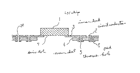
Referring to Fig. 1, an electronic device assembly according
S to a first embodiment of the present invention includes a carrier
substrate (e. g., ceramic sheet 4) and an electronic device (e. g.,
LSI chip 1) mounted on the ceramic sheet 4.
In the exemplary embodiment, the LSI chip 1 is square-shaped
having a length of approximately 17.S mm. The LSI chip 1 has 800
l0 terminals along each of the sides thereof. The terminals are
aligned with approximately an 80,m pitch.
The ceramic sheet 4 is formed from a rigid insulating
material or a composite of such materials. Specifically, the
material is preferably a borosilicate-lead-type glass ceramic.
1S The material may be other glass ceramics such as steatite-type,
forsterite-type, cordierite-type, a,nd mooreite-type ceramics.
Ceramics such as alumina-type, zirconium-type, and silica-type
ceramics can also be used.
In the exemplary embodiment, the ceramic sheet 4 is square-
20 shaped having a length of approximately 43 mm. The thickness of
the ceramic sheet 4 is about 200 Vim. Considering the flowing up
of solder described below, the thickness of the ceramic sheet 4
is set within the range of 200 ~.m to 1000 Vim. The warpage or
deformation of the ceramic sheet 4 is preferably less than 20 Vim.
25 Unlike prior ceramic substrates, ceramic sheet 4 does not
have a conductive layer therein.
The ceramic sheet 4 has a device hole 7 in the center
thereof. The device hole is square-shaped having a length of
_S_
~T<?.'Y
v
21~fi'~9~
__ approximately 18.2 mm.
A conductive pattern 2 and pad 6 are formed on the upper and
lower surfaces of the ceramic sheet 4, respectively. The
conductive pattern 2 and the pad 6 are formed from copper having
a thickness of about 10 ~.m to 20 ~.m. The pad 6 is annular and
has an outer diameter of about 400 ~.m. The pad 6 is plated with
gold having a thickness of about 1 ~.m to 5 ~.m.
The ceramic sheet 4 has a through-hole 5 having a diameter
of approximately 200 ~.m. A conductive pattern 20 is formed on
the inner surface of the through-hole 5. The conductive pattern
connects the pad 6 and the conductive pattern 2.
An inner lead 3 is provided on the upper surface of the
ceramic sheet 4. One end of the inner lead is connected to the
conductive pattern 2. Another end of the inner lead protrudes
15 above the device hole and is connected to the terminals of the
LSI chip 1. When the inner lead 3 and the LSI chip 1 are
connected, a thermode (unillustrated) is inserted in the device
hole 7.
Next is described the structure of the electronic device
20 assembly further including a mounting substrate.
Referring to Fig. 2(C), pad 12 is formed on the upper
surface of a mounting substrate 9. The pad 12 is circular-shaped
having a diameter of 600 ~.m. Solder 8 connects the pad 12 of the
mounting substrate 9 and the pad 6 of the ceramic sheet 4. Part
of the solder 8 is placed in the through-hole 5 of the ceramic
sheet 4. A portion of the solder 8 appears on the upper surface
of the ceramic sheet 4.
The mounting substrate 9 may be a glass-epoxy substrate or
-6-
215 6'~9
__ a_.ceramic substrate. The mounting substrate 9 may include a
conductive layer therein.
Next is described a process for connecting the ceramic sheet
4 to the mounting substrate 9.
Referring to Fig. 2(A), in a first step, solder 8 is
provided on the pad 12 (e. g., by a screen printing). The volume
of the solder 8 is about 3 x 10⁻¹m3. Preferable materials for the
solder 8 include tin/lead, tin/lead/antimony, tin/lead/cadmium,
and tin/lead/indium. In this exemplary embodiment, tin/lead
solder was used.
Referring to Fig. 2(B), in a second step, the ceramic sheet
4 is positioned so that the pad 6 faces the solder 8. The.LSI
chip 1 is mounted on the ceramic sheet 4 previously (in advance) .
Referring to Fig. 2 (C) , in a third step the solder 8 is
heated to a temperature in a range from about 200 °C to 250 °C
by reflowing. The solder 8 melts to connect the pads 6 and 12.
Part of the solder 8 flows into the through-hole 5 and a portion
of the solder 8 appears on the upper surface of the ceramic sheet
4. A connection failure of the solder 8 can be determined by
confirming whether a portion of the solder 8 appears on the upper
surface of the ceramic sheet 4. Specifically, if a portion of
the solder 8 appears on the upper surface of the ceramic sheet
4, the connection is normal.
In the third step, the ceramic sheet 4 is rigid and does not
warp or deform. The ceramic sheet 4 maintains a substantially
flat contour and is substantially parallel to the mounting
substrate 9. Thus, uniform gaps are provided between the pad 6
and pad 12 across the entire ceramic sheet 4.
215679
In the first step, solder may be provided on the pad 6 as
well as on the pad 12. The material of the solder on the pad 12
also may be different from that of the solder 8.
Next is described the technical advantage of the first
embodiment.
First, special attention (e.g., the frame member? and
special handling are unnecessary to maintain the ceramic sheet
flat because the ceramic sheet 4 is relatively rigid and does not
deform.
Second, connection failure can easily be detected by
confirming whether the solder 8 appears on the upper surface of
the ceramic sheet 4.
Next isdescribed a second embodiment of the present
invention
Referring to Fig. 3, the feature of the second embodiment
is the structure of the ceramic sheet 4 and the connecting
portion between the LSI chip 1 and the ceramic sheet 4. Other
structures and functions are the same as those of the first
embodiment.
The ceramic sheet 4 of the second embodiment does not have
device hole 7 nor inner lead 3. Instead, the ceramic sheet 4 has
pads 11 provided in the center of the upper surface thereof.
Other structures and the materials of the ceramic sheet 4 are the
same as those of the first embodiment.
The LSI chip 1 has terminals on the lower surface thereof.
The LSI 1 is mounted on the ceramic sheet 4 in a "face-down"
position and the terminals thereof are connected to the pads 11
via solder bumps 10.
_g_
2ms~s~
__ Next is described a process for connecting the ceramic sheet
4 to the mounting substrate 9.
Referring to Figs. 4(A) to 4(C), the ceramic sheet 4 of the
second embodiment is connected to the mounting substrate 9 by
substantially the same process shown in Figs. 2(A) to 2(C).
Next is described a third embodiment of the present
invention. The feature of the present invention is the structure
of the through-hole 5 and the other structures and functions are
the same as those of the first embodiment.
Referring to Fig. 5, the. through-hole 5 of the third
embodiment is tapered. The diameter of the through-hole 5 is
about 200 ~.m and 400 ~Cm at the upper and lower surfaces ,
respectively, of the ceramic sheet 4.
Next is described a fourth embodiment of the present
invention. The feature of the fourth embodiment is a core 21
provided between the pads 6 and 12. The other structures and
functions are the same as those of the third embodiment.
Referring to Fig. 6, a core~21 is provided between the pads
6 and 12. The melting point of the core 21 is higher than that
of the solder 8 so that the core 21 does not melt in the heating
step shown in Fig. 2(C). The core 21 is preferably formed from
a metal or a ceramic. The upper portion of the core 21 is
received in the through-hole 5. The distance between the pads
6 and 12 can be adjusted precisely due to the core 21 and
specifically by varying its diameter.
Next is described a fifth embodiment of the present
invention.
Referring to Figs. 7 and 8, an electronic device according
_g_
21~679~
__ to the fifth embodiment includes an LSI chip 101, a heat
radiating plate l08, a flexible substrate 103 on which the LSI
chip 101 is mounted, and a plate 106 attached to the lower
surface of the flexible substrate 103.
The LSI chip 101 has the same structure as that of the LSI
chip 1 of the first embodiment. The terminals of the LSI chip
101 are connected to the inner leads of the flexible substrate
103. The connecting portion between the LSI chip 101 and the
inner leads is encapsulated with a resin 102.
An adhesive 117 is applied to the upper surface of the LSI
chip 101. The adhesive 117 attaches the heat radiating plate 108
to the LSI chip 101. The adhesive 117 preferably has high heat
conductivity to effectively transfer heat from the LSI chip 101
to the heat radiating plate 108. For example, epoxy-type
adhesive including silver powder or the like can be used as the
adhesive 117.
A conductive pattern 104 is formed on the upper surface of
the flexible substrate 103. The flexible substrate 103 has
through-holes 105 having a diameter of approximately 150 ~.m. The
through-holes 105 are disposed in an array with about a 1.27 mm
pitch. A conductive pattern 120 is provided on the inner surface
of the through-hole 105. Annular pad 121 is formed on the lower
surface of the flexible substrate 103. The pad 121 surrounds the
lower opening portion of the through-hole 105. The outer
diameter of the pad 121 is about 400 ~Cm.
The conductive pattern 104 includes an annular portion
surrounding the upper opening portion of the through-hole 10S and
a linear portion connecting the inner lead and the annular
-10-
2~5679~
__ portion. The outer diameter of the annular portion of the
conductive pattern 104 is about 2S0 ~Cm. The width and thickness
of the linear portion are about 40 ~Cm and 25 ~.m, respectively.
The conductive pattern 104, the conductive pattern 120, and
S pad 121 are formed from copper plated with gold.
The flexible substrate 103 is formed from a material
preferably easily attachable to the conductive pattern l04 and
having suitable heat resistance and a relatively low thermal
expansion coefficient. In this exemplary embodiment, a polyimide
ZO film having a thickness of approximately 50 ~.m is used as the
flexible substrate 103. Other materials such as a fluorine-type
film and an epoxy-type film can also be used. .
The plate 106 serves as a stiffener to maintain the flexible
substrate 103 flat . Therefore, the plate is preferably made from
15 a rigid insulating material. In this exemplary embodiment, the
plate 106 is an alumina ceramic plate having, a thickness of about
200 ~.m. If the plate 106 has nearly the same thermal expansion
coefficient as that of the flexible substrate 103, the warpage
of the flexible substrate 103 in heating process can be reduced
20 since the thermal expansion of these materials will be
substantially the same. Polyimide and polyimide ethyl are
exemplary materials having nearly the same thermal expansion
coefficient as that of the flexible substrate 103.
The plate 106 has holes 116 at a position corresponding to
25 the through-hole 10S of the flexible substrate l03. The diameter
of the hole 116 is about 500 ~.m. The inner surface of the hole
116 may be plated with a suitable material according to the
designer's requirement.
-11-
__ The plate 106 is attached to the lower surface of the
flexible substrate 103 via an adhesive 107. The lower surface
of the flexible substrate 103 is covered with the plate 106
except for the pad 121 which is reachable through the hole 116.
The adhesive 107 preferably has suitable heat resistance,
insulation, and anti-migration properties and may be~the same
adhesive as adhesive 117. In this exemplary embodiment, an
epoxy-type adhesive is used as the adhesive 107.
Next is described a process for connecting the
aforementioned electronic device assembly and a mounting
substrate.
Referring to Fig. 9(a), in this exemplary embodiment, the
mounting substrate 109 is a glass-epoxy substrate. Pads 110 are
provided on the upper surface of the mounting substrate 109.
Each of pads 110 corresponds to one of the through-holes 105.
The pads 110 are formed from copper. The pad 110 is circular-
shaped having a diameter of 200 ~.m. ~ The upper surface of the
mounting substrate 109 is coated with a solder resist 111 except
for the pad l10.
Referring again to Fig. 9(a), in a first step, a solder
paste 112 is provided on the pad 110. The solder paste 112 may
also be provided in the area surrounding the pad 110.
Referring to Fig. 9 (b) , in a second step, a spherical solder
118 is placed on the solder paste 112. The solder paste 112 and
the solder 118 are heated to be connected together.
Specifically, the solder paste 112 and the solder 118 are heated
to a temperature in a range from about 200 °C to 250 °C for
about
seconds to 1 minute. After the connection, the height of the
-12-
__ solder 118 is.higher than the thickness of the plate 106.
Referring to Fig. 9(c), in a third step, the flexible
substrate 103 is positioned so that the pad 112 faces the
corresponding solder 118.
Referring to Fig. 9(d), in a fourth step, the solder paste
112 and the solder 118 are heated to about 200 °C to 250 °C for
about 30 second to 1 minute. In this heating, the flexible
substrate 103 may be pressed against the mounting substrate 109.
The solder paste 112 and the solder 118 melt to connect the pads
110 and 121. Part of the solder.118 flows into the through-hole
105. A portion of the solder 118 appears on the upper surface
of the flexible substrate 103.
Connection failure of the solder 118 can be determined by
confirming whether a portion of the solder 118 appears on the
upper surface of the flexible substrate 103 or not.
Specifically, if the solder appears, the connection is normal.
In the fourth step, the flexible substrate 103 is maintained
flat and parallel to the mounting substrate 109 because the
flexible substrate 103 is supported by the plate 106. Thus, the
gaps between the pads 121 and 110 become uniform across the
entire flexible substrate 103.
Next is described the technical advantage of the fifth
embodiment of the present invention.
First, special attention (e.g., the frame member) and
special handling are unnecessary to maintain the flexible
substrate 103 flat because the flexible substrate 103 is
supported by the plate 106.
Second, connection failure can easily be detected by
-13-
A
_ 21567,9
confirming whether the solder 118 appears on the upper surface
of the flexible substrate 103.
Next is described a sixth embodiment of the present
invention. The feature of the sixth embodiment is the position
of the plate l06. The other structures and func tions are
the
same as those of the fifth embodiment.
Referring to Fig. 10, in the sixth embodiment, the plate
106
is attached to the upper surface of the flexible ubstrate 103.
s
In the sixth embodiment, the height of the solder
118 is not
limited by the thickness of the plate 106.
Next is described a seventh embodiment of the present
invention. The feature of the seventh embodiment
is the
structure of the plate 106. The other structures and functions
are the same as those of the fifth embodiment.
Referring to Fig. 11, the plate 106 of the seventh
embodiment includes a metal plate 114. The metal plate 114
is
coated with an insulating material 11S such as organic
insulating
materials and/or ceramics,
Next is described an eighth embodiment of the present
invention. The feature of the eighth embodiment is the structure
of the through-hole 105. The other structures and functions
are
the same as those of the fifth embodiment.
Referring to Fig. 12, the through-hole 105 is tapered.
Specifically, the diameter of the through-hole 105 is about 200
~.m and 400 ~.m at the upper and lower surfaces of the flexible
substrate 103, respectively.
Next is described a ninth embodiment of the present
invention. The feature of the ninth embodiment is
a core 122
-14-
-- provided between the pads 110 and 121. The other structures and
functions are the same as those of the third embodiment.
Referring to Fig. l3, a core l22 is provided between the pads
110 and 121. The melting point of the core 122 is higher than
that of the solder 118 and the solder paste 112 so that the core
122 does not melt in the heating step shown in Fig. 9~d). The
core 122 is preferably formed from a metal or a ceramic. The
upper portion of the core 122 is received in the through-hole
105. The distance between the pads 110 and 121 can be adjusted
precisely due to the core 122 and suitably varying its diameter.
The present embodiments are therefore, to be considered in
all respects as illustrative and not restrictive, the scope of
the invention being indicated by the appended claims rather than
by the foregoing description and a11 changes which come within
the meanings and range of equivalency of the claims are therefore
intended to the embraced therein.
-15-