Note: Descriptions are shown in the official language in which they were submitted.
217310
-1-
METHOD AND APPARATUS FOR PROCESSING MULTICARRIER SIGNALS
Field of the Invention
The present invention relates to multicarrier signal processing and, more
particularly, to methods and apparatus which alter the dynamic range of a
multicarrier signal.
Background of the Invention
In radio transmission and reception systems, a radio receiver is typically
confronted with a multicarrier signal, i.e., a signal comprising a plurality
of carrier
signals having differing signal characteristics, such as different
frequencies. Due to
variations in broadcast strength and the different locations from which they
are
broadcast, respective carrier signals of a multicarrier signal arrive at a
particular
radio receiver have varying strengths. The difference in strength between the
highest
and lowest constituent carrier signals defines the dynamic range of the
multicarrier
signal.
FIG. 1 depicts a schematic diagram of the front-end of a conventional
radio receiver. Receiver 100 receives the broadband signal via antenna 101.
Bandpass filter 105 takes the received broadband signal and passes only the
multicarrier signal, eliminating signals whose frequencies are outside the
multicarner range defined by the filter. The multicarrier signal is mixed down
by
mixer 117 cooperating with local oscillator 125 and sent to a second bandpass
filter
119. Bandpass filter 119 selects the particular frequency band or bands of
interest
which form the output signal. Typically, the utility of a radio receiver is
limited by
the dynamic range of the receiver components that process the signals of
interest.
More specifically, the dynamic range which the radio receiver can
satisfactorily
process is usually limited, at one extreme, by noise, and at the other
extreme, by the
inherent physical characteristics of mixer 117. If the dynamic range of mixer
117 is
too low, the mixing of a multicarrier signal with a wide dynamic range can
introduce
undesirable intermodulation products into the output signal. When the radio
receiver
forms a portion of a cellular communications system, the wide variation in
signal
power levels creates particular signal processing problems. Therefore, there
is a need
in the art for signal processing elements which can process multicarrier
signals with
wide dynamic ranges without introducing distortion.in the resultant output
signal.
Such signal processors could advantageously be employed in radio receivers and
cellular communications systems to reduce the dynamic range of multicatrier
signals.
CA 02157310 1999-10-08
-2-
Summary of the Invention
The present invention provides a multicarrier signal processor capable of
reducing the dynamic range of multicarrier signals. In an exemplary
embodiment, the
multicarrier signal processor includes a controller configured to receive at
least a
portion of a multicarrier signal, the controller analyzing the signal to
identify at least
one carrier signal of the multicarrier signal to be modified. At least one
signal modifier
communicates with the controller, the signal modifier receiving at least a
portion of a
multicarrier signal. The signal modifier isolates a carrier signal to be
modified as
directed by the controller, and modifies the isolated carrier signal. A signal
combiner
receives the modified carrier signal and combines it with an unmodified
multicarrier
signal. Preferably, the multicarrier signal processor is used to reduce the
dynamic range
of a multicarrier signal.
In accordance with one aspect of the present invention there is provided
a multicarrier signal processor for processing a multicarrier signal, said
multicarrier
signal processor CHARACTERIZED BY: a controller configured to receive at least
a
portion of the multicarrier signal, the controller analyzing the at least a
portion of the
multicarrier signal to identify at least one carrier signal of the
multicarrier signal to be
modified; and at least one signal modifier, the at least one signal modifier
receiving at
least a portion of the multicarrier signal, isolating the at least one carrier
signal to be
modified as identified by the controller, and modifying the isolated at least
one carrier
signal to interact with a corresponding unmodified carrier signal.
In accordance with another aspect of the present invention there is
provided a method for processing a multicarrier signal, the method comprising:
receiving at least a portion of the multicarrier signal in a controller;
analyzing the at
least a portion of the multicarrier signal in the controller to identify at
least one carrier
signal to be modified; receiving at least a portion of the multicarrier signal
in a signal
modifier; directing the signal modifier to isolate the at least one carrier
signal identified
by the controller; modifying a characteristic of the isolated at least one
carrier signal;
and sending the modified at least one carrier signal to an output port for
combination
with the multicarrier signal.
CA 02157310 1999-10-08
-2a-
Brief Description of the Drawings
FIG. 1 depicts a schematic diagram of a conventional radio receiver
front-end.
FIG. 2 depicts an illustrative radio receiver according to the present
invention.
FIG. 3 depicts a block diagram of an illustrative embodiment of the
present invention.
FIG. 4 is a block diagram of the individual signal modifier of FIG. 3.
FIG. 5 is a block diagram of an illustrative controller as shown in
FIG. 3.
FIG. 6 is a block diagram of another illustrative controller as shown is
FIG. 3.
FIG. 7 depicts the spectral content of an exemplary multicarrier signal.
FIG. 8 depicts the spectral content of the multicarrier signal of FIG. 7
after it has been altered according to the present invention.
FIG. 9 is a schematic illustration of a cellular communications system
which incorporates the multicarrier signal processor of the present invention.
Detailed Descri tp ion
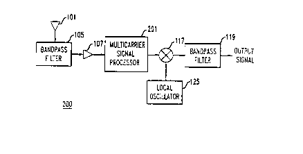
Turning now to the drawings in detail in which like numerals indicate the
same or similar elements, FIG. 2 depicts a schematic diagram of a multicarrier
signal
processor 201 according to the present invention. Illustratively, signal
processor 201 is
described as part of radio receiver front-end 200. However, it will be
appreciated by
those skilled in the art that signal processor 201 is used to process
multicarrier signals
in a wide variety of systems and devices including, but not
CA 02157310 1999-10-08
-3-
limited to radio systems, audio systems, radar systems, and the like. Radio
receiver
front-end 200 processes a multicarrier signal comprising a plurality, P, of
carner
signals, each of which is individually situated in one of a plurality, P, of
distinct
frequency bands. Any group of frequency bands can be employed, including those
frequency bands having varying widths and non-contiguous frequency bands. The
grouping of frequency bands defines a frequency range R.
FIG. 7 schematically depicts the spectral content of a typical
multicarrier signal comprising nine constituent carrier signals, labeled S1 to
S9, each
of which is situated in a distinct frequency band. The dynamic range of the
multicarrier signal is 70 dB (the difference in magnitude between the
strongest
constituent carrier signal, S3, and the weakest constituent carrier signal,
SS).
According to the present invention, the dynamic range of the multicarrier
signal in
FIG. 7 is reducible by 40 dB, as shown in FIG. 8, by attenuating the power of
signals
S 3 and S 6 by 20 dB and boosting the power of signal S 5 by 20 dB. As a
result, the
dynamic range of the processed signal of FIG. 8 is 30 dB.
Multicarrier signal processor 201 is typically employed in radio
receiver front-end 200 to reduce the dynamic range of a group of P carrier
signals of a
multicarrier signal. The radio receiver front-end generally comprises antenna
101,
bandpass filter 105, multicarrier signal processor 201, amplifier 107, mixer
117,
bandpass filter 119, and local oscillator 125. The radio receiver front-end
components
are selected from any components or group of components which perform the
stated
functions, and will not be described in detail. Further description of radio
components
such as those used in receiver front-end 100 is found in Hickman, Newnes
Practical RF
Handbook, (Newnes, Oxford), c. 1993.
Cellular communications systems employ radio receivers incorporating
radio receiver front-end 200 at several positions within a system. FIG. 9
depicts
cellular communications system 800, partitioned into a number of
geographically
distinct areas called cells. Cell 810 is schematically depicted as a hexagon,
however,
in practice a cell typically has an irregular shape depending upon the
topography of
the terrain serviced by the cellular system. Within the cell 810 is provided a
cell site
820 which generally includes a base station 822 cooperating with an antenna
824.
Radio receiver front-end 200 is typically incorporated within the base station
of cell
site 820. Wireless terminals 840 communicate with cell site 820 via radio
links. As
used herein, the expression "wireless terminals" refers to any communications
device
which receives or transmits an electromagnetic signal through the atmosphere
CA 02157310 1999-10-08
-4-
including, but not limited to, mobile telephones, pagers, and personal
communicators.
Cell site 820 optionally communicates with a mobile
telecommunications switching office (MTSO) 850, also known as a mobile
switching center (MSC). The MTSO typically comprises a large switch (e.g., the
SESS ~ switch available from AT&T Corp.) that routes call to and from wireless
terminals in the cellular system and, if necessary, to and from the public
switched
telephone network (PSTN) via a local office switch 860. Detailed descriptions
of
cellular communications systems are found in Lee, Mobile Cellular
Telecommunications S sy terns, (McGraw-Hill, N.Y.), c. 1989, Lee, Mobile
Communications Desi n Fundamentals, (Wiley-Interscience), c. 1993,
Transmission
S sy terns For Communications, (Bell Telephone Laboratories, NJ), c. 1982,
Rey, Ed.
Engineering and Operations in the Bell S_ ystem, (AT&T Bell Laboratories,
Murray
Hill, N.J.), c. 1983, and Young, Wireless Basics, (Intertec, Chicago), c.
1992.
In the frequency range of interest, R, a multicarrier signal typically
comprises a plurality of carrier signals with greatly disparate relative
powers, i.e., a
signal with a large dynamic range. Large dynamic range multicarrier signals
negatively impact the performance of numerous system components with limited
dynamic ranges such as mixers, amplifiers, and analog-to-digital converters.
For
example, when the physical dynamic range of mixer 117 is less than the dynamic
range of the multicarner signal, mixer 117 can introduce intermodulation
products
into the multicarrier signal. The intermodulation products combine with the
carrier
signals, creating a distorted output. Multicatrier signal processor 201
mitigates such
problems in an exemplary embodiment by analyzing the multicarrier signal to
determine the relative power of each of the constituent carrier signals. Based
on the
analysis, the multicarrier signal processor targets one or more of the
constituent
carrier signals whose power is beyond a particular range, the range being
preset or
determined from the multicarrier signal analysis. The multicarrier signal
processor
samples the multicarrier signal and sends at least one sampled multicarrier
signal to
a signal modifier which changes the phase and/or amplitude of the targeted
constituent carrier signal. The targeted constituent signal is selected from
an
individual frequency band or a block or frequency bands, depending upon system
needs. The modified signal is injected back into the unmodified multicarrier
signal in
a feedforward architecture. In this manner, the modified signal interacts with
the
corresponding unmodified constituent carrier signal to reduce the overall
dynamic
2157310
-5-
range of the multicarrier signal.
Multicarrier signal processor 201 reduces the dynamic range of a
multicarrier signal in an exemplary embodiment depicted in FIG. 3. FIG. 3
depicts a
block diagram of the processor 201, which comprises amplifier 390, signal
divider
301, signal combiner 303, delay 305, controller 307, and one or more
individual
signal modifiers, represented by 35N. As used herein, N represents the number
of
individual signal modifiers in a given embodiment. While there can be any
number,
N, of individual signal modifiers for a particular application, N is typically
less than
P. Furthermore, while the number of individual signal modifiers used in an
embodiment is selected based on system considerations, larger numbers of
individual signal modifiers generally increase the ability of the multicarrier
signal
processor to reduce the dynamic range of a multicanrier signal. Alternatively,
the
individual signal modifiers of the present invention can be coupled in series
such that
a multicarrier signal is sequentially processed by the individual signal
modifiers.
As depicted in FIG. 3, the incoming multicarrier signal is processed by
signal divider 301. Signal divider 301 receives the multicarrier signal and
takes N+2
samples of it, each of which is typically an analog representation of the
multicarrier
signal. Signal divider 301 places one sample of the multicarrier signal onto
each of
signal paths 311, 315, 371, ..., 37N-1 and 37N. Preferably, signal divider 301
is
fabricated so that the majority of the power of the multicarrier signal is put
onto
signal path 311. Signal divider 301 is advantageously selected from compound
splitters, which generally comprise a combination of 1:2 or 1:3 Wilkinson or
hybrid
couplers. However, any element which takes an incoming signal and provides
plural
outputs can be used as signal divider 301.
One of the sampled signals is placed on signal path 315 and fed to
controller 307. Controller 307 receives this multicarrier signal sample and
performs
several functions. First, the controller analyzes the multicarrier signal to
determine
the relative power of each of the carrier signals. This may be done on all of
the
carrier signals simultaneously (e.g., with a fast fourier transform) or
serially by
scanning for individual carrier signals, one at a time, across the frequency
range, R.
In an exemplary embodiment, controller 307 is programmed with a
threshold. The threshold is typically a range selected: such that any
constituent carrier
signal having a power below the threshold lower limit is amplified and any
constituent carrier signal having a power above upper limit is attenuated. In
this
manner, individual carrier signals with power levels that are excessively high
or
excessively low relative to the other carrier signals are automatically
attenuated or
CA 02157310 1999-10-08
-b-
automatically amplified. This threshold programming may be performed in any
known manner. In an exemplary embodiment, the multicarrier signal processor
operates with CDMA (code division multiple access) cellular communications
systems such that the CDMA equipment is not overwhelmed by signals from analog
systems. In this embodiment, the multicarrier signal comprises both CDMA
signals,
i.e., spread-spectrum-modulated signals, and higher-powered analog signals,
e.g.,
amplitude-modulated and frequency-modulated signals. Controller 307 is preset
with
an upper threshold which eliminates the substantially higher-powered analog
signals.
In this embodiment, the controller instructs the individual signal modifiers
to modify
the large carrier signal such that the modified signal, when combined with the
unmodified multicarrier signal, substantially eliminates the large carrier
signal. In a
CDMA system, the controller is typically positioned in the CDMA receiver after
the
bandpass filter, such that the mixer and other dynamic-range-sensitive
components
are not influenced by the higher-powered analog signals.
After analyzing the incoming multicarrier signal, controller 307 directs
individual signal modifiers 351,...35N-1, 35N via pathways 341...34N-1, 34N to
isolate and modify a particular constituent carrier signal from the
multicarrier signal.
Each individual signal modifier, 351...35N-1, 35N, respectively receives an
unmodified multicarrier signal sample from signal divider 301 through paths
371...37N-1, 37N. The individual signal modifier isolates its targeted
constituent
carrier signal or block of carrier signals as directed by controller 307, and
modifies
it. In an exemplary embodiment, the phase and/or amplitude of the targeted
signal
is/are changed in preparation for injection back into the unmodified
multicarrier
signal. For a constituent carrier signal having a large amplitude, the
amplitude can be
decreased by the signal modifier. Alternatively, a constituent carrier signal
can be
created having the same amplitude but 180° out of phase with the
corresponding
unmodified constituent carrier signal. For either modification technique, the
strength
of the constituent carrier signal within the multicarrier signal is reduced
upon
combination with the corresponding unmodified constituent carrier signal. The
modified constituent carrier signals are output through signal pathways 381,
38N-1,
38N to signal combiner 303 for combination with the unmodified multicarrier
signal.
Signal combiner 303 receives N+1 signals: one from signal path 311 and
one from each of the N individual signal modifiers through pathways 381...38N-
1,
38N;. and injects the modified isolated signals back into the unmodified
multicarrier
signal. Typically, combiner 303 creates an output signal that is the vector
sum of all
N+1 signals. Signal combiner 303 is generally selected from any compound
splitter,
CA 02157310 1999-10-08
_7_
particularly, compound splitters which comprise a combination of 1:2 or 1:3
Wilkinson or hybrid couplers. However, any component which combines signals
received from plural pathways can be employed as signal combiner 303.
The signal sample received from path 311 is a delayed, unmodified
multicarrier signal. Delay 305 in signal path 311 is preferably set so that
the delay
through signal path 311 is equal to the delay through signal paths 37N,
individual
signal modifiers 35N and signal paths 38N. Delay elements impart a negative
phase
slope to the signal upon which they act. Delay 305 and the phase shift
imparted by
each individual signal modifier must be carefully coordinated so that signal
combiner 303 effectively performs a vector addition of all of the signals
which enter
it. In other words, if individual signal modifier 35N is to attenuate a given
carrier
signal, delay 305 must be set so that the multicarrier signal through signal
path 311
and the isolated and modified signal through individual signal modifier 35N
arrive at
signal combiner 303 at the same time. In the case of signal attenuation, the
phase of
the output signal from the individual signal modifier is shifted 180°
relative to the
phase of the unmodified carrier signal, so that the two signals destructively
interfere.
Alternatively, delay 305 is eliminated from signal path 311 and a
negative delay element is inserted in signal paths 381, 38N-1, 38N. Negative
delay
elements, such as negative group delays, create signals which appear to have
propagated a shorter distance than the actual path length by imparting a
positive
phase slope to the signal. The use of negative delay elements in signal paths
381,
38N-1,38N, reduces the loss of the unmodified multicarrier signal in signal
path 311.
Since, in an exemplary embodiment, the majority of the signal strength
traverses
signal path 311, the overall loss in the multicarrier signal processor is
reduced
through the use of negative group delays. Exemplary negative group delays are
described in U.S. Patent 5,291,156.
For the case of carrier signal amplification, the delay 305 is identical,
since the time through the signal paths is the same. However, the phase of the
modified carrier signal from the individual signal modifier is adjusted,
relative to the
phase of the respective unmodified carrier signal, so that the two signals are
constructively added.
Individual components of multicarrier signal processor 201 will now be
described with reference to FIGS. 4-6. FIG. 4 schematically depicts an
individual
signal modifier 35N for use in the multicarrier signal processor. Each
individual
signal modifier, i.e., individual signal modifier 351, 35N-1, and 35N,
isolates a
z1~731a
_g_
targeted carrier signal and modifies its phase and/or amplitude in preparation
for
being injected back into the unmodified multicarrier signal. The individual
signal
modifier of FIG. 4 comprises mixer 401, bandpass filter 403, phase-shifter
405,
amplitude modifier 407, mixer 409, amplifier 411 and programmable synthesizer
413.
A sample of the multicarrier signal enters mixer 401 from signal path
37N. Mixer 401 mixes down the multicarrier signal, so that bandpass filter 403
can
isolate the constituent carrier signal targeted for modification by controller
307.
Programmable synthesizer 413 directs mixer 401 to shift the incoming
multicarrier
signal such that the targeted carrier signal is positioned at the pass
frequency of
bandpass filter 403. In this manner, the carrier signal targeted by controller
307 is
isolated from the multicarrier signal by bandpass filter 403. The carrier
signal that is
isolated by bandpass filter 403 will be referred to as an isolated carrier
signal.
Bandpass filter 403 is typically a high Q bandpass filter with a passband
equal to the
frequency bandwidth of the targeted signal or block of signals.
The isolated carrier signal exits the bandpass filter and is fed to phase
shifter 405. Phase-shifter 405 selectively changes the phase of the isolated
carrier
signal by a given number of degrees. For example, by shifting the phase of the
signal
' such that the signal is 180° out of phase with the unmodified carrier
signal, the
modified carrier signal destructively interferes with the unmodified carrier
signal.
When the modified signal is to constructively add with the unmodified carrier
signal,
the phase shifter is set such that the modified and unmodified carrier signals
are in
phase with one another. In this manner, the modified isolated carrier signal
from the
individual signal modifier, when injected back into the multicarrier signal by
signal
combiner 303, interacts with the corresponding unmodified carrier signal by
destructively interfering or constructively adding with the unmodified carrier
signal
to reduce the overall dynamic range of the multicarrier signal. Phase-shifter
405 is
provided with either a fixed phase shift, i.e., a phase shift preset for a
given number
of degrees, or it is provided with a variable capability that is controlled by
controller
307. In an exemplary embodiment, phase shifter 407 is programmable such that
it
adjusts the phase of the signal according to its frequency.
Following phase shifter 405, tie isolated carrier signal next enters
amplitude modifier 407. While amplitude modifier 407 is illustratively
depicted as
an attenuator, the modifier is selected from elements which can amplify,
attenuate, or
alternatively amplify or attenuate an incoming signal, e.g., amplifiers which
are
capable of both attenuating and amplifying. The amount by which signal
modifier
21~731U
-9-
407 either amplifies or attenuates the isolated carrier signal is selected to
be either
fixed or variable, depending upon system considerations. When the amount is
variable, controller 307 directs the amount of attenuation or amplification to
be
produced by amplitude modifier 407.
While each individual signal modifier can either attenuate or amplify the
isolated carrier signal, in an exemplary embodiment signals are only
attenuated.
Attenuation of signals tends to result in an overall better noise figure for
the
multicarrier signal processor. In this embodiment, amplitude modifier 407 is
selected
to be an attenuator. Typically, the attenuator attenuates the isolated ca.-
rier signal by
approximately 20 to 30 dB.
Following signal modification, the modified isolated carrier signal enters
mixer 409. Mixer 409 mixes up the modified isolated carrier signal, as
directed by
programmable synthesizer 413, to the frequency band in which the carrier
signal
resided prior to mixing down by mixer 401. The modified isolated carrier
signal is
amplified by amplifier 411, then output to signal combiner 303 via path 38N.
Following vector combination in signal combiner 303, the modified
multicarrier signal is optionally input to another multicarner signal
processor serially
connected to the previous multicarrier signal processor. This arrangement
provides
further reduction in the dynamic range of a multicarrier signal.
FIG. 5 depicts a block diagram of an illustrative embodiment of
controller 307, in which the multicarrier signal is analyzed with a fast
fourier
transform. In this embodiment, controller 307 comprises mixer 501, local
oscillator
511, bandpass filter 503, analog-to- digital converter 505, fast-fourier
transform
analyzer 507 and digital signal processor 509. The multicarrier signal
received from
signal divider 301 via signal path 315 is mixed down by mixer 501 to an
intermediate frequency, in well-known fashion. Mixer 501 is controlled by
local
oscillator 511. The mixed-down signal is input to bandpass filter 503.
Bandpass filter
503 is preferably a high Q filter with a passband width equal to the frequency
range,
R, of interest.
The filtered multicarrier signal is passed to analog-to-digital converter
505. Analog-to-digital converter 505 converts the analog output of bandpass
filter
503 to a digital format for analysis by fast-fourier transformer 507. Fast-
fourier
transformer 507 takes the multicarrier signal and produces its spectral
content, as
illustrated in FIGS. 7 and 8. Digital signal processor 509 takes the output of
fast-
fourier transformer 507, and analyzes the dynamic range, determining which
carrier
signals should be targeted for attenuation (or amplification) and, optionally,
the
CA 02157310 1999-10-08
- 10-
amount of attenuation or amplification. In one embodiment, digital signal
processor
509 also determines the amount of phase shift for each targeted carrier signal
or
block of carrier signals. Additionally, digital signal processor 509 sends a
signal to
each individual signal modifier indicating which targeted carrier signal the
individual
signal modifier is to isolate for attenuation or amplification.
FIG. 6 depicts a block diagram of an alternate embodiment of controller
307, which analyzes the multicarrier signal by scanning across it for
individual
carrier signals in sequential fashion. In this embodiment, controller 307
comprises
mixer 601, programmable synthesizer 611, bandpass filter 603, amplitude
detector
605, analog-to-digital converter 607 and digital signal processor 609. Mixer
601
mixes down the multicarrier signal from signal path 315 to an intermediate
frequency, as directed by programmable synthesizer 611. The mixed-down signal
is
sent to bandpass filter 603. Bandpass filter 603 is typically a high Q filter
with a
passband width equal to the frequency range of interest. Amplitude detector
605
takes the filtered multicarrier signal and determines the average power of the
individual scanned signal, in well-known fashion.
Analog-to-digital converter 607 converts the analog output of amplitude
detector 605 to a digital format for use by digital signal processor 609.
Digital signal
' processor 609 determines the amplitude of the carrier signal being analyzed,
and
directs programmable synthesizer 611 to serially tune to a different carrier
signal
until all of the carrier signals in the multicarrier signal have been
analyzed.
Additionally, digital signal processor 609 determines which carrier signals
should be
targeted for attenuation or amplification. The digital signal processor
directs each
individual signal modifier by sending a signal indicating which carrier signal
that
individual signal modifier is to isolate and attenuate or amplify and,
optionally, the
amount of carrier signal amplification or attenuation.
Numerous advantages are realized through the use of the multicarrier
signal processors of the present invention. For example, conventional systems
typically employ interdigital filters in the position of filter 105 which are
expensive
to produce and bulky to install at cell sites. Such filters are needed in
conjunction
with conventional receivers to prevent interference between the bands of the A
and B
carriers within a cellular market. The present invention permits the use of
smaller,
less expensive filters in the receiver since the multicarrier signal processor
essentially creates the effect of an ideal filter. Exemplary filters for use
with the
present invention are barium titanate duplex filters. Barium titanate duplex
filters are
described in U.S. Patent No. 3,938,064.
CA 02157310 1999-10-08
-11-
The present invention advantageously reduces the dynamic range of a
multicarrier signal without eliminating carrier signals and the information
which
they carry. Because individual carrier signals are merely attenuated or
amplified,
only the dynamic range is reduced without excluding the information-carrying
frequency bands of the multicarrier signal.
While the foregoing invention has been described in terms of the
exemplary embodiments, it will be readily apparent that numerous changes and
modifications can be made. Accordingly, modifications such as those suggested
above, but not limited thereto, are considered to be within the scope of the
claimed
invention.