Note: Descriptions are shown in the official language in which they were submitted.
1
ORGANIC ELECTROLUMINESCENT DEVICE AND PROCESS FOR PRODUCING
THE SAME
SPECIFICATION
The present invention relates to an organic
electroluminescent device and a process for producing t~e
same. More particularly, the present invention is
concerned with an organic electroluminescent device having
an electroluminescent layer and/or a charge
injecting/transporting layer formed out of a thin film of
organic polymers and a process for producing the same.
In data display, optical data processing and other
fields, recent attention is drawn to organic
electroluminescent materials. Any of the organic
2 0 electroluminescent materials emits light having a
wavelength and an intensity characteristic of the material
when it is sandwiched between electrodes and a voltage is
applied to the electrodes. This light emission is
generally believed to result from the injection of
2 5 electrons and holes from the respective electrodes into the
organic electroluminescent material by voltage applied to
the electrodes, followed by recombination of the holes and
electrons in the organic electroluminescent material. The
CA 02158192 1998-10-26
2
emitted light has a spectrum nearly identical with a
fluorescence spectrum intrinsic to the electroluminescent
material.
For example, Appl. Phys. Lett., Vol. 51, No. 12
(1987), pp 913-915 describes a two-layer electrolumines-
cent device (EL device) prepared with the use of organic
electroluminescent materials. This two-layer electrolumi-
nescent device is prepared by successively forming on an
electrode of ITO (indium tin oxide) a hole injecting layer,
an electroluminescent layer capable of transporting
electrons and an electron injecting electrode of MgAg alloy
according to vacuum deposition. When a voltage of tens of
Volts is applied to this electroluminescent device,
electrons and holes are injected into the
electroluminescent layer of the device to thereby emit
light. With this two-layer electroluminescent device, the
color of emitted light can be changed by choosing the type
of the electroluminescent material. For example, a low
molecular compound of an aluminum quinolinol complex (Alq3)
is used as the electroluminescent material. Green
electroluminescence is obtained by the use of the aluminum
quinolinol complex as the electroluminescent material.
However, this two-layer electroluminescent device
has a drawback in that the above low molecular
electroluminescent material forming the electroluminescent
layer is gradually crystallized to cause detachment at the
interface of the electroluminescent layer and the electrode
with the result that the electroluminescence performance is
3
deteriorated. Further, there is a case that the two-layer
electroluminescent device generates heat with the emission
of light to markedly increase the temperature of the
device, so that the device is deteriorated.
It has been proposed to form the above electron
injecting/transporting layer, electroluminescent layer or
hole injecting/transporting layer out of a thin film of a
polymer to thereby avoid the degradation and
crystallization of the layer. For example, in Japanese
Patent Laid-Open Publication No. 2096/1992, a process for
producing a polymeric thin-film electroluminescent device
is described in which a polymeric thin film comprising a
low molecular electroluminescent material or a low
molecular material capable of hole injection and electron
transport is formed by a wet process, such as spin coating
or immersion coating.
However, tens of Volts are required to be applied to
the thus obtained device for providing effective
electroluminescent brightness. This gives an
2 0 electroluminescent brightness of up to 200 cd/m2.
In the formation of the above polymeric thin film
comprising an low molecular electroluminescent material or
a low molecular material capable of hole injection and
electron transport on an electrode by spin coating, there
2 5 is a drawback such that pin holes are likely to occur in
the formed polymeric thin film, which cause the device to
break during the drive thereof.
CA 02158192 1998-10-26
4
Further, the formation of the polymeric thin film
according to the wet process has a drawback in that
impurities are likely to mingle into the device, thereby
becoming the cause of the deterioration of the device.
The polymeric thin-film electroluminescent device
comprising the polymeric thin film formed according to the
above wet process is unfavorably likely to have lowered
efficiency in electron and hole injection or likely to be
broken, although advantageously the low molecular material
contained in the polymeric thin film is less likely to
crystallize. Further, when the electroluminescent device
is produced by forming an organic layer (upper layer) on an
organic layer (sublayer) according to the wet process,
there is difficulty in selecting a solvent which does not
dissolve or leach the organic sublayer in the preparation
of a coating fluid for forming the upper organic layer.
In the formation of an organic layer (upper layer) on
an organic layer (sublayer) according to the wet process,
the materials usable for forming the sublayer and the upper
layer and the solvents for dissolving the materials are
limited. Consequently, there is a problem that the types
of the polymeric materials capable of forming the organic
layer of the polymeric thin-film electroluminescent device
and the low molecular materials which can be contained in
the polymeric materials are extremely limited.
Thus, the present applicant proposed, prior to the
filing of the present application, a method of forming
an electroluminescent layer and/or a charge
2~.~~~~ ~,
s
injecting/transporting layer of an organic
electroluminescent device according to the vapor deposition
polymerization (Japanese Patent Application 5(1993)-
103038) .
s In this method, for example, an acid chloride
represented by the following general formula:
O O
C1-C-X-C-Cl ... (XII)
wherein X represents a divalent organic group, and
a dicarbohydrazide represented by the following general
formula:
O O
a
HZNHN-C-Z-C-NHNH2 , , , (XIII)
wherein Z represents a divalent organic group, are
is subjected to a vapor deposition polymerization, thereby
forming an electroluminescent layer and/or a charge
injecting/transporting layer composed of a thin film of
polyoxadiazoles each having a repeating unit represented by
the following general formula:
N-N N-N
X -~ ~- Z -
O O
... (XI)
wherein X and Z are as defined above.
Although an organic electroluminescent device having
an organic electroluminescent layer and/or an organic
2 $ charge transporting layer having fair durability and heat
CA 02158192 1998-10-26
6
resistance are obtained by the above method, further
improvements are desired in such properties.
Moreover, in the above method, an acid (HC1) is
generated in the course of the formation of the
electroluminescent layer and/or charge
injecting/transporting layer, so that its adverse effects
on the electrodes and the device are feared. Therefore, a
process for producing an organic electroluminescent device
is desired in which an electroluminescent layer and/or a
charge injecting/transporting layer can be formed without
producing by-products of acids during the reaction.
OBJECT OF THE INVENTION
An object of the present invention is to provide an
organic electroluminescent device having an organic
electroluminescent layer and/or an organic charge
injecting/transporting layer which is excellent in
durability and heat resistance and a process for producing
the same.
A further object of the present invention is to
provide a process for producing an organic
electroluminescent device in which an electroluminescent
layer and/or a charge injecting/transporting layer can be
formed according to the vapor deposition polymerization
process without producing by-products of acids.
CA 02158192 1998-10-26
7
SUMMARY OF THE INVENTION
The present invention provides an organic thin-film
electroluminescent device comprising electrodes, at least
one of the electrodes being transparent, and, interposed
therebetween, at least one layer selected from the group
consisting of an electroluminescent layer, a charge
injection/transport layer and a layer capable of
electroluminescence and charge injection/transport, said
at least one layer formed out of a thin film of network
polymers having a network structure and obtained by the
vapor deposition polymerization process.
It is preferred that the above thin film be one
composed of polymers each having oxadiazole units
(hereinafter referred to as "thin film of
polyoxadiazoles").
A process for producing an organic electroluminescent
device (element) comprises:
providing monomer A selected from a bifunctional
monomer represented by the following formula (I) and
monomer B selected from a polyfunctional monomer
represented by the following formula (II) or a mixture of
this polyfunctional monomer and a bifunctional monomer
represented by the following formula (III):
Rl--E a ) 2 . . . ( I )
RZ-f- b ) ", . . . ( I I )
R3-f C ) 2 . . . ( I I I )
wherein:
m is an integer of 3 or greater,
CA 02158192 1998-10-26
g
each of R1 and R3 may be the same or different from
each other and independently represents a divalent organic
group,
RZ represents an m-valent organic group (provided that
m is an integer of 3 or greater),
a represents a group selected from a carboxylic acid
halide group, a carbohydrazide group and a silylated
carbohydrazide group represented by the following formula:
O-SiR3
- C = N - NH - SiR3 ...(IV)
wherein R represents an alkyl or aryl group having
not more than 6 carbon atoms,
provided that, when a is carboxylic acid halide
group, each of b and c is a carbohydrazide group or a
silylated carbohydrazide group represented by the above
formula (IV) and that, when a is a carbohydrazide group or
a silylated carbohydrazide group represented by the above
formula (IV), b and c are respective carboxylic acid
halide;
evaporating the monomers A and B from respective
separate vapor sources in vacuum so that a thin film of
polyoxadiazole precursors is formed between electrodes, at
least one of which is transparent; and
heating the thin film at 100 to 400°C in vacuum or an
inert gas, thereby converting the polyoxadiazole
precursors to polyoxadiazoles so that at least one layer
selected from the group consisting of an electrolumi-
CA 02158192 1998-10-26
9
nescent layer, a charge injection/transport layer and a
layer capable of electroluminescence and charge
injection/transport are 'formed out of the thin film of the
polyoxadiazoles.
The invention further provides a process for
producing an organic electroluminescent device comprises:
subjecting a carboxylic acid derivative represented
by the following formula:
O O
to II II
Y - C - X - C - Y ... (VIII)
wherein X represents a divalent organic group and
Y represents a halogen atom; and a silylated
dicarbohydrazide represented by the formula:
R3Si - O O - SiR3
I I
R3Si - NH - N = C - Z - C = N - NH - SiR3 . . . ( IX)
wherein Z represents a divalent organic group and R
represents an alkyl or aryl group having not more than 6
carbon atoms, to a vapor deposition polymerization on a
surface to be vapor deposited, thereby forming a thin film
of polymers each having a repeating unit represented by
the formula:
O - SiR3 O O R3Si- O
2s I II II
- C = N - N - C - X - C - N - N = C - Z -
H H ... (X)
wherein X, Z and R are as defined above; and
heating the thin film at 100 to 400°C in vacuum or an
inert gas, thereby forming at least one layer selected
CA 02158192 1998-10-26
from the group consisting of an electroluminescent layer,
a charge injection/transport layer and a layer capable of
electroluminescence and charge injection/transport
composed of (comprising) a thin film of polyoxadiazoles
5 each having a repeating unit represented by the formula:
N-N N-N
X -~ ~-- Z'_
0 O ... (XI)
wherein X and Z are as defined above.
BRIEF DESCRIPTION OF THE DRAWING
In the drawings,
10 Fig. 1 is a sectional view schematically illustrating
the structure of a first embodiment of organic thin-film
electroluminescent device of the present invention;
Fig. 2 is a sectional view schematically illustrating
the structure of a second embodiment of organic thin-film
electroluminescent device of the invention;
Fig. 3 is a sectional view schematically illustrating
the structure of a third embodiment of organic thin-film
electroluminescent device of the invention;
Fig. 4 is a sectional view schematically illustrating
the structure of a fourth embodiment of organic thin-film
electroluminescent device of the invention; and
Fig. 5 is a view illustrating the processes for
producing an organic thin-film electroluminescent device.
CA 02158192 1998-10-26
11
DETAILED DESCRIPTION OF THE INVENTION
The organic electroluminescent device of the present
invention and the process of the present invention for
producing the same will be described in detail below with
reference to the drawings.
Organic Electroluminescent Device
Figs. 1 to 4 illustrate the first to fourth
embodiments of organic electroluminescent devices of the
present invention, respectively.
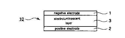
The first embodiment of organic electroluminescent
device 10 of the present invention as illustrated in Fig.
1 has a laminate structure composed of a negative
electrode 1 / an electroluminescent layer 3 / a positive
electrode 2.
The second embodiment of organic electroluminescent
device 10 of the invention as illustrated in Fig. 2 has a
laminate structure composed of a negative electrode 1 / an
electron injection/transport layer 4 / an electro-
luminescent layer 3 / a positive electrode 2.
The third embodiment of organic electroluminescent
device 10 of the invention as illustrated in Fig. 3 has a
laminate structure composed of a negative electrode 1 / an
electroluminescent layer 3 / a hole injection/transport
layer 5 / a positive electrode 2.
The fourth embodiment of organic electroluminescent
device 10 of the invention as illustrated in Fig. 4 has a
laminate structure composed of a negative electrode 1 / an
electron injection/transport layer 4 / an electro-
CA 02158192 1998-10-26
12
luminescent layer 3 / a hole injection/transport layer 5 /
a positive electrode 2.
In the first to fourth forms of organic electrolumi-
neacent devices of the invention as illustrated in Figs. 1
to 4, without exception, an electrode formed out of Mg,
Ag, In, Ca, A1 or the like is used as the negative elec-
trode 1 (electron injecting electrode) and an electrode
formed out of ITO (indium tin oxide), Au or the like as
the positive electrode 2 (hole injecting electrode).
At least one of the negative electrode 1 and the
positive electrode 2 is transparent, through which
irradiation of light can be emitted to the electro-
luminescent layer 3.
Generally, either the negative electrode 1 or the
positive electrode 2 is formed on a transparent plate of
glass, a polymer film or the like. For example, when the
positive electrode 2 is composed of ITO, the ITO electrode
is formed in the form of a thin film on a transparent
plate of glass, a polymer film or the like.
In the first embodiment of organic electroluminescent
device 10 of the invention, the electroluminescent layer 3
illustrated in Fig. 1 is composed of a thin film of
network polymers.
In the second embodiment of organic electrolumines-
cent device 10 of the invention, at least one or
preferably both of the electron injecting/transporting
layer 4 and the electroluminescent layer 3 illustrated in
Fig. 2 are composed of a thin film of network polymers.
CA 02158192 1998-10-26
13
In the third embodiment of organic electroluminescent
device 10 of the invention, at least one or preferably
both of the electroluminescent layer 3 and the hole
injecting/transporting layer 5 illustrated in Fig. 3 are
composed of a thin film of network polymers.
In the fourth embodiment of organic electrolumines-
cent device 10 of the invention, at least one or
preferably all of the electron injecting/transporting
layer 4, the electroluminescent layer 3 and the hole
injecting/transporting layer 5 illustrated in Fig. 4 are
composed of a thin film of network polymers.
In the formation of the electroluminescent layer 3
out of a thin film of network polymers of the invention,
it is preferred that the thin film is that obtained by the
vapor deposition polymerization process and that its
thickness range is from 100 to 2000 A, especially from 300
to 1000 A.
In the formation of the electron injecting/-
transporting layer 4 or the hole injecting/transporting
layer 5 out of a thin film of network polymers of the
invention, it is preferred that the thin film is that
obtained by the vapor deposition polymerization process
and that its thickness range is from 100 to 5000 A,
especially from 300 to 1000
The above thin film of network polymers is obtained
by the polycondensation or polyaddition of a polyfunction-
al monomer including an m-functional monomer (m is an
integer of at least 3) according to the vapor deposition
~~~8~~~
14
polymerization process. In particular, it is formed by the
mutual bonding of at least one polymer unit selected from
among oxadiazole unit, imide bond, amide bond, amide-imide
bond, urea bond and azomethine bond.
Among the polymer units, the oxadiazole unit has self-
electroluminescent properties, so that it is preferred that
the thin film of network polymers comprise oxadiazole
units. That is, when the thin film of network polymers is
formed out of polymers having oxadiazole units, it exhibits
excellent electroluminescence.
Especially, detailed description will be made below
with respect to the polyoxadiazole having network
structure.
In the above polyoxadiazole of network structure, the
divalent organic group R1 and the m-valent organic group R2
(m is an integer of 3 or greater) are bonded together via
the divalent oxadiazole represented by the following
formula:
N-N
to thereby form a network. It is not necessary for all the
R1 groups to be individually bonded with the R2 group via
the above divalent oxadiazole. Part of the R1 groups may
be individually bonded with the R3 group via the above
2 5 divalent oxadiazole.
It is preferred that the value of [R3 / (R2 + R3)]
100 range from 0 to 90 molo.
21~~~~~
With respect to the above polyoxadiazole of network
structure, the oxadiazole ring has self-electroluminescent
properties, so that there is no limitation except that R1
and R3 are divalent organic groups and R2 is an m-valent
5 organic group (m is an integer of 3 or greater). However,
when the electron injecting/transporting layer 4 or the
hole injecting/transporting layer 5 is formed out of the
polyoxadiazole of network structure, it is preferred that
the polyoxadiazole be produced from the starting materials
10 described later.
It is preferred that R1 and R2 be organic groups
having respective aromatic rings. When at least one of R1
and R2 is an organic group having an aromatic ring, i.e., a
divalent organic group composed mainly of a unit capable of
15 n-electron conjugation so as to enable electron
delocalization such as a phenylene group, a biphenylene
group or a divalent organic group derived from a
triphenylamine, the electron injecting/transporting layer 4
can possess improved ability of electron transporting and
2 0 the hole injecting/transporting layer 5 improved ability of
hole transporting.
When it is desired to enhance the ability of electron
transporting in the electron injecting/transporting layer
4, an additive for promoting electron injection and
2 S transport, such as diphenoquinone and fluorenone
derivatives disclosed in Chem. Mater., Vol. 3 (1991) pp.
709-714 and J. Imag. Sci., Vol. 29, No. 2 (1985) pp. 69-72,
may be added in an amount of generally from 0.01 to 80
CA 02158192 1998-10-26
16
mol%, preferably from 1 to 60 mol% per oxadiazole unit of
the above polyoxadiazole. Also, when it is desired to
enhance the ability of hole transport in the hole
injecting/transporting layer 5, an additive for promoting
hole injection and transport, such as 4,4',4 " -tris(N,N-
diphenylamino)triphenylamine, 4,4',4 " -tris[N-(3-
methylphenyl)-N-phenylamino]triphenylamine and other
triphenylamine derivatives disclosed in Chem. Lett., 1989,
p. 1145, may be added in an amount of generally from 0.01
to 80 mol%, preferably from 1 to 50 mo1% per oxadiazole
unit of the above polyoxadiazole. As apparent from the
above, the organic electroluminescent device of the
invention can be modified in various ways as long as such
modification falls within the scope of the claims.
In each of the above organic electroluminescent
devices 10 illustrated in Figs. 1 to 4, a protective film,
such as an antioxidant film, may be provided so as to
cover the surface of the portion thereof where a negative
electrode 1 or a positive electrode 2 is formed.
Alternatively, the whole of the organic electroluminescent
device 10 may be sealed with the above protective film.
The formation of the protective film on the negative
electrode 1 or positive electrode 2 increases the
stability of the negative electrode 1 or the positive
electrode 2, thereby improving the practicability and
durability of the organic electroluminescent device 10.
This protective film may be composed of a metal exhibiting
a high work function, an epoxy resin, a silicone resin or
a fluorinated resin.
2~.~8~
m
~rnrPSS for Producing Organic Electroluminescent Device
The above thin-film electroluminescent device having
an electroluminescent layer and/or a charge
S injecting/transporting layer formed out of a polymeric thin
film obtained by polycondensation or polyaddition of a
polyfunctional monomer can be produced through the steps
of
(1) forming an electrode 1 or 2 on a plate;
(2) optionally forming a first charge
injecting/transporting layer 4 or 5 on the electrode 1 or 2
according to the vapor deposition polymerization process;
(3) forming an electroluminescent layer 3 on either
the electrode 1 or 2 or the first charge
injecting/transporting layer 4 or 5 according to the vapor
deposition polymerization process;
(4) optionally forming a second charge
injecting/transporting layer 4 or 5 capable of transporting
charges opposite to those transported by the first charge
2 0 injecting/transporting layer 4 or 5 (for example, the
second charge transporting layer is a hole transporting
layer 5 when the first charge transporting layer is an
electron transporting layer 4) on the electroluminescent
layer 3 according to the vapor deposition polymerization
2 5 process;
(5) forming a counter electrode 1 or 2 [when the
electrode formed (for example, in step 1) is a negative
electrode 1, the counter electrode is a positive electrode
1g
2] on either the electroluminescent layer 3 or the second
charge transporting layer 4 or 5; and
(6) optionally forming a sealing layer for
electroluminescent element on the counter electrode.
In particular, the electroluminescent layer or charge
injecting/transporting layer composed of a thin film of
polyoxadiazoles can be formed by the process comprising:
providing monomer A consisting of a bifunctional
monomer represented by the following formula (I) and
1~ monomer B consisting of a polyfunctional monomer
represented by the following formula (II) and/or a
bifunctional monomer represented by the following formula
(III)
Rl~a )2 ... (I)
R2-~ b )rr, ... (II)
1 5 R~ ~ )2 ...(III)
evaporating the monomers A and B from respective
separate vapor sources in vacuum so that a thin film of
polyoxadiazole precursors is formed between electrodes, at
2 0 least one of which is transparent; and
heating the thin film at 100 to 400°C, preferably 100
to 350°C and still preferably 200 to 300°C in vacuum or an
inert gas for preferably 10 to 240 min, still preferably 60
to 120 min, thereby converting the polyoxadiazole
2 5 precursors to polyoxadiazoles.
In the above formulae (I) to (III),
CA 02158192 1998-10-26
19
m is an integer of 3 or greater,
each of R1 and R3 independently represents a divalent
organic group, Ra represents an m-valent organic group
(provided that m is an integer of 3 or greater),
S a represents a group selected from a carboxylic acid
halide group, a carbohydrazide group and a silylated
carbohydrazide group represented by the following formula:
O-SiR3
- C = N - NH - SiR3 . . . ( IV)
wherein R represents an alkyl or aryl group having
not more than 6 carbon atoms,
provided that, when a is a carboxylic acid halide
group, each of b and c is a carbohydrazide group or a
silylated carbohydrazide group represented by the above
formula (IV) and that, when a is a carbohydrazide group or
a silylated carbohydrazide group represented by the above
formula (IV), b and c are respective carboxylic acid
halide.
In either case, b and c may be identical with or
different from each other.
In the first process for producing an organic
electroluminescent device, a polyfunctional monomer
represented by the above formula (II) or a mixture of this
polyfunctional monomer and a bifunctional monomer
represented by the above formula (III) is used as monomer
B to thereby form an electroluminescent layer and/or a
charge injecting/transporting layer out of a
2~~~~
thin film of polyoxadiazoles of network structure having
excellent heat resistance and durability.
Examples of the above bifunctional monomers
represented by the above formula (I), polyfunctional
5 monomers represented by the above formula (II) and
bifunctional monomers represented by the above formula
(III) include monomers represented by the following
formulae (V), (VI) and (VII), respectively.
O
1
R ( -C - C1)1 ... (V):
O
0
R' ( - C - NHNH2)m ... (VI):
O - Si (Me)3
R"(-C =N-NH-Si(Me)3)n .(VII)
In the above formulae, R, R' and R" represent
valent, m-valent and n-valent organic groups, respectively.
When 1 = 2, m and/or n is an integer of 3 or greater.
When 1 is an integer of 3 or greater, m or n is 2.
When 1 is 2 while m is an integer of 3 or greater, or
when 1 is an integer of 3 or greater while m is 2, an
electroluminescent layer and/or a charge
injecting/transporting layer is formed out of a thin film
2 0 of polyoxadiazoles of network structure through the step of
reacting the monomer represented by the above formula (V)
with the monomer represented by the above formula (VI).
Likewise, when 1 is 2 while n is an integer of 3 or
greater, or when 1 is an integer of 3 or greater while n is
21
2, an electroluminescent layer and/or a charge
injecting/transporting layer is formed out of a thin film
of polyoxadiazoles of network structure through the step of
reacting the monomer represented by the above formula (V)
with the monomer represented by the above formula (VII).
In the production of an organic electroluminescent
device having the electroluminescent layer and/or a charge
injecting/transporting layer formed out of a thin film of
polyoxadiazoles of network structure in the above manner,
the molar ratio of the monomer represented by the above
formula (V) to the monomer represented by the above formula
(VI) ((V) . (VII) and the molar ratio of the monomer
represented by the above formula (V) to the monomer
represented by the above formula (VII) ((V) . (VII)) during
the polymerization are preferred to be regulated to m . 1
and n . 1, respectively, for attaining stoichiometric
reaction between the monomers.
In the above manner, an organic electroluminescent
device having an electroluminescent layer and/or a charge
2 0 injecting/transporting layer formed out of a thin film of
polyoxadiazoles of network structure is produced through
the step of reacting a bifunctional monomer (e. g., monomer
represented by the above formula (V) when 1 = 2) with a
polyfunctional monomer of 3 or higher in functionality
2 S (e.g., monomer represented by the above formula (VI) when m
is an integer of 3 or greater). The above polyfunctional
monomer includes a mixture of this polyfunctional monomer
22
and a bifunctional monomer, in which the content of the
bifunctional monomer preferably ranges from 0 to 90 molo.
In the formation of a charge injecting/transporting
layer of an organic electroluminescent device out of a thin
S film of polyoxadiazoles, it is preferred that at least one
member of the compounds represented by the above formula
1~
(I) to (III) be selected from the following compound group
(A) and compounds obtained by combining them by means of a
bonding group.
R4 R11 R4 R12 R13 R4
R9 / R5 R10 / \ R5 R11 / \ \ R5
R8 \ ~ R6 R9 \ ( / R6 R1 \ ( / / R6
R7 RS R7 R9 RS R7
R12 13 R4 R5 R14 15 16 R17 R4 R5
Rll ~ ~ ~ ~ R6 R13 \ ~ ~ ~ ~ ~ Rs
R10 R9 R8 R7 R12 Rll R10 R9 RS R7
R4 R4
Rs Nw R4 R7~N R4 R7 w N
R7
R7 ~ / R5 N w ~ R5 ~ ~ N R6 i N
R6 R6 R6 N ~ R5 R5
R6 R7 RS R9
R6 'N ~ R4 _ _
YIN /N R5 ~ ~ ~ R1o
N N
R5 R4 R11
R11 R4 R11 R4
N- -N -N -N
R1o ~ ~ ~ ~ R5 R1o ~ ~ ~ I R
1 5 R9 RS R7 R6 R9 RS R7 R6
23
Rq 9. 4
N
6 5 6 S 5 9 5' \ S /N
R 0 R R S R R S R R
Rs ° Ra R~ R4
R5 R4 9
° o
\ R~ ~ ~R5
~ SiN Rs SiN Rs Rs - R5
TTI~ wt
7
R R8 R~ R' R4
N~ R4 R9 / ~ R6
N
6~N ~ iN \ ~ / 5 R~ R5
R Ri o ~ ~' R
Rs Rll ° R9 NL my
When a compound selected from the above exemplary
compound group (A) is employed as the compound represented
by the above formula (I) or (III), two of the R4 to R1~
substituents of the compounds in the above exemplary
compound group (A) are each independently reactive
substituent selected from carboxylic acid halide groups
such as carboxylic acid chloride groups, carbohydrazide
groups and the silylated carbohydrazide groups represented
by the above formula (IV). when an m-valent compound
1$ selected from the above exemplary compound group is
employed as the compound represented by the above formula
(II), the m substituents of the R4 to R1~ substituents of
the compounds in the above exemplary compound group (A) are
each independently reactive substituent selected from
2 0 carboxylic acid halide groups, carbohydrazide groups and
24
the silylated carbohydrazide groups represented by the
above formula (IV).
Each of the other substituents of the compounds in the
above exemplary compound group (A) is independently a group
selected from the group consisting of a hydrogen atom, a
halogen atom, a cyano group, a nitro group, an alkyl group,
an aralkyl group and an alkyloxy group.
When the compounds represented by the above formulae
(I) to (III) are those obtained by bonding compounds in the
above exemplary compound group (A) by means of a bonding
group, at least one member of the above other substituents
is a direct bond or a bonding group such as -CH2-, -SiH2-,
-O-, -S-, -C (CHg) 2-, -CH (CH3) -, -CH (Ph) - or -Si (CH3) 2-.
Via this direct bond or bonding group, a plurality of
1$ compounds are bonded together. The plurality of compounds
may be identical with or different from each other and are
selected from the above exemplary compound group (A).
In the formation of a hole injecting/transporting
layer of an organic electroluminescent device out of a thin
2 0 film of polyoxadiazoles, it is preferred that at least one
member of the compounds represented by the above formula
(I) to (III) be selected from the following compound group
(B) and compounds obtained by combining them by means of a
bonding group.
25
R19 R28 R29
R1a
R18 R2o ~ 19
/ ~ R27 ~ ~ / ~ R
\ ~ R2o
N N / ~ N R21
R26 ~ ~ ~ 21 R26
R ~ ~ / R22
R25 . R24 R23 R22 R25 R24 R23
R1a
R19
/ R22 R23
Et ~ ~ ~ w R2o Rla 19
R
Et ~ N N \ R2i R21 ~ / /
Rzo
/ R22 N ~ ~ N
R23 Et/ \ Et
R29 R19 R19
R2a R3o R1$ R2o Ris R2o
\ ( ~ / ( \
Et /
N N \ R21 N N R21
R27 ~ \ ~ / ~ \
/ R22 Et ~ / ~ / R22
R26 R25 R24 R23 R24 R23
R2a R29
Ris
R19
R27 \ / R3o R3i /
N /I\ ~ N w R2o
R21
R26 w ~ \
R22
R25 R24 R23
2~~~~~
26
R1g R18
R20 \ ~ R29 R25
N /I\ ~ N~Et
R21 ' ~ ~ \ Et
R22 R23
R22 R23 18
- R
Rls
R21 \ ~ R29 R25
- ~ R2o
~N ~ ~ N\
Et Et
R2s R2s
R27 \ / R3o
N /~~ R31
Rla
R2 6 ~ ~ .
R1s
R25 N \
R24 R20
R21
R23 R22
R28 R2s R18 Rls
R27 ~ ~ ~ ~ R2o
N ~ / C = N-N
_ H
R26 \ ~ ~ ~ R21
R25 R24 R23 R22
2~~8~ ~~
27
R25 R26
R24
Rla
N / \ C=C ~ / R19
R23 ~ H H
R2o
R22 . R21
' R28 R29 R18 R19
R2~ ~ ~ ~ ~ R2o
R23 R22 21
N ~ / C=N-N R24 R
_ H ~ '-
R26 ~ ~ ~ ~ R21 R25 ~ ~ \ ~ R20
R25 R24 R23 R22 R26 R18 R19
$ When a compound selected from the above exemplary
compound group (B) is employed as the compound represented
by the above formula (I) or (III), two of the R18 to R31
substituents of the compounds in the above exemplary
compound group (B) are each independently reactive
substitudent selected from carboxylic acid halide groups,
carbohydrazide groups and the silylated carbohydrazide
groups represented by the above formula (IV). When an m-
valent compound selected from the above exemplary compound
group (B) is employed as the compound represented by the
1$ above formula (II), the m substituents of the R1a to R31
substituents of the compounds of the above exemplary
compound group (B) are each independently reactive
substituent selected from carboxylic acid halide groups,
28
carbohydrazide groups and the silylated carbohydrazide
groups represented by the above formula (IV).
Each of the other substituents of the compounds of the
above exemplary compound group (B) is independently a group
selected from the group consisting of a hydrogen atom, a
halogen atom, a cyano group, a nitro group, an alkyl group,
an aralkyl group and an alkyloxy group.
When the compounds represented by the above formulae
(I) to (III) are those obtained by bonding compounds of the
1~ above exemplary compound group (B) by means of a bonding
group, at least one member of the above other substituents
is a direct bond or a bonding group such as -CH2-, -SiH2-,
-O-, -S-, -C (CH3) 2-, -CH (CH3) -, -CH (Ph) - or -Si (CH3) 2-
Via this direct bond or bonding group, a plurality of
compounds are bonded together.
The plurality of compounds may be identical with or
different from each other. In the formation of an
electroluminescent layer of an organic electroluminescent
device out of a thin film of polyoxadiazoles, there is no
2 0 particular limitation except that R1 of the above formula
(I) and R2 of the above formula (II) are respective
divalent organic groups and that R3 of the above formula
(III) is a divalent organic group, because the
polyoxadiazoles themselves have fluorescence self-emitting
2 5 capability. However, when compounds of the above exemplary
compound group (B) or those obtained by bonding them are
used as the compounds represented by the above formulae (I)
to (III), advantageously not only electroluminescent
~1 ~~~ '~~'
29
capability but also capability of charge injection and
transportation are imparted to the thin film of
polyoxadiazoles as the electroluminescent layer.
Further enhanced electroluminescent intensity can be
realized by the use of residues derived from dyes for laser
selected from the following compound group (C) as the above
R1 and R3.
R32
R33
AT/~ /~7T
R35 R R31
\N v
N
R3q R32
R33 R30
R32 i N N ~ R31 R30 R31
R32
R3\N / ~ 0
1 O R3q R33
R35 t B O ~ ~ ~ ~ 0 R3o
31
R3q N / \ / \ N \ / R
R33 0 0 R32
t-Bu
When a compound selected from the above exemplary
compound group (C) is employed as the compound represented
1 5 by the above formula ( I ) or ( I I I ) , two of the R3~ to R35
substituents of the compounds in the above exemplary
CA 02158192 1998-10-26
compound group (C) are each independently reactive
substituent selected from the carboxylic acid halide
groups, carbohydrazide groups and the silylated
carbohydrazide groups represented by the above formula
S (IV). When an m-valent compound selected from the above
exemplary compound group (C) is employed as the compound
represented by the above formula (II), the m substituents
of the R3° to R35 substituents of the compounds of the above
exemplary compound group (C) are each independently
10 reactive substituent selected from carboxylic acid halide
groups, carbohydrazide groups and the silylated
carbohydrazide groups represented by the above formula
(IV) .
Each of the other substituents of the compounds of
15 the above exemplary compound group is independently a
group selected from the group consisting of a hydrogen
atom, a halogen atom, a cyano group, a nitro group, an
alkyl group, an aralkyl group and an alkyloxy group.
An electroluminescent layer formed out of a thin film
20 of polymers each having any of the above bonding units
derived from fluorescent dyes or pigments and the
oxadiazole unit emits fluorescence characteristic of the
relevant fluorescent dye or pigment at the time of
electroluminescence. For example, an electroluminescent
25 device having an electroluminescent layer formed out of a
thin film of polymers each having any of the above bonding
units derived from fluorescent dyes or pigments, such as
coumarin 343, aluminum quinolinol complex, NK 757 and DCM,
CA 02158192 1998-10-26
31
and the oxadiazole unit emits bluish-green, green, yellow
or red light depending on the type of relevant fluorescent
dye or pigment.
Now, the second process for producing an organic
electroluminescent device will be described in greater
detail.
The second process for producing an organic
electroluminescent device comprises:
subjecting a carboxylic acid derivative represented
by the following formula:
O O
Y - C - X - C - Y . . . (VIII)
wherein X represents a divalent organic group and
Y represents a halogen atom; and a silylated
dicarbohydrazide represented by the formula:
R3S1 - O O - SiR3
R3Si - NH - N = C - Z - C = N - NH - SiR3 . . . ( IX)
wherein Z represents a divalent organic group and R
represents an alkyl or aryl group having not more than 6
carbon atoms, to a vapor deposition polymerization on a
surface to be vapor deposited, thereby forming a thin film
of polymers each having a repeating unit represented by
the formula
O - SiR3 O O R3Si- O
- C = N - N - C - X - C - N - N = C - Z -
H H . . . (X)
wherein X, Z and R are as defined above; and
CA 02158192 1998-10-26
32
heating the thin film at 100 to 400°C, preferably 100
to 350°C, in vacuum or an inert gas, thereby forming an
electroluminescent layer and/or a charge
injecting/transporting layer composed of a thin film of
polyoxadiazoles each having a repeating unit represented
by the formula:
%_1 l_1
... (XI)
0 0
wherein X and Z are as defined above.
The above process for producing an organic
electroluminescent device is substantially similar to the
first process for producing an organic electroluminescent
device, except that the carboxylic acid derivative
represented by the above formula (VIII) is employed as
monomer A (or monomer B) and the silylated
dicarbohydrazide represented by the above formula (IX) as
monomer B (or monomer A). Further, the carboxylic acid
derivative represented by the above formula (VIII)
corresponds to the compound represented by the above
formula (I) which was employed in the first process for
producing an organic electroluminescent device, and the
silylated dicarbohydrazide represented by the above
formula (IX) is regarded to be included in the compound
represented by the above formula (I).
CA 02158192 1998-10-26
33
The vapor deposition polymerization on a surface of
the carboxylic acid derivative represented by the above
formula (VIII) and the silylated dicarbohydrazide
represented by the above formula (IX) forms a thin film of
polymers each having a repeating unit represented by the
following general formula:
O - SiR3 O O R3Si- O
- C = N - N - C - X - C - N - N = C - Z -
H H . . . (X)
wherein X, Z and R are as defined above.
In this vapor deposition polymerization, it is
important to accurately control the rate of evaporation of
each of the above two types of monomers so as to effect
stoichiometric control of the amount of each monomer
evaporated.
However, when a monomer is present which evaporates
at room temperature prior to reaching a predetermined
degree of vacuum, it is difficult to accurately control
the rate of evaporation of the monomer. Therefore, it is
preferred that the monomer for use in the vapor deposition
polymerization be selected from among the compounds which
scarcely evaporate at room temperature or below before
reaching a predetermined degree of vacuum.
In the second process, the above two types of
monomers are generally evaporated at a rate of at least
10-10 mol/cmZ.sec under a pressure of 10-a to 10-4 Pa,
CA 02158192 1998-10-26
34
preferably 10-3 to 10'4 Pa and polymerized on a surface to
be vapor deposited.
Therefore, it is desired that the above two types of
monomers can be individually evaporated at a rate of at
least 10-1° to 10-5 mol/cmZ.sec at 40 to 400°C, preferably 70
to 300°C and still preferably 100 to 250°C under a
pressure within the above range.
From the above viewpoint, it is preferred that the
silylated dicarbohydrazide represented by the above
formula (IX) have as its R a group selected from the group
consisting of methyl, ethyl, n-propyl, isopropyl, n-butyl,
isobutyl, sec-butyl, pentyl and phenyl groups.
For example, when Y of the above formula (VIII)
represents a chlorine atom and R of the above formula (IX)
represents a methyl group, the carboxylic acid derivative
represented by the above formula (VIII) reacts during the
vapor deposition polymerization with the terminal of
trimethylsilylated dicarbohydrazide represented by the
above formula (IX), -Si(CH3)3, to thereby form chloro
trimethylsilane of the formula ClSi(CH3)3 by by-product.
It is less probable for this by-product to corrode the
electrode of the organic electroluminescent device or the
body of the vapor deposition apparatus as different from
the above inorganic acid.
In the second process, the thin film of polymers each
having the repeating unit represented by the above formula
(X) is then heated at 100 to 400°C in vacuum or an inert
gas stream, thereby forming an electroluminescent
35
layer and/or a charge injecting/transporting layer composed
of a thin film of polyoxadiazoles each having a repeating
unit represented by the formula:
N-N N-N
~' X ~ ~- Z -
S . ~ ~ ... (XI)
wherein each of X and Z independently represents a
divalent organic group.
It is preferred that the thickness of each of the thus
formed layers range from 200 to 2000 A from the viewpoint
that an organic electroluminescent device which is
excellent in electroluminescent efficiency, heat resistance
and durability can be obtained.
The polyoxadiazole of the thin film represented by the
above formula (XI) comprises oxadiazole rings as polymer
units, and the oxadiazole rings per se have
electroluminescent properties. However, if X and/or Z of
the above formula (XI) has electroluminescent and charge
injecting/transporting properties, the electroluminescent
2 0 efficiency of the organic electroluminescent device can be
further improved. From this viewpoint, it is preferred
that the above X and/or Z be a group having
electroluminescent and/or charge injecting/transporting
properties.
2 5 With respect to the above organic groups X and Z, the
organic group X is a group derived from the carboxylic acid
derivative represented by the above formula (VIII) and the
CA 02158192 1998-10-26
36
organic group Z a group derived from the dicarbohydrazide
represented by the above formula (IX). That is, all the
organic groups X of the above formulae (VIII), (X) and
(XI) are identical groups and all the organic groups Z of
the above formulae (IX), (X) and (XI) are identical
groups.
The above organic groups X and Z may be identical
with or different from each other. For producing an
organic electroluminescent device having high
electroluminescent efficiency, it is preferred that each
thereof represent a divalent organic group composed mainly
of a unit capable of conjugating with n electrons so as to
be capable of delocalizing charges, especially a vinylene
group, a phenylene group, a biphenylene group or a
divalent group derived from triphenylamine. When each of
the above organic groups X and Z is selected from among a
vinylene group, a phenylene group, a biphenylene group and
a divalent group derived from triphenylamine, these may be
substituted with a group selected from the group
consisting of alkyl, allyl, aryl and aralkyl groups.
In the production of an organic electroluminescent
device having a charge injecting/transporting layer formed
out of a thin film of polyoxadiazoles with high capability
of electron charge and transport in conformity with the
second process for producing an organic electroluminescent
device, it is preferred that the organic groups X and Z be
respective groups selected from among the following
substituent group (1) or groups obtained by
37
combining them. These groups can be formed from the
compounds of the above compound group (A).
~ ~ ~ t-Bu
i ~ i ~ i t-Bu ~ i
R R
t-Bu
N
~N I N R1 ~N I
/ . /
I 1 Rl ~ 1 I 1
N ~N / N N
J ~ , J Rl ~ ~ 1 ~N
R
R1 R1 R1 N
\~ ~N
w w 1 ~ I ~N
~N 1 f N R i
R ~ ~ R ~ ~ i N R ~, 'I I
N N ~ ' vN
R2
w N ~N ~ ~~ I \ R2 / I \ R3
i ~ I N ~ \ ~ \ /
R
N R1 R3
R3
R2 / \ \ R3 2 / (\ \
\ I / /~ R
\ / /
R3
~\ \
RZ- ( I R4
\ / /
R2 R3 R9
~1~~~
38
\ / \ \ / \ \ / \ /
R2 R3 R2 R3 R2 R3
~N N\ ~N N\ ~N/ N\
R2 _ R3 RZ R3 R2 R3
N- -N N-
\/ ~ v _ ~ -~ / \
N N
R2 ~R3 R2 R3 R2 R3
R2~N- -N N /Rz R3
\ / \\
\ / \ /
R3
-N -N
\ / \ / / / \ \
R2 R3 R2 \R3
R2 R2 3
N ~=N N
\ / \~ \ / \ /
R3 ~ R5 0
5 ~ 5~ ~ 5
0 R 0 R S S R
5
~S~ ~S~N w 1V /N
S S S
0 0 0 0
s~
39
R5
__
0 -~~~~0 0 -~~0
R~5 ERs Rs
R5 R5
_ _ N.~ NY Ni NY
__ _ 0 ~N ~ ,N ~N ~ ,N
s ~ R
N~ Rs / ~ \ /
IN
5~ ~ ,N / 6
R N ~ R5 0 R6 R5 0 R
R5 Rs R5
/ I \ ~ ~ I \
\ / \
Rs
0 0 0
NC CN NC CN
5 R5
R\ / \ ~~ \
.' \
%. ~ ~ \
\ ..J R5 ~ .~ Rs ~ .~ Rs
O Rs NC CN NC CN
... (1)
The above groups may be mutually bonded directly or
through a divalent bonding group, such as -CH2-, -SiH2-,
-O- or -S-. Of these divalent bonding groups, the hydrogen
atoms of -CH2- and -SiH2- may each be substituted with an
alkyl or aryl group.
The above R1 to R6 may be identical with or different
from each other and individually represent a group selected
CA 02158192 1998-10-26
from the group consisting of hydrogen and halogen atoms
and cyano, alkyl, aralkyl and alkyloxy groups.
Of the above groups, it is preferred that each of X
and Z represent m-phenylene, p-phenylene, 4,4'-
5 biphenyldiyl and 2,6-pyridinediyl groups. p-Phenylene
group is especially preferred.
In the production of an organic electroluminescent
device having a charge injecting/transporting layer whose
capability of hole injection and transport is high in
10 conformity with the second process for producing an
organic electroluminescent device, it is preferred that
the organic groups X and Z be respective divalent groups
derived from the following compounds:
tertiary aromatic amine and porphyrin compounds
15 disclosed in Japanese Patent Laid-Open Publication No.
295695/1988, and
aromatic tertiary amines disclosed in Japanese Patent
Laid-Open Publication Nos. 27033/1978, 58445/1979,
64299/1979, 149634/1979, 144250/1980, 119132/1981 and
20 295558/1986.
In the formation of a charge injecting/transporting
layer having especially high capability of hole injection
and transport according to the above process, it is
preferred that the organic groups X and Z be respective
25 groups selected from among the following substituent group
(2) or groups obtained by combining them. These groups
can be formed from the compounds of the above compound
group (B) described above as suitable for use with the
first process.
41
R7 R7 R7
/ I /~ /
\I \I \I
N
N ~ N N
w .~ ~ ~ ~ ~ ~ w
R~ ~ 5
R~ R$ R~ R$
/I I\ \I I/
N N \ ~ N \ N I \
Iw I ~ I ~ 1 / I ~
R~ R8
/I I\ \I I~
N N \ ~ N \ N ~ \
I j I , ~ / I ,
~ I I ~ ~ I I ~
N N N N
\ I \ I ~ ~~ I \ I ~
/ ~ /
~1~~~ ~?
42
\ / / ~j R7
N / ~ N
/
R8
R~
\ / / j Rs
t
N / ~ N
/ I w
/ /
R~
\ / / / Rs
t
N / ~ ~ / N
a
R~
\ /
N / ~ N \
/
\/~ /
R8
Rs R \-
R~~ / ~ ~ ~ ~ \
\ ~ N / \ -C-
C
N ~ ~ C-C ~ H
H ~ ~ ~~ ~ i
/ ~ ~s
R
2~
43
R~
N ~ ~ C=C
H
/ .\
R$
R~
\ /
N ~ ~ C=C
w -~ H H
R8
R~
\ / \ / i8
N_-~~H H \ / ' _~H H \
C=C N / \ C=C
/
R8
R~
N \ / C=N-N
_ H
\ / \
R8
R~
N \ / C = N-N
H
~J / '
Rs
~1. ~~~.~~'
44
N ~ ~ H=N_N ~ I
N~ N~
I
N N
I I
. . . (2)
The above R~ and Ra may be identical with or different
from each other and individually represent a group selected
from the group consisting of hydrogen and halogen atoms and
cyano, alkyl, aralkyl and alkyloxy groups.
In the use of a thin film of polyoxadiazoles each
having a repeating unit represented by the above formula
(XI) as an electroluminescent layer, preferably at least
one of the above group having electron injecting and
transporting properties and group having hole injecting and
transporting properties is employed as the organic group X
and/or Z. Illustratively stated, when the organic group X
and/or Z has electron or hole injecting and transporting
properties, the thin film of polyoxadiazoles each having a
repeating unit represented by the above formula (XI) is
excellent in electroluminescent efficiency.
For example, a thin film of polyoxadiazoles each
2 0 having a repeating unit represented by the above formula
(XI) which is obtained from a carboxylic acid derivative
represented by the above formula (VIII) in which X is a
2~~s~~
1,4-phenylene group and Y a chlorine atom and a
trimethylsilylated dicarbohydrazide represented by the
above formula (IX) in which Z is a 1,3-phenylene group and
R a methyl group emits blue fluorescence having a peak at a
S wavelength of 410 nm. Further, when the organic groups X
and Z are simultaneously 1,4-phenylene groups, the thin
film of polyoxadiazoles each having a repeating unit
represented by the above formula (XI) which is obtained in
the same manner as above emits blue fluorescence having a
10 peak at a wavelength of 450 nm.
In the use of the thin film of polyoxadiazoles each
having a repeating unit represented by the above formula
(XI) as an electroluminescent layer, a divalent group
derived from conventional luminescent coloring matters
15 employed as laser dyes or organic scintillators
(luminescent coloring matter residue), for example, a
luminescent coloring matter residue selected from among the
following residue group (3) can be used as the organic
group X and/or Z. These residues can be formed from the
2 0 compounds of the above compound group (C).
Et
46
NC~ CN H
I H
I
I I ~N / ~~~~~ N\
\ / /
~N~ / COOH
I
Me
t-Bu 0 0
/ ~I\ ~o o~-C
0
~N ~ ~; 0 ~ N ~ ~-~ N
~- vo- o -~0
H H 0 ~ t-gu
. . . (3)
The above luminescent coloring matter residues may be
used in a combination of a plurality thereof.
For making the thin film of polyoxadiazoles each
having a repeating unit represented by the above formula
(XI) to have ability of electroluminescence and/or ability
of charge injection/transport and for accurately
controlling the rate of evaporation of each of the
carboxylic acid derivative represented by the above formula
(VIII) and the silylated dicarbohydrazide represented by
the above formula (IX) under a pressure of 10-2 to 10-4 Pa,
it is preferred that the organic groups X and Z be selected
from the group (4) consisting of organic groups which
individually contain an alkylene group and an aromatic ring
and have 2 to 50 carbon atoms. For example, the above
group (4) consisting of organic groups are as illustrated
below.
J
47
R9
Rio R9 R9 R10
R9
,~B2~ N
R9 Rlo
Rs R1o
b~
N
Rg~ ~ R12
N ~ B2-( J N
Rio Rii
R9
N ~ B3~ N
Rlo Rll
R12
R9
N ~B9~ N
Rll R12
R10
2~~~~~~
48
R9 R13
N ~ B5 ~ N
Rll 12
R
Rl~ ... (4)
~n the above formulae, Ra to R13 may be identical with
or different from each other and each individually
S represent an unsubstituted or substituted alkyl, allyl,
aryl or aralkyl group. Each of the above B2 to B5
independently represents -CH2-, -SiH2-, -0- or -S-. Of
these, the hydrogen atoms of -CH2- and -SiH2- may each be
substituted with an alkyl or aryl group.
When R of the above formula (IX) is a group selected
from among methyl, ethyl, n-propyl, isopropyl, n-butyl,
isobutyl, sec-butyl and phenyl groups and when z is a group
selected from among the above group (4) consisting of
organic groups, the vapor deposition polymerization of the
silylated dicarbohydrazide represented by the above formula
(IX) and the carboxylic acid derivative represented by the
above formula (VIII) does not cause occurrence of acids
(HC1), so that there is little danger of corroding the
electrodes of the organic electroluminescent device or the
2 0 body of the vapor deposition apparatus.
When Z of the above formula (IX) is a group selected
from among the above group (4) consisting of organic
groups, both the carboxylic acid derivative represented by
the above formula (VIII) and the silylated dicarbohydrazide
2 S represented by the above formula (IX) scarcely evaporate at
CA 02158192 1998-10-26
49
room temperature or below under a pressure of 10-2 to 10-4
Pa, which can be evaporated at a rate of at least 10-l0
mol/cm2.sec at 40 to 400°C.
Therefore, the rate of evaporation of each monomer
can be very accurately controlled in the vapor deposition
polymerization of the above monomers conducted under a
pressure falling within the above range.
In the second process for producing an organic
electroluminescence device, a thin film of polymers each
having a repeating unit represented by the above formula
(X) can be stoichiometrically formed by regulating the
molar ratio of the carboxylic acid derivative represented
by the above formula (VIII) and the dicarbohydrazide
represented by the above formula (IX) within the range of
1:1 to 1:30, depending on their types, and by regulating
the temperature of the surface to be vapor deposited,
i.e., the surface on which the thin film of polymers each
having a repeating unit represented by the above formula
(X) is formed within the range of -50 to 200°C to thereby
control the polymerization, depending on the molar ratio
of monomers evaporated in the bell jar of the vacuum vapor
deposition apparatus, the degree of vacuum of the
apparatus and the temperature of the surface to be vapor
deposited.
As mentioned above, heating of this thin film
produces a thin film of polyoxadiazoles each having a
repeating unit represented by the above formula (XI).
21~~~ 9~
so
It is preferred that the number of repeating units
represented by the above formula (X) in the polymer
(polyoxadiazole precursor) and the number of repeating
units represented by the above formula (XI) in the
$ polyoxadiazole each range from 5 to 1000, especially from
to 500.
The polymer having a repeating unit represented by the
above formula (X) is soluble in, for example, organic polar
solvents such as dimethylformamide (DMF), dimethylacetamide
1~ (DMA), dimethyl sulfoxide (DMSO), N-methylpyrrolidone and
pyridine. In contrast, the polyoxadiazole having a
repeating unit represented by the above formula (XI) is
sparingly soluble in the above customary organic solvents
although it is soluble in concentrated sulfuric acid.
Thus, the degree of polymerization of the polyoxadiazole
having a repeating unit represented by the above formula
(XI) can be estimated on the basis of that of the
polycarbohydrazide having a repeating unit represented by
the above formula (XI) measured with the use of the above
2 0 organic solvent.
As the present applicant disclosed in Japanese Patent
Application No. 5(1993)-103038, the thin film of
polyoxadiazoles each having a repeating unit represented by
the above formula (XI) is excellent in charge injecting
2 s efficiency, electroluminescent efficiency, heat resistance
and durability, so that it is suitable for use as an
electroluminescent layer or a charge injecting/transporting
layer of an organic electroluminescent device.
CA 02158192 1998-10-26
51
Moreover, the formation of the thin film of
polyoxadiazole is not accompanied by the occurrence of HC1
and other acids in the second process for producing an
organic electroluminescent device, so that there is little
danger of acid-caused corrosion of the electrodes of the
organic electroluminescent device, thereby being free from
the hampering by electrode corrosion of the injection of
carriers from the electrode into the electroluminescent
layer or the charge injecting/transporting layer.
Therefore, an organic electroluminescent device which is
excellent in, for example, electroluminescent efficiency
can be provided.
The production of an organic electroluminescent
device having an electroluminescent layer and/or a charge
injecting/transporting layer formed out of a thin film of
polyoxadiazoles obtained by a vapor deposition
polymerization of a compound containing at least two
carboxylic acid halide groups and a compound containing at
least two carbohydrazide or silylated carbohydrazide
groups is carried out commonly in both processes through,
for example, the following sequence of steps.
(a) First, a plate 22 to be subjected to vapor
deposition, for example, a plate with an electrode of ITO
is disposed in a vapor deposition chamber 21 of a vacuum
vapor deposition apparatus 20 shown in Fig. 5 in an
arrangement such that a vapor deposition film is formed on
2~~
52
the ITO electrode (surface on which the vapor is
deposited).
(b) Monomer A, e.g., the monomer of the above formula
(I) (or the monomer of the above formula (VIII)) and
$ monomer B, e.g., the monomer of the above formula (II) (or
the monomer of the above formula (IX)) are put in separate
vapor sources 23a, 23b arranged in the vacuum vapor
deposition apparatus 20. When a mixture of monomer of the
above formula (II) and monomer of the above formula (III)
in place of the monomer of the above formula (II) is used
as monomer for polymerization B, the monomer of the above
formula (III) is put in a further separately installed
vapor source (not shown).
(c) The inside of the vapor deposition chamber 21 is
evacuated to a pressure of generally 10-2 Pa or lower,
preferably 10-3 Pa or lower.
When each of the monomers of the above formulae (I) to
(III) is a carbohydrazide of the above formula (VI), a
vapor deposition polymerization would generate HC1, thereby
2 0 corroding the electrodes and the apparatus. In contrast,
when each of the monomers of the above formulae (I) to
(III) is a silylated carbohydrazide of the above formula
(VII), the above danger of corrosion would be relieved.
(d) During the evacuation of the inside of the vapor
2 5 deposition chamber 21 to the above pressure, the
temperature of the surface to be subjected to vapor
deposition, e.g., the ITO electrode side of the plate with
2~~~~_~~
53
the ITO electrode is adjusted to -50 to 200°C, preferably
20 to 100°C.
(e) When the pressure of the inside of the vapor
deposition chamber 21 reaches the above predetermined
S value, the temperatures of the vapor sources 23a, 23b and
optionally the temperature of the vapor source (not shown)
accommodating the monomer represented by the above formula
(III) are controlled so that under the above pressure the
monomers for polymerization A and B are evaporated and
deposited on the target surface preferably in proportions
enabling stoichiometric reaction and so that formation of a
vapor deposition film (polymer) is advanced at a rate of
0.1 to 10 A/sec, preferably 1 to 4 A/sec. The above
temperatures preferably range from about 30 to 200°C.
(f) Thus, a vapor deposition polymer film having a
thickness of about 100 to 10,000 A is formed. This vapor
deposition film is heated in vacuum or an inert gas at
generally 100 to 340°C, preferably 200 to 300°C for
generally 10 to 240 min, preferably 60 to 120 min. As a
2 0 result, a thin film of polyoxadiazoles is formed. This
heating treatment converts the carbohydrazide units
(including the silylated carbohydrazide units) of the
polymer obtained in the step (e) to the oxadiazole units.
The desired thin film of polyoxadiazoles is formed
2 5 through the above sequence of steps. Besides, conducting a
vapor deposition of a low molecular compound having ability
of electron injection and transport, such as diphenoquinone
and fluorenone derivatives disclosed in Chem. Mater., Vol.
CA 02158192 1998-10-26
54
13 (1991) pp. 709-714 and J. Imag. Sci., Vol. 29, No. 2
(1985) pp. 69-72, together with the above monomer A and/or
B in the above step (b) results in the formation of a thin
film of polyoxadiazoles containing the above low molecular
compound.
EFFECT OF TFiE INVENTION
An organic electroluminescent device having an
electroluminescent layer, and optionally charge
injecting/transporting layer at least one of which are
formed out of a thin film of network polymers has been
provided. The employment of the thin film of network
polymers prevents the crystallization and deterioration of
the organic layer which have been regarded as the problem
of the prior organic electroluminescent device, thereby
the first embodiment provides an organic
electroluminescent device having excellent heat resistance
and durability.
The process of the present invention for producing an
organic electroluminescent device forms an organic layer
of an organic electroluminescent device which has a low
content of mixed impurities, is homogenous and has a high
heat resistance.
In the second process for producing an organic
electroluminescent device, there is no danger of producing
by-products of corrosive acids during the vapox deposition
polymerization. Therefore, there is no danger of the
corrosion of the electrode used as a substrate by the
CA 02158192 1998-10-26
action of acids during the vapor deposition
polymerization, so that the deterioration of the
performance of the organic electroluminescent device
caused by the corrosion of the electrode during the
5 production thereof can be prevented beforehand.
Therefore, the second process for producing an organic
electroluminescent device according to the present
invention provides an organic electroluminescent device
which is excellent in charge injection efficiency,
10 electroluminescent efficiency and durability such as heat
resistance.
The second process for producing an organic
electroluminescent device is free from the danger of
generating corrosive acids as by-products during the vapor
15 deposition polymerization as mentioned above, so that it
is free from the danger of corroding the vapor deposition
polymerization apparatus. Thus, it is an advantageous
process for producing an organic electroluminescent
device.
20 The first process for producing an organic
electroluminescent device is free from the danger of
generating corrosive acids as by-products during the vapor
deposition polymerization as in the above described second
process, when a of the formula (I) is a carboxylic acid
25 halide group while b of the formula (II) and c of the
formula (III) are respective specific silylated
carbohydrazide groups (silylated carbohydrazide group
represented by the above formula (IV) or when the above a
CA 02158192 1998-10-26
56
is the specific silicated carbohydrazide group while the
above b and c are respective carboxylic acid halide
groups.
Hereinbelow, the present invention will be described
in greater detail with reference to the following
Examples, which should not be construed as limiting the
scope of the invention.
Example 1
Vapor Deposition Polymerization
A glass plate whose one side of surface is coated
with ITO having a thickness of 1000 A (manufactured by
Hoya Corp.) was subjected to ultrasonic cleanings
successively using plate cleaner (SemicocleanlT", grade EL,
produced by Furuuchi Chemical Co. Ltd.), deionized water,
acetone and isopropyl alcohol (IPA). From boiling
isopropyl alcohol, the plate was taken out and dried.
The thus cleaned and dried ITO-coated glass plate was
mounted on a temperature-controllable plate holder
disposed in a vacuum vapor deposition apparatus.
Then, 2 g of N,N',O,O'-tetrakis(trimethylsilyl)-3,5-
triphenylaminedicarbonyldihydrazide and 2 g of
commercially available trimesic acid chloride (produced by
Tokyo Kasei Kogyo Co., Ltd.) as monomers were placed in
separate vapor sources in the vacuum vapor deposition
apparatus.
The inside of the vacuum vapor deposition apparatus
was evacuated to a pressure of 1 x 10⁻³ Pa or below by an
CA 02158192 1998-10-26
57
oil diffusion pump. Thereafter, in the beginning, a
shutter disposed in front of the coated plate for
isolating the coated plate from the vapor sources was
closed, and, while keeping the shutter closed, the vapor
sources were heated by the infrared lamp heating method.
Temperatures were set so as for each of the monomers to
evaporate at a rate of 10-8 to 10-' mol/cmz.sec, and the
shutter in front of the coated plate was opened. Thus,
the vapor deposition of the monomers on the ITO-coated
plate was carried out. The molar ratio in evaporation
rate of N,N',O,O'-tetrakis(trimethylsilyl)-3,5-
triphenylaminedicarbonyldihydrazide to trimesic acid
chloride was 3:2. When the thickness of the vapor
deposition film on the coated plate reached 1000 A as
measured by a quartz resonator film thickness meter, the
shutter was again closed.
The plate holder was heated to a temperature of 300°C
to thermally treat the vapor deposition film-coated plate
for 1 hr. This treatment completed,the polymerization of
the above N,N',O,O'-tetrakis(trimethylsilyl)-3,5-
triphenylaminedicarbonyldihydrazide and trimesic acid
chloride.
Thus, the thin film of polyoxadiazoles was formed on
the ITO-coated glass plate. A measurement by means of a
surface contour meter (DEKTAT''' K-3030 manufactured by ULVAC
JAPAN) showed that the thickness of the thin film of
polyoxadiazoles after the thermal treatment was 500 A.
2~~~
58
Can irmation of Formation of Polymeric Thin Fi1_m of
po1_yoxadiazol_es
The same polymerization of N,N',O,O'-
tetrakis(trimethylsilyl)-3,5-triphenylaminedicarbonyl-
dihydrazide and trimesic acid chloride as above was
conducted on an A1 plate having a thickness of 0.5 mm to
thereby form a vapor deposition film having a thickness of
1 ~~~l.m, which was heated at 300~C for 1 hr (specimen) .
A FT-IR spectrum of the specimen was measured by the
reflection method. The spectrum showed the disappearances
of characteristic absorption at 3212 cm-1 ascribed to a
hydrazide group (N-H stretching vibration) and of
absorption at 1666 cm-1 ascribed to the C=O stretching
vibration of a carbonyl group and the appearances of
absorptions at 1478 and 1536 cm-1 (-C=N- and >C=C<
stretching vibrations) and absorptions at 1002 and 959 cm-1
(=C-O-C= stretching vibration) ascribed to an oxadiazole
ring to thereby ensure the formation of an oxadiazole ring.
This thin film was insoluble in organic solvents. The FT-
2 0 IR spectrum of the thin film obtained by the above vapor
deposition polymerization agreed with that of a thin film
obtained by solution polymerization.
Thus, the formation of polyoxadiazoles by the
polymerization of N,N',0,0'-tetrakis(trimethylsilyl)-3,5-
2 5 triphenylaminedicarbonyldihydrazide and trimesic acid
chloride was confirmed.
2~~~~
59
Pre~ara_t,'_n_n_ of Electrolum,'_nescent Device and Confirmation
An electrode of MgAg alloy having a weight ratio of Mg
to Ag of 10/1 was formed by vapor codeposition on the thin
$ film of polyoxadiazoles (electroluminescent layer) formed
on the ITO-coated glass plate, thereby obtaining an
electroluminescent device.
The thus obtained electroluminescent device
corresponds to a thin-film electroluminescent device 10 as
shown in Fig. 1. The ITO electrode and the MgAg electrode
were electrically connected setting the former as a
positive electrode 2 and the latter as a negative electrode
1, and a direct current voltage of 10 V was applied between
the electrodes 1, 2. The electroluminescent device emitted
1 5 bluish-green (510 ~.m) electroluminescence (EL) .
The same cleaned ITO-coated glass plate as in Example
2 0 1 was mounted on a temperature-controllable plate holder
disposed in a vacuum vapor deposition apparatus.
Then, 2 g of N,N',0,0'-tetrakis(trimethylsilyl)-
trimesic acid dihydrazide and 2 g of 3,5-triphenylamine-
dicarbonyldichloride as monomers were placed in separate
2 $ vapor sources in the vacuum vapor deposition apparatus.
The inside of the vacuum vapor deposition apparatus
was evacuated to a pressure of 1 x 10⁻³ Pa or below by an
oil diffusion pump. Thereafter, in the beginning, a
60
shutter disposed in front of the coated plate for isolating
the coated plate from the vapor sources was closed, and,
while keeping the shutter closed, the vapor sources were
heated by the infrared lamp heating method. Temperatures
were set so as for each of the monomers to evaporate at a
rate of 10'8 to 10'~ mol/sec-cm2, and the shutter in front
of the coated plate was opened. Thus, the vapor deposition
of the monomers on the ITO-coated plate was carried out.
The molar ratio in evaporation rate of N,N',0,0'-
tetrakis(trimethylsilyl)trimesic acid dihydrazide to 3,5-
triphenylaminedicarbonyldichloride was 2 . 3. When the
thickness of the vapor deposition film on the coated plate
reached 1000 A as measured by a quartz resonator film
thickness meter, the shutter was again closed.
The plate holder was heated to a temperature of 300 °C
to thermally treat the vapor deposition film-coated plate
for 1 hr. This treatment completed the polymerization of
the above N,N',O,O'-tetrakis(trimethylsilyl)trimesic acid
dihydrazide and 3,5-triphenylaminedicarbonyldichloride.
2 0 Thus, the thin film of polyoxadiazoles
(electroluminescent layer) was formed on the ITO-coated
glass plate. A measurement showed that the thickness of
the thin film of polyoxadiazoles after the thermal
treatment was 500 A.
Confirmation of Formation of Polymeric Thin Film of
~,7 ,xQxadiazoles
61
The same polymerization of N,N',O,O'-
tetrakis(trimethylsilyl)trimesic acid dihydrazide and 3,5-
triphenylaminedicarbonyldichloride as above was conducted
on an A1 plate having a thickness of 0.5 dim to thereby form
a vapor deposition film having a thickness of 1 ~.m, which
was heated at 300°C for 1 hr (specimen) .
An FT-IR spectrum of the specimen was measured by the
reflection method. The spectrum showed the disappearances
of characteristic absorption at 3212 cm-1 ascribed to a
hydrazide group (N-H stretching vibration) and of
absorption at 1666 cm'1 ascribed to the C=O stretching
vibration of a carbonyl group and the appearances of
absorptions at 1478 and 1536 cm-1 (-C=N- and >C=C<
sretching vibrations) and absorptions at 1002 and 959 cm-1
(=C-O-C= sretching vibration) ascribed to an oxadiazole
ring to thereby ensure the formation of an oxadiazole ring.
This thin film was insoluble in organic solvents. The FT-
IR spectrum of the thin film obtained by the above vapor
deposition polymerization agreed with that of a thin film
2 0 obtained by solution polymerization.
Thus, the formation of polyoxadiazoles by the
polymerization of N,N',O,O'-tetrakis(trimethylsilyl)-
trimesic acid dihydrazide and 3,5-
triphenylaminedicarbonyldichloride was confirmed.
prPparafiion of Electroluminescent Device and Confirmation
of Electroluminescence
~1~~~_~~;~
62
An electrode of MgAg alloy having a weight ratio of Mg
to Ag of 10/1 was formed by vapor codeposition on the thin
film of polyoxadiazoles formed on the ITO-coated glass
plate, thereby obtaining an electroluminescent device.
The thus obtained electroluminescent device
corresponds to a thin-film electroluminescent device 10 as
shown in Fig. 1. The ITO electrode and the MgAg electrode
were electrically connected setting the former as a
positive electrode 2 and the latter as a negative electrode
1, and a direct current voltage of 10 V was applied between
the electrodes 1, 2. The electroluminescent device emitted
bluish-green (510 nm) electroluminescence (EL).
Example 3
1$ V~~gr Deposition Polymerization
The same cleaned ITO-coated glass plate as in Example
1 was mounted on a temperature-controllable plate holder
disposed in a vacuum vapor deposition apparatus.
Then, 2 g of N,N',0,0'-tetrakis(trimethylsilyl)-3,5-
2 ~ triphenylaminedicarbonyldihydrazide, 2g of 4,4'-
biphenyldicarboxylic acid dichloride and 2 g of
commercially available trimesic acid chloride (produced by
Tokyo Kasei Kogyo Co., Ltd.) as monomers were placed in
separate vapor sources in the vacuum vapor deposition
2 5 apparatus.
The inside of the vacuum vapor deposition apparatus
was evacuated to a pressure of 1 x 10⁻³ Pa or below by an
oil diffusion pump. Thereafter, in the beginning, a
63
shutter disposed in front of the coated plate for isolating
the coated plate from the vapor sources was closed, and,
while keeping the shutter closed, the vapor sources were
heated by the infrared lamp heating method. Temperatures
S were set so as for N,N',0,0'-tetrakis(trimethylsilyl)-3,5-
triph~nylaminedicarbonyldihydrazide to evaporate at a rate
of 10-a to 10-~ mol/sec-cm2 and for the sum of 4,4'-
biphenyldicarboxylic acid dichloride and trimesic acid
chloride to evaporate at a rate of 10-8 to 10-~ mol/sec-cm.
The molar ratio in evaporation rate of N,N',0,0'-
tetrakis(trimethylsilyl)-3,5-
triphenylaminedicarbonyldihydrazide . 4,4'-
biphenyldicarboxylic acid dichloride . trimesic acid
chloride was 2 . 1 . 1. Subsequently, the shutter in front
of the coated plate was opened. Thus, the vapor deposition
of the monomers on the ITO-coated plate was carried out.
When the thickness of the vapor deposition film on the
coated plate reached 1000 A as measured by a quartz
resonator film thickness meter, the shutter was again
closed.
The plate holder was heated to a temperature of 300 °C
to thermally treat the vapor deposition film-coated plate
for 1 hr. This treatment completed the polymerization of
the above N,N',0,0'-tetrakis(trimethylsilyl)-3,5-
2 5 triphenylaminedicarbonyldihydrazide, 4,4'-
biphenyldicarboxylic acid dichloride and trimesic acid
chloride.
64
Thus, the thin film of polyoxadiazoles was formed on
the ITO-coated glass plate. A measurement showed that the
thickness of the thin film of polyoxadiazoles after the
thermal treatment was 500 P..
S
~~nf;rma_tion of Formation of Polymeric Thin Film of
Polyoxadiazoles
The same polymerization of N,N',O,O'-
tetrakis(trimethylsilyl)-3,5-triphenylaminedicarbonyl-
1~ dihydrazide, 4,4'-biphenyldicarboxylic acid dichloride and
trimesic acid chloride as above was conducted on an A1
plate having a thickness of 0.5 mm to thereby form a vapor
deposition film having a thickness of 1 dim, which was
heated at 300°C for 1 hr (specimen).
15 An FT-IR spectrum of the specimen was measured by the
reflection method. The spectrum showed the disappearances
of characteristic absorption at 3212 cm-1 ascribed to a
hydrazide group (N-H stretching vibration) and of
absorption at 1666 cm-1 ascribed to the C=O stretching
2 0 vibration of a carbonyl group and the appearances of
absorptions at 1478 and 1536 cm-1 (-C=N- and >C=C<
sretching vibrations) and absorptions at 1002 and 959 cm-1
(=C-O-C= sretching vibration) ascribed to an oxadiazole
ring to thereby ensure the formation of an oxadiazole ring.
2 5 This thin film was insoluble in organic solvents. The FT-
IR spectrum of the thin film obtained by the above vapor
deposition polymerization agreed with that of a thin film
obtained by solution polymerization.
65
Thus, the formation of polyoxadiazoles by the
polymerization of N,N',O,O'-tetrakis(trimethylsilyl)-3,5-
triphenylaminedicarbonyldihydrazide, 4,4'-
biphenyldicarboxylic acid dichloride and trimesic acid
chloride was confirmed.
PrP~aration of Electro~uminescent Device and Confirmation
of Electroluminescence
An electrode of MgAg alloy having a weight ratio f Mg
to Ag of 10/1 was formed by vapor codeposition on the thin
film of polyoxadiazoles (electroluminescent layer) formed
on the ITO-coated glass plate, thereby obtaining an
electroluminescent device.
The thus obtained electroluminescent device
corresponds to a thin-film electroluminescent device 10 as
shown in Fig. 1. The ITO electrode and the MgAg electrode
were electrically connected setting the former as a
positive electrode 2 and the latter as a negative electrode
1, and a direct current voltage of 10 V was applied between
2 0 the electrodes 1, 2. The electroluminescent device emitted
bluish-green (510 nm) electroluminescence (EL).
Example 4
V~,por Deposition Polymerization
2 5 The same cleaned ITO-coated glass plate as in Example
1 was mounted on a temperature-controllable plate holder
disposed in a vacuum vapor deposition apparatus.
66
Then, 2 g of N,N',0,0'-tetrakis(trimethylsilyl)-3,5-
triphenylaminedicarbonyldihydrazide, 2g of N,N',O,O'-
tetrakis(trimethylsilyl)-5-tert-butylisophthalic acid
dihydrazide and 2 g of commercially available trimesic acid
chloride (produced by Tokyo Kasei Kogyo Co., Ltd.) as
monomers were placed in separate vapor sources in the
vacuum vapor deposition apparatus.
The inside of the vacuum vapor deposition apparatus
was evacuated to a pressure of 1 x 10⁻³ Pa or below by an
oil diffusion pump. Thereafter, in the beginning, a
shutter disposed in front of the coated plate for isolating
the coated plate from the vapor sources was closed, and,
while keeping the shutter closed, the vapor sources were
heated by the infrared lamp heating method. First,
temperatures were set so as for each of N,N',O,O'-
tetrakis(trimethylsilyl)-3,5-
triphenylaminedicarbonyldihydrazide and trimesic acid
chloride to evaporate at a rate of 10-a to 10-~ mol/sec-
cm2, and the shutter in front of the coated plate was
2 0 opened. Thus, the vapor deposition of the monomers on the
ITO-coated plate was carried out. The molar ratio in
evaporation rate of N,N',O,O'-tetrakis(trimethylsilyl)-3,5-
triphenylaminedicarbonyl-dihydrazide to trimesic acid
chloride was 3 . 2. When the thickness of the vapor
2 5 deposition film on the coated plate reached 1000 A as
measured by a quartz resonator film thickness meter, the
shutter was again closed.
~~~~19w
67
Thereafter, temperatures were set so as for each of
N,N',O,O'-tetrakis(trimethylsilyl)-5-tert-butylisophthalic
acid dihydrazide and trimesic acid chloride to evaporate at
a rate of 10-8 to 10-~ mol/sec-cm2, and the shutter in
front of the coated plate was opened. Thus, the vapor
deposition of the monomers on the ITO-coated plate was
carried out. The molar ratio in evaporation rate of
N,N',O,O'-tetrakis(trimethylsilyl)-5-tert-butylisophthalic
acid dihydrazide to trimesic acid chloride was 3 . 2. When
the thickness of the vapor deposition film on the coated
plate reached 600 A as measured by a quartz
resonator film thickness meter, the shutter was again
closed.
The plate holder was heated to a temperature of 300 °C
to thermally treat the vapor deposition film-coated plate
for 1 hr. This treatment completed the polymerization of
the above N,N',0,0'-tetrakis(trimethylsilyl)-3,5-
triphenylaminedicarbonyldihydrazide and trimesic acid
chloride and also the polymerization of N,N',O,O'-
2 0 tetrakis(trimethylsilyl)-5-tert-butylisophthalic acid
dihydrazide and trimesic acid chloride.
Thus, the thin film of two layers of polyoxadiazoles
different from each other was formed on the ITO-coated
glass plate. A measurement showed that the thicknesses of
2 5 the two layers of the thin film of polyoxadiazoles after
the thermal treatment were 500 and 300 A, respectively.
2~~~~~
68
Conf,'_rmat,'_on of Formation of Polymer,'_c Th,'_n F,'_1_m of Two
T.ayers of Polyoxadiazoles Different from Each Other
The same polymerization of N,N',O,O'-
tetrakis(trimethylsilyl)-3,5-triphenylaminedicarbonyl-
dihydrazide and trimesic acid chloride as above was
conducted on an A1 plate having a thickness of 0.5 mm to
thereby form a vapor deposition film having a thickness of
1 Vim, which was heated at 300°C for 1 hr (specimen).
Likewise, the same polymerization of N,N',O,O'-
tetrakis(trimethylsilyl)-5-tert-butylisophthalic acid
dihydrazide and trimesic acid chloride as above was
conducted on an A1 plate having a thickness of 0.5 mm to
thereby form a vapor deposition film having a thickness of
1 Vim, which was heated at 300°C for 1 hr (specimen).
A FT-IR spectrum of each of the above two specimens
was measured by the reflection method. Each spectrum
showed the disappearances of characteristic absorption at
3212 cm-1 ascribed to a hydrazide group (N-H stretching
vibration) and of absorption at 1666 cm-1 ascribed to the
C=O stretching vibration of a carbonyl group and the
appearances of absorptions at 1478 and 1536 cm-1 (-C=N- and
>C=C< sretching vibrations) and absorptions at 1002 and 959
em-1 (=C-O-C= sretching vibration) ascribed to an
oxadiazole ring to thereby ensure the formation of an
2 5 oxadiazole ring. These thin films were insoluble in
organic solvents. The FT-IR spectrum of each of the thin
films obtained by the above vapor deposition polymerization
2~~~~°
69
agreed with that of a corresponding thin film obtained by
solution polymerization.
Thus, the formation of polyoxadiazoles by the
polymerization of N,N',0,0'-tetrakis(trimethylsilyl)-3,5-
S triphenylaminedicarbonyldihydrazide and trimesic acid
chloride and the formation of polyoxadiazoles by the
polymerization of N,N',O,O'-tetrakis(trimethylsilyl)-5-
tert-butylisophthalic acid dihydrazide and trimesic acid
chloride were confirmed.
Preparation of Electroluminescent Device and Confirmation
of Electroluminescence
An electrode of MgAg alloy having a weight ratio of Mg
to Ag of 10/1 was formed by vapor codeposition on the thin
1S film of two layers of polyoxadiazoles different from each
other (electroluminescent layers) superimposed on the ITO-
coated glass plate, thereby obtaining an electroluminescent
device.
The thus obtained electroluminescent device
2 0 corresponds to a thin-film electroluminescent device 10 as
shown in Fig. 3. The ITO electrode and the MgAg electrode
were electrically connected setting the former as a
positive electrode 2 and the latter as a negative electrode
1, and a direct current voltage of 15 V was applied between
2 S the electrodes 1, 2. The electroluminescent device emitted
bluish-green (510 nm) electroluminescence (EL).
Example 5
A glass plate whose one side of surface is coated with
ITO having a thickness of 1000 A (manufactured by Hoya
Corp.) was subjected to ultrasonic cleanings successively
using acetone, deionized water, plate cleaner (Semicoclean,
grade.EL, produced by Furuuchi Chemical Co., Ltd.),
deionized water and isopropyl alcohol (IPA). From boiling
IPA, the plate was taken out and dried. This plate was
mounted on a temperature-controllable plate holder disposed
in a vacuum vapor deposition apparatus.
Then, monomers for vapor deposition polymerization,
i.e., trimethylsilylated dicarbohydrazide monomer
represented by the following formula [N,O-
tetrakis(trimethylsilyl)terephthalic acid hydrazide]:
(CH3)3Si-~ O-Si(CH3)3
(CH3)3Si -NH-N=C O C=N-NH-Si(CH3)3
and 5-diphenylamino-isophthalic acid chloride were placed
in separate vessels 23a, 23b in the vacuum vapor deposition
2 ~ apparatus shown in Fig. 1.
The inside of the vacuum vapor deposition apparatus
was evacuated to a pressure of 1 x 10⁻⁴ Pa or below by an
oil diffusion pump. Thereafter, in the beginning, a
shutter disposed in front of the coated plate was closed,
2 5 and, while keeping the shutter closed, the vessels were
heated by the resistance or infrared lamp heating method.
Vapor source temperatures were set so as for each of the
w
m
monomers to evaporate at a rate of 10-~ mol/cm2-sec, and
the shutter in front of the coated plate was opened. When
the thickness of a vapor deposition film on the coated
plate reached 800 A as measured by a quartz resonator film
thickness meter, the shutter was closed. The plate holder
was heated to a temperature of 300 °C to thermally treat
the vapor deposition film-coated plate for 30 min.
The above procedure was repeated on two A1 plates each
having a thickness of 0.5 mm to thereby obtain two
specimens each comprising the above plate and, formed
thereon, a vapor deposition film having a thickness of 1
~t.m. One of the specimens was heated at 300~C.
An FT-IR spectrum of each of the above specimens was
measured by the reflection method. The IR spectrum of the
specimen which had not undergone the thermal treatment
showed absorptions at 3250 cm-1 (N-H stretching vibration)
and 1651 cm-1 (C=O stretching vibration) ascribed to an
amide bond. Further, Si-C stretching vibration ascribed to
an O-Si(CH3)3 group was observed at 1248 and 843 cm-1~
2 0 From these, the formation of polyoxadiazole precursor was
confirmed. In the IR spectrum of the specimen which had
undergone the thermal treatment, the above absorptions
disappeared. New absorption peak (corresponding to
aromatic sretching and -C=N- sretching of oxadiazole ring)
2 5 ascribed to an oxadiazole ring was observed at 1545 cm-1,
so that the formation of an oxadiazole ring was confirmed.
2~ ~~~~
72
ration of Organi El ro1_um,'_n s n D v,'_- and
rmation of Electrolum,'_nescence Thereof
An electrode of MgAg alloy having a weight ratio of Mg
to Ag of 10/1 was formed by codeposition on the
electroluminescent layer formed on the glass plate.
The ITO electrode and the MgAg electrode were
electrically connected setting the former as a positive
electrode and the latter as a negative electrode, and a
direct current voltage of 7 V was applied between the
electrodes. The electroluminescent device emitted bluish-
green electroluminescence having a peak at a wavelength of
510 nm.
Example 6
1S A thin film of polyoxadiazoles having a thickness of
500 A was prepared by vapor deposition polymerization in
the same manner as in Example 5. Subsequently, an
electron-transporting electroluminescent layer of tris(8-
quinolinol) aluminum having a thickness of 300 A was formed
2 0 by vapor deposition, on which Mg and Ag were vapor
codeposited to provide a negative electrode. In the
resultant device, the ITO electrode and the MgAg electrode
were electrically connected setting the former as a
positive electrode and the latter as a negative electrode,
2 5 and a direct current voltage of at least 5 V was applied
between the electrodes. The electroluminescent device
emitted green electroluminescence.