Note: Descriptions are shown in the official language in which they were submitted.
2 l ~12
TITLE
REDUCED ~ARMONIC SWITCHING MODE
APPARATUS AND METHOD FOR RAILROAD VEHICLE SIGNALING
BACKGROUND OF THE I~v~NLlON
1. Field of the Invention
The invention relates to a railroad vehicle signaling
apparatus and method for railroad vehicle signaling,
particularly, a railroad vehicle information signaling
apparatus and method employing a switched-mode transmitter
and, more particularly, a railroad vehicle information
signaling apparatus employing a stepped-square wave
transmitter and method for transmitting carrier-coded railcar
information to a railroad vehicle.
2. Description of the Art
Railroad vehicles can receive information such as, for
example, speed limit information, by inductively sensing
electrical signals in the rails. These signals may consist
of a preselected carrier frequency which is modulated on and
off at a preselected coding rate. The preselected carrier
frequency typically is either 60 or 100 Hertz; and the coding
rate typically is 75, 120, or 180 cycles per minute (CPM).
The carrier signal can be generated by switching a DC
power source such as a 12 VDC battery, on and off, resulting
in a square wave carrier which can be rich in odd harmonics
with the third harmonic having one-third as much energy as
the fundamental, the fifth harmonic having one-fifth as much
21~8~12
energy as the fundamental, etc. Modulating the carrier at
the predetermined code rate appends sidebands to each of the
harmonics, further adding to the noise spectrum. This noise
may preclude the use of some of the other electronic
equipment which can be applied across the rails, such as
highway crossing motion monitors and predictors, and audio
frequency overlay track circuits.
One solution to this problem can be to use a linear
amplifier. This allows a clean sine wave to be applied to
the rails, thereby eliminating substantially all of the
harmonics. However, this approach increases signal
generating circuit complexity and, more importantly, power
efficiency. What is needed, therefore, is a method and an
apparatus for generating the coded-carrier signals which
convey information such as, for example, speed limit
information, to the cabs of railroad vehicles and which
efficiently produce sufficient signal power with reduced low
harmonic-frequency spectral "pollution" inherent in standard
designs.
SUMMARY OF THE INVENTION
The invention provides for a signaling apparatus that
includes a transmitter having a stepped-square wave generator
for generating a signaling waveform, which waveform is
composed of a plurality of square wave signals and which has
an information signal encoded thereupon. The transmitter
impresses the signaling waveform through a train rail. The
~15~2 ~ 2
-3-
apparatus also may include a signaling waveform receiver
disposed on the railcar and an information signal decoder,
connected to the receiver, for extracting the information
signal from the signaling waveform. It is preferred that
the transmitter is a switching-mode transmitter. The
stepped-square wave generator produces square waves such
that at least a portion of the first preselected duty cycle
of at least one of the plurality of square wave signals
overlaps at least a portion of a second preselected duty
cycle of at least one other of the plurality of square waves
so that the signaling waveform is generally a stepped-square
waveform. The transmitter may also include a tuned output
filter interposed between the transformer output and the
train rail.
The transmitter can further comprise a current limiter
for limiting the heating of respective ones of the plurality
of semiconductor switches.
The stepped-square wave generator can include (1) a
multi-tap transformer having a plurality of transformer
inputs and at least one transformer output; (2) a plurality
of semiconductor switches connected to selected ones of the
plurality of transformer inputs, the semiconductor switches
for selectively impressing a predetermined output voltage
across the at least one transformer output; (3) a switching
controller electrically connected to selected ones of the
VLS:lo
,~
~ ~ 5~212
-4-
plurality of semiconductor switches, the switching
controller for producing a plurality of drive signals for
selected ones of the plurality of semiconductor switches;
and (4) an encoder electrically connected to the switching
controller, for encoding the information signal onto the
signaling waveform.
VLS:lo
215~2~1 2
-- 5
The invention also includes a method for signaling
which includes the steps of (1) generating a plurality of
square-wave signals having a plurality of predetermined duty
cycles; (2) overlapping at least a portion of a first
preselected duty cycle of at least one of the plurality of
square wave signals with at least a portion of a second
preselected duty cycle of at least one other of said
plurality of square wave signals so that a stepped-square
waveform of a predetermined frequency results therefrom; (3)
encoding an information signal at a preselected frequency
upon at least a portion of the stepped-square waveform; and
(4) transmitting the stepped-square waveform having the
information signal encoded thereupon into a transmission
medium with at least a portion of the transmission medium
being a portion of railroad track. It is preferred that the
predetermined frequency of the stepped-square waveform is
about 60 Hz or 100 Hz, and that the preselected frequency of
the encoding is about 75 cycles per minute (CPM), 120 CPM, or
180 CPM.
BRIEF DESCRIPTION OF THE DRAWINGS
Figure 1 illustrates the transmitter, receiver, and
method for railroad vehicle signaling.
Figure 2a-d illustrate stepped-square waves used for
signaling according to the invention herein.
Figure 3a is a diagram of one embodiment of a stepped-
square wave generator.
2l58212
'_
Figures 3b-f illustrate exemplary gate drive signals
and resultant voltage output of the stepped-square wave
generator of Figure 3a.
Figure 4 is a diagram of one embodiment of a stepped-
square wave generator according to the invention herein.
Figure 5a illustrates a clock and encoder which may be
included in a stepped-square wave generator according to the
invention herein.
Figure 5b illustrates a synchronizer which may be
included in a stepped-square wave generator according to the
invention herein.
Figure 5c illustrates a switch driver which may be
included in a stepped-square wave generator according to the
invention herein.
Figure 5d illustrates a signaling transmitter which
may be included in a stepped-square wave generator according
to the invention herein.
Figure 5e illustrates a current limiter which may be
included in an information signal transmitter according to
the invention herein.
Figures 6a-g illustrate exemplary gate drive signals
and resultant voltage output of the stepped-square wave
generator of Figures 5a-5d and current limiter in Figure 5e.
~ 21~82~
DETATT~T~'T~ DESCRIPTION OF THE EMBODIMENTS
In general, the signaling apparatus herein employs a
transmitter which may include a stepped-square wave generator
for generating a signaling waveform in which a desired
information signal is encoded thereupon. The transmitter
transmits this signaling waveform through a train rail to a
receiver in the train vehicle. The train vehicle receiver
may generally consist of a signaling waveform receiver for
receiving this signaling waveform which may be present on the
track rail and an information signal decoder for extracting
the information signal from the signaling waveform. Although
the transmitter may use linear amplifiers to amplify the
signaling waveform for transmission, it is preferred that a
switching-mode transmitter be used to generate the waveform.
In addition, a current limiter can be incorporated into the
transmitter to limit Joule heating of the semiconductor
switches, for example when a train is stopped on top of a
track connection. It is preferred to employ a tuned filter
on the output in order to filter the step waveform prior to
transmission and also to block other signals that may be
present on the track.
The signaling waveform may generally be a stepped-
square waveform in which the preselected duty cycle of one
square wave signal overlaps a preselected duty cycle of
another square wave signal such that the resultant signaling
2158212
-- 8
waveform amplitude can adopt discrete amplitude values
thereby resembling a series of steps.
It is preferred that the stepped-square waveform be
produced by a stepped-square wave generator which can include
a multi-tap transformer having multiple transformer inputs
and at least one transformer output. The waveforms produced
by the stepped-square wave generator are produced by a
plurality of semiconductor switches connected with the
transformer inputs which switches are selectably made to
conduct so that the resultant waveform output obtains the
desired stepped-square waveform. To ensure the proper
sequencing of the semiconductor switches, a switching
controller can be connected with the semiconductor switches.
The controller can selectively operate the semiconductor
switches, thereby controlling the amplitude and duty cycle of
the waveform which is produced by a particular transformer
tap.
The desired information signal can be encoded upon the
signaling waveform using an encoder which is electrically
connected with the switching controller. In order to provide
a clocking signal at a desired predetermined frequency, a
clock also can be incorporated into the switching controller.
The clock may be connected with a switch driver to
selectively operate respective semiconductor switches,
thereby providing a signaling waveform of the desired
configuration.
21~8212
Other details, objects, and advantages of the
invention will become apparent as the following description
of present embodiments thereof proceeds, as shown in the
accompanying drawings.
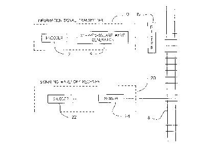
In Figure 1, information signal transmitter 10
generates a signaling waveform, which waveform can be
composed of a plurality of square wave signals onto which an
information signal is encoded. It is preferred that
information signal transmitter 10 be a switching-mode
transmitter. Transmitter 10 employs track rails 18 as the
signal transmission medium where signaling waveform receiver
20, preferably located in a cab of a railroad vehicle,
intercepts the signaling waveform and extracts an information
signal therefrom. In a present embodiment of the present
invention, it is preferred that transmitter 10 include a
stepped-square wave generator 14 which provides a signaling
waveform with information encoded thereupon, and which
transmits the signaling waveform through train rails 18. The
signaling waveform may be a multi-stepped carrier waveform
which, after being encoded, becomes a coded-carrier signal
for providing information to a railway vehicle.
It is also preferred to provide an encoder 12, for
generating the information signal. Stepped-square wave
generator 14 can include encoder 12 therewithin. Output
filter 16, preferably a tuned output filter, can be provided
for filtering harmonics from the stepped-square waveform and
2 1~ ~ 2 1 2
-
- 10 -
for isolating transmitter 10 from other signals which may be
present on track rails 18.
Signaling waveform receiver 20 can receive the
signaling waveform from track rails 18 using a sensor 24, for
example, a set of pick-up coils. Receiver 20 provides the
signaling waveform to information signal decoder 22, whereby
the railcar personnel can be apprised of the desired
information, and on-board control can utilize the vehicle
signal information.
Figure 2d illustrates a stepped-square wave 33 which
can be used to transmit information such as, for example,
railcar speed limit information. Wave 33 is a composite
waveform composed of the sum of the two waves 31 (Figure 2b)
and 32 (Figure 2c). Each of these two constituent square
waves 31, 32 have a specific amplitude, namely A1 and A2,
respectively, and duty cycle, namely P1 and P2, respectively.
A standard tool for analyzing periodic waves is the
Fourier Series, which allows any periodic wave to be
represented mathematically by the sum of its fundamental
frequency and all harmonics thereof, each of these frequency
components having a specific amplitude.
In Figure 2d, the Fourier Series of composite wave 33
can be represented in terms of the amplitudes and duty cycles
of its two constituent waves, 31 and 32:
21~8~
-
11
V(t)= ~ ~ 4 sin(m2~)¦Alsin(m ~2Pl ) +A2sin(m~2P2)]}sin(mZ~ ft)
where
A1, A2 are the amplitudes of the first and second
square waves 31 and 32, respectively;
P1 and P2 are the duty cycles of the first and second
square waves 31 and 32, respectively;
f is the fundamental frequency of wave 30 and 31;
m represents the harmonic order.
Likewise, for a standard "On-Off" square wave such as,
for example, wave 30 in Figure 2a:
V(t)= ~ ~m~} sin(m2~ ft)
where
A is the amplitude of wave 30,
f is the fundamental frequency of wave 30, and
m is the harmonic order.
The significance of these two expressions is that they
allow the harmonic content of wave 33 to be compared
mathematically with the harmonic content of a standard "On-
Off'~ square wave 30. For the invention herein, it is
preferred that duty cycle of first square wave, P1, generally
be between .60 and .90, particularly between 0.76 and 0.84,
with a preferred value of about 0.8, and that the duty cycle
of the second square wave, P2, generally be between .20 and
2l~21 2
- 12 -
.50, particularly between 0.38 and 0.42, with a preferred
value of about 0. 4. It is similarly preferred that the
amplitude of the first square wave Al generally be between
.80 and 1. 20, particularly between 0.95 and 1.05, with a
preferred value of about 1.00, and that the amplitude of the
second square wave A2 generally be between . 40 and .80,
particularly between 0. 594 and 0.656, with a preferred value
of about 0.625.
TABLE 1
"ON-OFF" SQUARE STEPPED-SQUARE
HARMONICWAVE AMPLITUDE WAVE AMPLITUDE
3 0-3333 0.0017
0.5000 0.0000
7 0.1429 0.0007
9 O.1111 0.1111
11 0.0909 ~~0909
13 0.0769 0.0004
0.0667 0.0000
17 0.0588 0.0003
In Table 1, the relative amplitude values of an
exemplary composite stepped-square wave are compared to the
relative amplitude values of a standard "On-Off" square wave,
at particular harmonic frequencies using Fourier analysis.
The values of the simulated stepped-square wave were produced
using the aforementioned preferred duty cycle and amplitude
2 1 ~ ~ 2 1 2
values. Table 1 indicates that this combination of duty
cycles and amplitudes essentially eliminates the energy
content normally associated with the third, fifth, and
seventh harmonics. While certain higher-order harmonics such
as the ninth and eleventh are substantially unattenuated
relative to a square wave, these frequencies generally have
lower energy content and can be far enough away from the
fundamental to be attenuated by a simple filter. By altering
the constituent wave amplitude and duty cycles, a different
mix of harmonics can be produced.
Figure 3a shows one present preferred embodiment of
signaling transmitter 50. Multi-tap transformer 62 employs a
plurality of drive switches 72, 74, 76, 78, to selectively
fashion an output voltage 63 of a preselected waveform on
output terminals 64. Drive switches 72, 74, 76, 78, which
are preferred to be semiconductor switches and more
preferably, field effect transistors, are operated by
synchronized timing signals which are selectively applied to
gate drive inputs 52, 54, 56, 58. DC input 60, which is
preferably a nominal 12 VDC battery, drives multi-tap
transformer 62 in a push-pull configuration.
Two taps can be placed on primary winding 66 to
produce an upper step in the voltage waveform. The amplitude
of the upper step can be a function of the turns ratio in the
primary windings. To substantially reduce the amplitude of
the specific harmonics, the ratios of the total number of
2 ~
- 14 -
primary turns with the number of turns at a particular tap
can be preselected. For example, to substantially reduce the
amplitude of the third, fifth and seventh harmonics, the
ratio of the total number of turns to the number of turns at
the first and second taps are preferred to be about 1.000 and
1.625, respectively. In addition, because the voltage
amplitudes of the step waveforms can be functions of the
turns ratios of the primary windings, the voltage amplitude
of a particular step may also be preselected. For example,
in the case where the first and second turns ratios are about
1.000 and 1.625, the amplitude ratios of the voltages at the
respective taps are about 1.00 and 1.62.
Figures 3b-f present exemplary gate timing diagrams
and a resultant waveform which can be created by signaling
transmitter 50 of Figure 3a, having four drive switches, 72,
74, 76, 78. In Figure 3b, drive signal 152 represents the
synchronized timing signal which can be applied by gate drive
input 52 to drive switch 72 in Figure 3a. Similarly, in
Figure 3c, drive signal 154 can be applied by gate drive
input 54 to drive switch 74. Drive signal 156 in Figure 3d
can be applied by gate drive input 56 to drive switch 76.
Also, drive signal 158 in Figure 3e can be applied by gate
drive input 58 to drive switch 78. The selective application
of such drive signals 152, 154, 156, 158 to drive switches
72, 74, 76, 78, respectively, produces resultant output
voltage 163, shown in Figure 3f across output terminals 64.
2 ~ ~
One preferred embodiment of a stepped-square wave
generator 100 is shown in Figure 4. Encoder 102 provides
encoded information signal 122 to synchronizer 106. Clock
104 generates clocking signal 124 at a predetermined
frequency, and also provides signal 124 to synchronizer 106.
Synchronizer 106 fashions from signals 122 and 124, input
drive signal 126 which can be used to operate switch driver
108. Alternatively, input drive signal 126 may be produced
by switching controller 101. In this case, switching
controller 101 can be responsive to encoded information
signal 122 from encoder 102. Switching controller 101 may
include clock 104 and synchronizer 106 therewithin. Switch
driver 108 selectively produces gate drive signal 128 to
signaling transmitter 110. Signaling transmitter 110
produces signaling waveform 130, which signaling waveform 130
has an information signal encoded thereupon. It may be
desirable to electrically isolate signaling transmitter 110
from other signals which may be present on track 116, in
which case tuned output filter 114 can be provided. Also,
current limiter 112 can be provided to prevent excessive
heating of the semiconductor switching circuits in signaling
transmitter 110 during high-current draw conditions such as,
for example, when a train is stopped on top of the track
connection. Information may be encoded by turning on and off
transmitter 100 at the preselected encoding rate of encoder
,.,, 2l~g2~
- 16 -
102. These encoding rates can be, for example, 75, 120 and
180 CPM.
Figure 5a illustrates encoder 302 and clock 304 which
are similar to respective encoder 102 and clock 104 shown in
Figure 4. Synchronizer 306 in Figure 5b is similar to
synchronizer 106 in Figure 4. Figure 5c illustrates switch
driver 308 which is similar to switch driver 108 in Figure 4.
Figure 5d illustrates signaling transmitter 310 which is
similar to signaling transmitter 110 in Figure 4. Signals
301, 303 and 305 in Figure 5a correspond to signals 301, 303
and 305 in Figure 5b. Signals 307, 309, 311, 313, 315 and
317 in Figure 5b correspond to signals 307, 309, 311, 313,
315 and 317 in Figure 5c. Signals 329, 331, 333, 335, 337,
339 and 341 in Figure 5c correspond to signals 329, 331, 333,
335, 337, 339 and 341 in Figure 5d. Signals 319, 321, 323,
325 and 327 in Figure 5b correspond to signals 319, 321, 323,
325 and 327 in Figure 5e. Signal 343 in Figure 5b
corresponds to signal 343 in Figures 5d and 5e.
In clock 304 of Figure 5a, oscillator 212 generates a
preselected frequency such as, for example, 1.8432 Mhz, which
is divided down by divide-by-N counter 214 to produce a
signal 305 at a desired frequency such as, for example, 600
Hz. Signal 305 is used to drive decade counter 216 in the
synchronizer in Figure 5b. Each of the 10 outputs 220-229
(Q0-Q9) of decade counter 216 provide clocking pulses at one
tenth of the frequency of signal 305, for example, 60 Hz.
2l ~&21,'?
- 17 -
Each of the outputs 220-229 (Q0-Q9) turns on at the same time
with respect to the other outputs 220-229 (Q0-Q9). For
example, at start-up, output 220 (Q0) will turn on first and,
when Q0 turns off, output 221 (Q1) will turn on. This
process continues through to output 229 (Q9), recommencing
the process by again turning on output 220 (Q0). Continuing
in Figure 5a, counter 214 in clock 304 may be programmed to
provide the desired carrier frequency. For example, where
the carrier frequency is desired to be 60 Hz, counter 214 can
be programmed to divide by 3072 to produce a 600 Hz output on
signal 305. Where a 100 Hz carrier frequency is desired,
counter 214 in clock 304 may be programmed to divide by 1843
thereby providing signal 305 with a frequency of 1000 Hz.
Code input 254 in encoder 302 allows the transmitter
to be turned on and off at preselected coding frequencies
such as, for example, 75, 120, and 180 CPM. The code signal
from input 254 passes through flip-flop 256 onto reset line
303 of decade counter 216, shown in Figure 5b. When the code
input 254 is high, only output 220 (Q0) of counter 216 is
high, all other outputs 221, 229 (Q1-Q9) are low, and the
transmitter is turned off. When code input 254 goes low,
counter 216 starts a pulse train on output 220 (Q0). It is
desirable that every time the transmitter is turned on, it
starts at the beginning of the cycle of counter 216. Flip-
flop 256 in Figure 5a controls the transmitter turn-off by
keeping reset line 303 low until output 220 (Q0) goes high.
21~21 ~
-
Because output 220 (Q0) is the end of the counter cycle, the
transmitter is turned off at the zero-crossing. This
produces an integer number of carrier cycles during the
carrier on-time. During the carrier off-time, primary
windings 274 in Figure 5d are shorted to ground by turning on
FETs 232, 246, 234, and 248. This is accomplished by counter
output 220 (Q0) which goes high when counter 216 is reset.
It is desirable to not permit primary windings 274 to be left
floating or unconnected.
The transistor gate drive signals may be derived from
the outputs 220-229 of counter 216 by selectively combining
outputs 220-229 using sequential logic devices including a
plurality of OR gates 217a-217p as illustrated in Figure 5b.
For example, to produce the drive signal for FET 231 in
Figure 5d, four outputs 221-224 (Q1-Q4) are OR-ed together,
as shown in Figure 5b. This generates a pulse or signal 307
that is on for 40~ of the cycle time. Switching drive
circuit 218a in switch driver 308 of Figure 5c drives FETs
231 and 233 by using FET driver 211a to invert signal 307.
Drive circuit 218a is provided power by battery 266 in Figure
5d to ensure full turn-off of the p-channel FETs 231 and 233
in Figure 5d. Similarly, switching drive circuit 218b drives
FETs 235 and 236 in Figure 5d.
Switching drive circuit 218c in Figure 5c can include
voltage comparator 219, along with a push-pull transistor
circuit 230, to drive FETs 232 and 246 in Figure 5d.
2158~
- 19 -
Similarly, switching drive circuit 218d in Figure 5c drives
FETs 234 and 248 in Figure 5d. The gate drive signals 280a
and 280b switch between +12 volts and -12 volts. The -12
volts is provided to overcome the negative voltage which may
be produced by transformer 272 in Figure 5d when FETs 232,
246, 234, and 248 are turned off.
Continuing in signaling transmitter 310 of Figure 5d,
two n-channel FETs 246, 248 are put in series with FETs 232
and 234, respectively, to block the flow of current in the
reverse direction through the internal diode when FETs 232
and 234 are turned off. The ground reference resistors 250,
252 are connected between the sources of FETs 232 and 234,
respectively, and ground thereby providing a ground reference
to keep the respective transistor sources from floating.
Transformer 272 is driven in a full-bridge
configuration from a nominal 12 volt battery 266. Two taps
268, 270 have been placed on primary windings 274 to produce
the upper step in the output waveform. The amplitude of the
upper step is a function of the turns ratio in primary
windings 274. The amplitude ratio of these two steps may be
manipulated to minimize particular frequencies. For example,
to substantially reduce the third, fifth, and seventh
harmonic frequencies, it is desired to provide an amplitude
ratio of the two steps to be approximately 1.00 and 1.62.
With relation to the number of turns in the primary, the
ratio may be determined such that the total number of primary
2~ ~82~ ?~
- 20 -
turns divided by the number of turns at the particular tap,
for example, tap 268 is approximately equal to the desired
amplitude ratio. For example, where the total number of
turns in primary 274 is about 104, and the number of turns at
tap 268 is 64 turns, the turns ratio will be about 1.625; the
associated amplitude ratio is about 1.62.
A current limiter circuit may be composed of a
voltage sensor, such as sense resistors 244a and 244b,
comparator 240 and flip-flop 242. When the voltage across
sense resistor 244a, 244b exceeds the trip point of
comparator 240, flip-flop 242 is triggered. The output of
flip-flop 242 in Figure 5e turns off FETs 231, 233, 235 and
236, and turns on FETs 232, 246, 234, and 248 in Figure 5d.
Flip-flop 242 is reset at the beginning of the next half-
cycle to return the circuit to normal operation. The current
limiting circuit 312 may be necessary to prevent excessive
heating of the switching FETs 231-236 when a train is stopped
on top of a track connection.
Figures 6a-g presents exemplary gate timing diagrams
and a resultant output stepped-square waveform which can be
created by the stepped-square wave generator illustrated in
Figures 5a-5d and current limiter 5e, and the description
relating thereto. Drive signals 401 (shown in Figure 6b),
404 (shown in Figure 6c), 406 (shown in Figure 6d), 403
(shown in Figure 6e), 402 (shown in Figure 6f), and 405
(shown in Figure 6g) are similar to drive signals 331, 337,
2~ 3 21~
341, 329, 333 and 339, respectively, in Figure 5d. In Figure
6b, FET drive signal 401 represents the synchronized timing
signal which can be applied to FET 231 in Figure 5d.
Similarly, FET drive signals 404, 406, 403, 402 and 405 in
Figures 6c-g represent the synchronized timing signal which
can be applied to FETs 234, 236, 233, 232 and 235,
respectively in Figure 5d. The selective application of FET
drive signals 401, 404, 406, 403, 402 and 405 produces
resultant output voltage 400, with the waveform having the
stepped-square wave morphology, characteristic of the
invention herein.
Also illustrated in Figure 6a is an exemplary
limiting of the waveform of output voltage 400 which may be
encountered during the operation of current limiter 312, in
Figure 5e, as previously described.
While certain present embodiments of the invention
have been illustrated, it is understood that the invention is
not limited thereto, and may be otherwise variously embodied
and practiced within the scope of the following claims.