Note: Descriptions are shown in the official language in which they were submitted.
~ 94~22142 2 f ~ ~ 4 ~ 7 PCT~S94/02885
P~Nn~M p~ M~M~py ~RAN) BASED CONFIG~Rr~ ARRAYS
BACKGROUND OF THE lN V~N'l'lON
This invention relates generally to field
S programmable gate arrays ("FPGAs"). Field programmable
gate or logic arrays usually store configuration data to
control the FPGA's configurable switches and
configurable logic blocks.
A problem with prior art FPGA chips is these chips'
high cost per logic gate. Another problem is the
lengthy period required for calculating the routing of
these configurable logic chips. One prior art FPGA chip
can take hours to route by computer. Yet another
problem with prior art FPGA chips is their poor gate
utilization. Because of the difficulties routing prior
art FPGA chips, generally only a small fraction of the
gates in a prior art FPGA chip are used for a given
circuit design. Another problem with prior art FPGA
chips is the poor visibility of the circuits placed in
these chips. It is difficult to observe the value of
certain nodes of the circuit placed on a prior art FPGA
chips. It is also difficult to externally set the
values of certain nodes of the circuit placed on the
prior art FPGA chips. This lack of ~isibility is
especially disadvantageous if the FPGA chips are used
for emulation. It is desired to have observability and
controllability of many locations in a circuit being
emulated and tested.
It is therefore an object of the present invention
to provide an FPGA chip which is cheaper in cost per
gate.
WO 94/22142 PCT/US94/02885 ~
21~8467
A further object of the present invention is to
provide an FPGA chip which requires less computer time
to route.
A still further object of the present invention is
to provide an FPGA chip with a high gate utilization.
It is desired that a larger percentage of the gates in
the FPGA chip be used for any given circuit design.
A yet another object of the present invention is to
provide an FPGA chip with better visibility and
controllability.
SUMMARY OF THE Ihvh~ ON
Some of the above objects of the present invention
can be achieved by an integrated circuit chip that uses
charge storage memory cells requiring a periodic
refr~chi~g of charge, such as dynamic random access
memory ("DRAM") based memory cells, associated with the
configurable switches and configuration bit buffers of
the logic blocks. DRAM is a very dense type of memory.
The small DRAM cells can be attached to the configurable
switches used to interconnPct con~lctors in the FPGAs
and to buffers used to configure the logic blocks.
DRAM based memory cells have in the past been
considered impractical for use in FPGA chips. DRAM
memory cells use capacitorc to store bits of data.
These capacitors must be refreshed periodically so that
the DRAN does not lose data. These DRAM cells are
refreshed by reading the value from the capacitor and
then rew,riting this value back into the capacitor. The
reading of the value of the capacitor in prior art DRAM
systems temporarily destroys the value in the capacitor.
For this reason, if the DRAM memory cell is attached to
a switch or buffer in an FPGA chip, the state of the
buffer or switch will likely change during the
refreshing of the memory cell. Others have suggested,
therefore, that it is necessary to include a separate
~ 94~22142 2 1 5 ~ ~ 6 7 PCT~S94102885
memory of the contents of each cell of an array of
charge storage cells in order ~o be able to periodically
refresh their states without disrupting the elements
that are set according to the memory cell states.
However, the present invention is able to use DRAM type
of cells in FPGAs in two possible manners without the
neC~city for such a duplicate memory.
According to one specific aspect of the present
invention, limitations are placed upon the type of
circuits that can be produced or emulated with the
FPGAs. If the type of circuits emulated or placed on
the FPGA only use flip-flops for storage elements,
rather than using the combination logic to
asynchronously store information, it is possible to use
a traditional DRAM memory cell directly connected to
switches and/or buffers in the FPGA. Even when
limitations are placed on the emulated circuit, the FPGA
must make sure that the system clock of the circuit
emulated in the FPGA is not set within the period of
time of the longest propagation delay of a signal going
from one flip-flop storage element to another flip-flop
storage element after the DRAM based memory cells are
refreshed.
According to another and preferred specific aspect
of the present invention, the traditional DRAM hA~e~
memory cell portion of the switching cell is modified in
one of several particular ways and directly coupled with
a switching transistor or input of a buffer or inverter.
This results in the switching cell maint~in; ng, during
its periodic refreshing, the state of the switches and
configuration data buffers that are set according to
that state.
One way to accomplish this result is to use a
larger capacitor than normally used in a DRAM memory
cell. By using this larger capacitor, the voltage at
the switch or buffer can be maint~inp~ during refresh,
W094/~142 PCT~S94/02885 ~
21~8~7
, .
above or below the switching point of the driven switch
or buffer In addition, the writing time period of the
refresh cycle of the DRAM based memory cell can be
~YrA~ed to accommodate slower write ~ack into the
larger capacitor.
Alternatively, a resistive element can be added to
the DRAM based memory cell having the same size
capacitor as normally used. This resistive element can
510w the discharge of the capacitor in the memory cell
so that DRAM circuit can write back the value to the
capacitor before the value in the capacitor reaches a
switching point of the transistor. The resistor can
also be combined with the use of a larger capacitor than
normal.
Another embodiment of the present invention is to
use two capacitors in the DRAM cell. These two
capacitors are separated by a resistive element. The
first capacitor which is closer to the access transistor
of the memory cell can be read in a manner similar to a
manner that a capacitor is read in the normal DRAM
memory cell. The second capacitor, separated by the
resistive element, is not read as quickly so that the
switch or buffer connected to this second capacitor does
not switch its state. The write time of the refresh
cycle is increased so that both of these capacitors are
charged up to the correct value in the write-back.
Furthermore, if the process is asymmetric, that is,
if the writing of a logical "zero" or a logical "one" to
the second capacitor takes more time. A leaky diode can
be used to speed up either the writing of the logical
"zero" or logical "one" into the second capacitor.
Additionally, multiple diodes can be used between
two capacitors, one set of the diodes biased in one
direction and the other set of diodes biased in the
other direction. The use of these diodes can be used to
~ 94/~2142 2 PCT~594/U2885
prevent the pre-charging of the column from affecting
the value at the second capacitor.
Of course, other changes can be made to the DRAM
cell consistent with the present invention in order to
maintain its state during a read and refresh operation.
The benefits of using a DRAM based memory cell
include a lower cost per gate. DRAM chips are very
cheap to produce so the benefit of using a modification
of the DRAM cell is that it is likely that a DRAM based
memory cell used in an FPGA chip will cause the FPGA
chip of the present invention to be cheaper per gate
than other prior art FPGA chips. Additionally, DRAM
based memory is very dense. In present process
t~chni~ues~ the density of DRAM memory cells are limited
by the metallization widths. The above discussed
additional elements should not require a larger memory
cell area. The access lines to the DRAM based memory
cell units can be interspaced with interconnection lines
also made of the metallization layers. Due to the
increased density of the switches, a greater number of
switches can be used in the FPGA chip of the present
invention. This means that architectures that are
derivative of full cross-point architectures can be
used. These type of architectures use more switches for
interconnection but are logically easier to
interconnect. This means that the gate utilization of
the FPGA will be increased and the computer time used to
route the FPGA can be reduced. The reduction of the
routing time is especially beneficial for emulation
applications of the FPGA chips.
According to yet another aspect of the present
invention, the random-access-memory ("RAM") is provided
with the capability of accessing nodes of a configured
switching network or logic circuit through the memory
array for the purpose of monitoring signals at some
nodes (visibility) and forcing signals at others
WO94/22142 ~ 6~ PCT~S94/02885 ~
(controllability). This benefit does not require the
use of the dynamic type of RAM -ells but a DRAM array is
usually preferred because of its high density, low cost
per bit, and other advantages discussed above. An
example of nodes with which the observability feature
can be used, for example, are inputs and outputs of
selected logic blocks. An example of the use of the
~u.lLrollability feature is to set and reset flip-flops
of a configured circuit. Use of the controllsbility and
observability features allow for a high level of
visibility and control that is particularly desirable
when emulating an actual logic circuit or testing a
particular circuit design that is configured on the
chip. Because a circuit being emulated or tested is
easily and rapidly reconfigurable, in total or in part,
by randomly accessing and programming controlling memory
locations (as opposed to existing systems requiring the
lo~ of an entire serial bit stream in order to alter
the configured circuit), the connections and logic
functions of the configured circuit can easily and
~uickly be edited.
An additional benefit of the present invention
concerns the use of the row and column decoder to set
values in the emulation. The memory cells can be
located right at the switch and buffer locations and the
row and column lines of the ~co~r can be interleaved
with the interconnection lines used for the switching
between the logic gates.
BRIEF DESCRIPTION OF THE DRAWINGS
The above and other features and aspects of the
present invention will become more apparent upon reading
the following detailed description in conjunction with
the accompanying drawings, in which:
~ 94/22142 PCT~S94/02885
~1S;B46~7
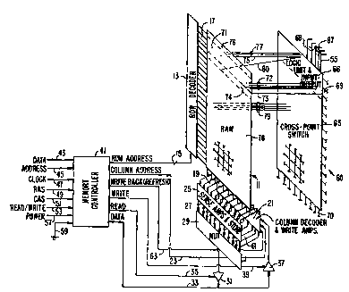
Fig. 1 shows the functional elements of a complete
integrated circuit system that embodies various aspects
of the present invention;
Figs. 2A and 2B show two integrated circuit chip
layouts of example switching cells included within the
integrated circuit of Fig. l;
Fig. 3A shows an integrated circuit chip layout of
an example logic unit included within the integrated
circuit of Fig. l;
Fig. 3B is a diagram of the circuit implemented by
the layout of Fig. 3A;
Fig. 4 shows an integrated circuit chip layout of
another example logic unit included within the
integrated circuit of Fig. l;
Fig. 5 shows an integrated circuit chip layout of an
input/o~L~uL unit included within the integrated circuit
of Fig. 1;
Fig. 6 is a schematic view of the prior art DRAM
cell;
Fig. 7 is a graph of the voltage at the capacitor of
the memory cell of Fig. 6 for a logical "one" and
logical "zero" during the leakage, the read and the
write period of the memory cell;
Fig. 8 is a schematic view of one embodiment of the
present invention showing memory cell consisting of an
access transistor and a capacitive element connected to
a switch interconnecting two lines;
Fig. 9 is a block diagram showing a section of an
emulated circuit on the FPGA plus the interlock
circuitry required for the use of the memory cell type
shown in Fig. 8;
Fig. lO is a timing diagram used to explain
limitations on the use of the memory cell shown in Fig.
8;
W094/22142 PCT~S94/02885 ~
2l~8~
Fig. llA is a schematic view of an embo~;m~nt of the
present invention using a memory cell with a large
capacitive element;
Fig. llB is a schematic view showing some pre-charge
circuitry including an inherent capacitance C~ which is
connected to the memory cell including the capacitive
element C,;
Fig. 12 is a graph of the voltage at the capacitor
of Fig. llA showing the voltage at this capacitor for a
logical "one" and logical "zero" during the leakage,
read, and write periods;
Fig. 13A is a schematic diagram of an embo~;~?nt of
the present invention showing a memory cell with a
resistive element located between the capacitor and the
access transistor;
Fig. 13B is a schematic view of an embodiment of the
present invention showing a resistive element placed
between the column and the access transistor;
Fig. 14 is a graph of the voltages at the capacitor
in Fig. 13A and 13B for a logical "one" or a logical
"zero" during the leakage, read, and write periods;
Fig. 15 is a schematic view of still another
embodiment of the present invention showing two
capacitors in the memory cell separated by a resistive
element;
Fig. 16 is a graph of the voltage at capacitor A for
a memory cell of Fig. 15 for a logical "one" or logical
"zero" during the leakage read and write periods;
Fig. 17 is a graph of the voltage at capacitor B of
the memory cell of Fig. 15 for a logical "one" or
logical "zero" during the leakage, read, and write
periods;
Fig. 18 a schematic view of yet another embodiment
of the present invention showing a capacitor A and B
separated by a leaky diode;
94/22142 ~ S ~ PCT~S94102885
Fig. 19 is a graph of the voltage at capacitor A in
the memory cell of Fig. 1~ for a logical "one" or
logical "zero" during the leakage, read, or write
period;
Fig. 20 is a graph showing the voltage at capacitor
B of the memory cell of Fig. 18 for a logical "one" or
logical "zero" during the leakage, read, and write
period;
Fig. 21 is still yet another embodiment of the
present invention showing a memory cell with a capacitor
A separated from capacitor B by two sets of diodes
biased in opposite directions;
Fig. 22 is a graph of the voltage at capacitor A of
the memory cell of Fig. 21 for a logical "one" or
logical "zero" during the leakage, read, or write
period;
Fig. 23 is a graph of the voltage at capacitor B for
memory cell of Fig. 21 for a logical "one" or logical
"zero" during the leakage, read, or write period;
Fig. 24 is a schematic view of an embodiment of the
present invention showing a memory cell having two
capacitors and two transistors;
Fig. 25 is a schematic view showing the
metallization layers used for the memory cell of Fig.
2s 24;
Fig. 26 is a schematic view showing a memory cell of
the present invention connected to a buffer;
Fig. 27 is a schematic view of one bit of an
observability line;
Fig. 28 is a schematic view of one bit of the
controllability line; and
Fig. 29 is a schematic diagram of a logic unit that
includes a flip-flop as well as observability and
controllability features.
WO94/22142 PCT~S94/02885 ~
-^ ~iS~ 4~rt
~ESCRIPTION OF THE PREFERRED EMBODIMENTS
Although a system embodying the various aspects of
the present invention can be implemented with two or
more integrated circuit chips, either in separate
packages or a single package, it is certainly preferable
from a cost and utilization standpoint to do so on a
single chip in its own package. The primary functional
components of such a system implemented on a single chip
are illustrated in Figure 1. A RAM ll follows a usual
design of providing a two dimensional array of memory
cells, one at each intersection of row and column
conductors.
A row decoder 13, in response to a row address in a
bus 15, selects a designated one of a plurality of row
conductors 17 (word lines) to enable the r~A~;n~ from or
writing to one or more of the memory cells connected to
that row line. R~A~; ng from or writing to one or more
of these memory cells at a time is accomplished by
applying a proper voltage to those of a plurality of
column lines 19 to which the desired cell(s) are also
connected. For writing, a desired column or columns, to
which the desired cell or cells are connected, are
selected by a decoder 21 in response to an address on a
column address bus 23. The column ~Pco~Pr block 21 also
includes one or more write amplifiers for driving the
selected addressed column line or lines. Similarly,
sense amplifiers 25 are also connected to the column
lines 19, usually a separate sense amplifier for each
column line, the G~L~u~s of which are applied by lines
27 to a multiplexer 29 that selects one or more of the
sense amplifier outputs in response to an address on the
column address bus 23. The sense amplifiers 25 and
multiplexer 29 allow reading any of the memory cells in
a row whose row line 17 is properly energized and which
are addressed by the multiplexer 29. An output of the
multiplexer 29 is received ~y a gated amplifier 31 that
~ 94/22142 ~ PCT~S94/02885
- ~S8~67
provides an output in a data line 33 in response to a
read control signal in a line 35. The individual sense
amplifiers 25 are also designed to store, at least
temporarily, the voltage level of their respective
column lines. Another gated amplifier 37 receives a
signal from the data line 33 and applies it to the
column decoder and write amplifier block 21 in response
to activation of a write signal in a line 39.
A memory controller 41 of a typical design is also
included on the chip. The controller 41 connects the
chip of Figure 1 to other components in a larger system
through package pins that include the following: a data
bus 43, an address bus 45, a clock signal 47, a row
address strobe ("RAS") signal 49, a column address
strobe ("CAS") signal 51, a read/write control signal
53, and power pins 57 and 59.
A preferred form of the RAM 11 is the previously
~i~rl.Cc~ DRAM because of the very high packing
densities that are currently state of the art and its
relatively low cost. Further, DRAM integrates nicely
with an array 60 of conductors and configurable logic
units which are selectively interconnected by field
effect transistor ("FET") switches and configured,
respectively, under ~ollLlol of the contents of memory
cells within the memory array 11. Many aspects of the
present invention can be implemented, however, with
other forms of RAM, such as static RAM ("SRAM"),
electrically erasable and programmable read only memory
("EEPROM"), or some other form of non-volatile memory.
However, with the preferred choice of DRAM, the memory
system must include the usual ability to periodically
refresh the state of the memory cells. That is, since
DRAM cells store either a 0 or 1 corresponding to a
charge level stored on a capacitor within each cell,
that charge leaks off over time. In the system of
Figure 1, conductors 61 apply the individual outputs of
W094/22142 PCT~S9~/02885 ~
?~ ~5
the read amplifiers 25, by connection to the individual
lines 27, to inputs of the writing amplifiers within the
block 21. In response to a refresh control signal in a
line 63, the outputs of the read sense amplifiers, as
temporarily stored therein, are applied back to the same
column lines of the array 11 from which they were just
read, through the writing amplifiers 21. Thus, an
entire row of cells within the array 11 is refreshed at
a single time. The refresh proces~, as is well known,
first reads the states of cells within a designated row
addressed through the row decoder 13, causing the charge
in the cell's capacitors to be further discharged, and
then immediately recharges the capacitor to its full
state by the refresh process. Further details of the
refreshing process and individual cell construction is
explained below with respect to Figures 6 and 7. The
known t~h~; ques of refreshing DRAMs are numerous.
There are also many known DRAM system architectures.
The array 60, in the example of Figure 1, is shown
to be arranged in two functionally different sections or
portions 65 and 66. The portion 65 includes rows and
columns of conductors, either continuous or broken into
segments, with switching transistors co~ne~ted to
selectively interconnect columns and rows of conductors,
and/or connect segments of such rows and columns
together in various configuration segments.
The second portion 66 of the array 60 includes
configurable logic units and configurable input-output
circuits that are conna~ted to receive and send signals
on column conductors ext~e~ from the portion 65 of the
array 60. Thus, the interconnecting FET switches within
the array portion 65 interco~ects signals between the
various logic units and input-output circuits within the
array portion 66. Of course, logic units can
alternatively, or additionally, be co~n~cted to row
conductors within the array portion 65. A rather simple
~ 94/22142 PCT~S94/02885
~ S
~6
13
system architecture has been chosen for illustration as
a basic for explaining the principles of the various
aspects of the present invention and their preferred
implementation.
Conductors 67 illustrate signal outputs of circuits
in the array portion 66, and are connected to external
pins on the package. Similarly, some external package
pins are connected to input lines 68 to the circuits.
Alternatively, external connections, such as line 55,
can be bi-directional with their function set upon
configuration of their respective input-output circuits.
Conductors 69 and 70 are extensions of the row and
column conductors, respectively, of the array 60. These
optional extensions allow connection with similar
conductors of other arrays in order to ~Yr~n~ the system
further, either on a single chip, or on multiple chips,
either within a single package or in separate packages.
The types of logic units that may be included in the
region 66 are many. In the specific simplified example
being described herein, two types of logic units are
used, both of which are configurable. A first is a
logic gate having a look up function with two inputs and
one G~L~L, the function of the gate being configurable
as st~n~Ard gate types such as OR, AND, NOR, exclusive
OR, and so forth. More complex gate stru~LuLe , such as
those with more inputs and/or ouL~uLs can also be
included. Any logic function can be implemented,
including, in addition to the functions listed above, a
multiplexer, a transistor, a tri-state buffer, and
others. The second type of logic unit illustrated in
this example is a D-type flip-flop. A preferred logic
unit includes a four input, one output look-up logic
function, one flip-flop and a tri-state driver, as
described below with respect to Fig. 29. Input-output
circuits within the portion 66 of the array 60 include
proper buffering and control portions to interface
WO94/22142 PCT~S94/02885 ~
84~
14
between column lines of the array 60 and outside
signals.
The logic units are configurable by loading the
proper states into associated memory cells of the array
11. A portion 71 of the memory array 11 contain cells
whose outputs are connected, such as by four line 72
from four memory cells, to one of the configurable gate
logic units contained within the region 66 of the array
60. An example of such a logic unit is described below
with respect to Figure 4. In addition to the four
configuration signal lines 72, another line 73 connects
the output of a memory cell within another region 74 of
the memory array 11 that allows signal nodes within the
configured logic units to be accessed through the RAM
array 11.
A flip-flop logic unit within the array portion 66
is also configured by the state of a memory cell within
the portion 71 of the RAM array 11, that state being
communicated over a line 75. Another portion 76 of the
RAM array 11 contains memory cells which may be written
to for the ~uL~ose of forcing the state of the flip-flop
logic units, signals to do that being communicated from
the memory cells to the flip-flop logic unit over lines
77. The memory ~ells in the portion 76 provide a
cullLlol of the operation of the logic units within the
array portion 66, as opposed to configuring their
connection or function.
Similarly, the individual switching transistors
within the portion 65 of the array 60 is controlled to
be in an on or off state by the state of one of the
associated memory cells within a region 78 of the RAM
array 11. Lines 79 are shown in Figure 1 to communicate
the states of four of these memory cells with four
respective switching transistors in the portion 65 of
the array 60.
~ 94/22142 ~ PCT~S94/02885
~.~
The two arrays 11 and 60 of separate rows and
columns of electrical conductors ar~ shown in Figure 1
to be separate in order to illustrate their separate
functions. The array 60 includes a large number of
Swit~h; ~g transistors whose states are controlled by
contents of individual memory cells within the array 11.
However, these two arrays are, according to the present
invention, superimposed on each other across a common
area of the semi-conductor substrate. The layout of
different portions of this combination are conceptually
illustrated in Figures 2A-5.
Switchinq Cell and Confiqurable Loqic Cell ArraY
Figure 2A illustrates, in a plan view across an
integrated circuit surface, four adjacent cells of the
cross-point switches within the region 65 (Figure 1) and
their associated controlling memory cells 81-84 (Figure
2A) which reside in the portion 78 of the array 11. The
state of each of these memory cells 81-84 controls
whether each of the respective switching transistors 85-
88 is conductive or not. Each of the memory elements isprogrammable through its array of conductors, shown in
Figure 2A to include column conductors M1 and M2, plus
row con~llstors M3 and M4. Each of the memory elements
81-84, as is clear from Figure 2, is connected to one of
these column conductors and one of these row conductors
in order that they can be individual addressed for
reading, writing and refreshing.
The switc~;ng network of Figure 2A is formed by
column conductors S1 and S2, and row conductors S3 and
S4. It may be noted from Figure 2A that each of the
switching transistors 85-88 is connected to one of these
column conductors and one of these row conductors. A
connection between crossing row and column conductors is
made by energizing the gate of the switching transistor
connected to these conductors.
W094122142 2 ~ S ~ ~ ~ PCT~S94/02885
In the example of Figure 2A, the rows of conductors
from both of the arrays, namely conductors S3, M3, S4
and M4 are formed in a single metal layer within the
integrated circuit structure. Similarly, the column
conductors Ml, Sl, M2 and S2 are formed on a second
metal layer insulated from the first. Thus, the
conductors of each of the arrays ll and 60 (Figure l)
are combined on each of the two metal layers in the
integrated circuit structure. Each of the four cross-
point switching cells illustrated in Figure 2A thus hastwo column lines and two row lines passing through it.
Because of the simplicity and compactness of existing
DRAM technology, each of the memory cells 81-84 is very
small, which results in each of the four combined cells
of Figure 2A being very small. Tn~e~, the limit of how
small each of these cells can be made is that of the
pitch of the metal conductors. Thus, it may be
desirable to form a third, and even a fourth metal layer
in order to further vertically stack the conductors of
Figure 2A in order to reduce the amount of area taken by
each of the switching cells.
The type of switching array illustrated in Figure
2A, if ext~A~ throughout the portion 65 of the array
60, provides a full cross-point (cross-bar) switch.
That is, any column conductor can be connected to any
row ron~-~ctor. Thus, logic units within the region 66
of the array 60, which are connected to the column
conductors ext~n~;ng from the switching portion 65 to
carry signals between configured logic units, can be
connected to any other column conductor through the
large number of row conductors. ~his is desired in
order to provide maximum flexibility in implementing a
planned interconnection of logic units, and thus reduces
the complexity of determining the values to be loaded
into the individual memory cells in order to make such
connections.
~'094/22142 PCT~S94/02885
~sd~
17
However, a full cross-point switching network does
reguire a large area on the integrated circuit, an area
which can be re~t~c~A in appropriate circumstances by
reducing the number of row conductors within the portion
65 to less than the number of column conductors, or some
other appropriate arrangement. Such a reduction then
generally means that the job of designing a routing path
between logic units to form a specific circuit becomes
more difficult and time consumingO
It may be desirable in certain applications of the
full cross-point switching array discussed above to be
able to break some or all of the column and row
oon~llctors into isolated segments. This is especially
desirable, however, when a full cross-point switching
network is not provided since a single conductor can
then be used to carry more than one signal in its
separate segments. A layout of such a circuit is
illustrated in Figure 2B, which is shown as a
modification of the layout of Figure 2, all elements
identified by the same reference number having a prime
(') added. Instead of the transistors 85-88 (Figure 2A)
selectively interconnecting row and column conductors
together, transistors 85'-88' are connected in the path
of the various row and column conductors. Each such
con~ctor is then maintA; n~ as one, or separated into
two segments, dep~nA; ng upon the value stored in its
transistor switch controlling memory cell.
The present invention may also be used to implement
various other conductor connection arrangements that are
utilized in commercially available FPGAs where full
cross-point connectivity is not provided. An example is
a switching network including a number of individual
switching transistors that can be ~L~y dmmed in a manner
to form any combination of connections between three or
more pairs of conductors. In such an application, each
switching transistor of such a network has a state
WO94/22142 21~ ~ ~ 6 ~ PCT~S94/02885 ~
18
controlled by the contents of an associated storage cell
of the DRAM array.
Referring to Figure 3A, an example of a logic unit
cont~;~e~ within the portion 66 of the array 60 (Figure
l) is illustrated. For simplicity, a configurable logic
gate having two inputs IN0 and INl, carried on two
column conductors, and a single output signal OUT
carried by another column conductor. The signal
conductors extend into the cross-point switch portion 65
of the array 60 and are there connected to other logic
units within the region 66 through the switching
network. Column conductors M5, M6 and M7 are part of
the memory array ll, as are row conductors M8 and M9.
Another row conductor Ol is within the observability
array portion 74 of the memory array ll.
The function of the simple logic circuit illustrated
in Figure 3A is configured by the contents of four
memory cells 89-92 of the RAM array ll (Figure l). That
function is illustrated in a block circuit diagram of
Figure 3B, which uses the same reference numbers.
Effectively, the four possible combinations of digital
input signals in column conductors IN0 and INl operate
a multiplexer circuit 56 shown to select the contents of
one of the memory cells 89-92 for presentation at the
OUT conductor. Whether the circuit functions as an OR,
AND, or some other logical function, ~on~c upon the
contents of these four memory cells. Logic units form
to accommodate a larger number of inputs than the two
inputs illustrated use more memory cells to configure
their function. For example, as can be seen by
reference to Figure 3B, the preferred four input (the
inputs IN0 and INl shown, and additional inputs IN2 and
IN3 not shown) logic unit utilizes an increased capacity
multiplexer 56 in order to be able to switch between a
total of up to sixteen memory cells. Alternative to the
te~n;~ue used to implement a logic unit in the example
94/22142 PCT~S94/02885
19
of Figure 3B, a technique of storing a logic look up
table in a two dimensional array of memory cells may
also be utilized but is not preferred.
It will be noted that each of the memory cells 89-92
of Figure 3B drives one of the buffers 93-96. Rather
than connecting the memory cell directly to the
switçh; ng transistors, as is done in the switch;ng
network examples of Figures 2A and 2B, it is necessary
to provide a source of current along with each of the
memory cells when they are of the DRAM type. As
illustrated and discussed below, drawing current out of
such a memory cell rapidly depletes the charge stored in
the cell and can quickly change its state. Thus, the
charge stored in each DRAM cell, where an output current
is required, is connected to a buffer in order to
control the buffer~s output current between two levels
dep~n~ing upon the level of charge stored in the memory
cell.
The observability feature of the present invention
is also illustrated in Figure 3A, implemented with a
switch; ng transistor 97 connected between the output
column conductor OUT and one of the memory array column
conductors M7. The transistor 97 is rendered conductive
or not ~r~ ing upon the voltage on the RAM array row
line Ol. Thus, when the row line Ol is addressed
through the row ~co~ 13 (Figure 1), the output of the
circuit of Figure 3A is connected to the column line M7.
This then allows a selective observing or monitoring of
this output through the RAM array ll. Because of the
easy random accessibility of such an array, signals on
internal nodes of the configured circuit may be easily
aCc~cs~ and observed.
Figure 4 shows another type of logic unit which may
be utilized within the portion 66 of the array 60
(Figure 1), namely a D-type flip-flop. A flip-flop
circuit 98 has its Q output connected to an OUT column
WO94/22142 ~ ~ PCT~S94/02885 ~
~15~4~
conductor and its D input connected to a D column
conductor. A clock input to the flip-flop 98 comes from
another column conductor identified by CLK. A signal to
either preset or clear the flip-flop 98 is applied from
another column conductor indicated by PRE/CLR through
the logic elements shown. Whether an active signal on
the PRE/CLR column conductor causes flip-flop 98 to
preset or clear itself is determined by the state of the
memory cell 1 which conditions the clear and preset
signals through an inverter 4 and various logic elements
shown.
Two additional memory cells 2 and 3, driving
respective buffers 5 and 6, allow the flip-flop 98 to be
forced into either a cleared or a preset state without
affecting the configuration set by the contents of the
memory cell 1. The memory cells 2 and 3 are both
connected to a row cQn~llctor C1 of the controllability
portion 76 of the RAN array 11. These memory cells 2
and 3 can be randomly accessed and their contents
changed when it is desired to control the operation of
the flip-flop 98. As an alternative to the
controllability memory cells being connected to a common
row (word) conductor, as shown in the drawings, they can
be dispersed among the configuration logic memory cells.
2S There is a distinction between the configuration and
controllability functions performed by the example
circuits of Figures 2A-4. Bits stored in configuration
memory cells either establish connections that form a
circuit over which signals travel or conditions how the
circuit will respond to a given signal. The state of
the memory cells in the circuit of Figures 2A and 2B
directly establish circuit connections. The state of
the memory cells in the circuit of Figure 3A sets up the
logic transfer -function between its inputs and its
ouL~uL. The state of the memory cell 1 of Figure 4
conditions the circuit to respond in a particular way to
~0 94/22142 2 1 5 ~ 6 ~ PCT/US94,02885
an active signal in the PRE/SET line. Bits stored in
controllability memory cells, on the other hand, set
values of signals within the established circuit. Bits
written into the cells 2 and 3 o~ Figure 4, for example,
will force the flip-flop 98 into a predetermined state,
thus controlling the state of its output signal on the
conductor OUT.
The circuit of Figure 4 also includes an
observability function. A FET switch 99 interconnects
the output of the flip-flop 98 to a memory array column
line M13. The gate of the FET 99 is connected through
line 80 to a memory row conductor 02. Thus, when the
state of the signal on the row 02 becomes active, the
output of the flip-flop 98 may be read through the
memory array. This is a significant advantage when
testing or emulating a circuit that is configured on the
chip. It is important to be able to determine the
states of flip-flops internal of the operating circuit.
Although the example circuit layouts conceptually
illustrated in Figures 3A and 4 cause their respective
observability transistors 97 and 99 to be conductive by
signals on separate memory row lines 01 and 02, they can
be combined to respond to a single row line. Indeed,
many such observability FET switches can be controlled
by the signal on one row line. The result is the
simultaneous access through a number of column lines of
signals at a number of internal circuit nodes.
It will also be noticed that the example circuits of
Figures 3A and 4 alternate memory and logic circuit
column conductors across their layouts. This is usually
the most convenient arrangement, even though not all the
memory column conductors are used (such as M12 in Figure
4), since those unconnected to one logic unit will be
connected to another.
Figure 5 conceptually shows a layout for an
input/o~L~u~ circuit of a type that can be repeated in
WO94/22142 ; ~ ~6~ PCT~S94/02885
the region 66 of the array 60 (Figure 1). The conductor
55 connects with a circuit chip pad 7, which can serve
as either an input or an output to the circuit being
configured on the chip, in response to the value of a
control bit on a CONT. IN column line from outside of
the circuit of Figure 5. If operating as an output
circuit, a signal on the DATA OUT column conductor from
some other configured logic unit is transferred onto the
column conductor that is connected to the pad 7. If
operating as an input circuit, the signal on the pad 7
is transferred to a DATA IN column conductor for use by
some other configured logic circuit on the chip.
Memory cells 8 and 9 provide the primary
configuration information for the circuit of Figure 5
when being used to provide an output. The content of
the memory cell 8 configures the circuit to accept a
particular polarity of signal on the DATA OUT column
conductor, by providing one input to an exclusive OR-
gate 10 whose other input is the DATA OUT signal. The
gate 10 collL~ols, through a multiplexer 12, the gates of
output transistors 14 and 16. Transistors 14 and 16 are
connected in a series circuit, with additional
transistors 18 and 20, across the power supply voltage.
The value of the signal on the DATA OUT conductor thus
drives, through the gate 10 and multiplexer 12, an
ouL~L of this series transistor circuit in a line 22
co~n~cted to the column conductor to which the pad 7 is
connected.
This ou~uL function will operate only, however,
when the control bit on the CONT. IN column line
designates the output function. It does this by a
conn~ction, through a multiplexer 24, to the gates of
the transistors 18 and 20. When these transistors are
turned off, no output is provided on the line 22, but
when turned on, allows the circuit to provide an output
to the pad 7. The signal to the transistor 20 is
~ 094/~142 ~I ~ 8~6 7 PCT~S94/02885
selectively interrupted by a gated buffer 26, depending
upon the content of the memory cell 9. This then allows
the output 22 to be configured as an open collector
output when the bit in the memory cell 9 causes the
transistor 20 to be turned off while the signal on the
CONT. IN column conductor causes the transistor 18 to be
turned on.
Memory cells 28 and 30 provide an output circuit
controllability function. The multiplexer 12, in
response to a configuration bit in a memory cell 32, can
select the content of the memory cell 28 as the signal
to be provided as an output, in place of the actual
signal in the DATA OUT column conductor. Similarly, the
multiplexer 24, in response to a configuration bit in a
memory cell 34, can substitute the content of the memory
cell 30 as a control signal in place of an actual
control signal on the CONT. ~N column conductor.
When it is desired to operate the circuit of Figure
5 as an input circuit, the control signal on the CONT.
IN conductor i5 set to that which maintains the
transistors 18 and 20 in their off (non-conductive)
states, or the multiplexer 24 selects the content of the
memory 30 to turn off the transistors 18 and 20. Any
signal on the pad 7 then passes through an exclusive OR-
gate 36 and a multiplexer 38 to the DATA IN columnconductor for use as an input signal to some other
configured logic unit. A configuration bit in a memory
cell 40 adapts the circuit for the polarity of the input
signal. A c~rlLLollability bit in a memory cell 42 may
be substituted for such an actual input signal, in
response to the content of a configuration memory cell
44.
Observability of signals on certain conductors
within the circuit of Figure 5 is provided by
transistors 46, 48, 50 and 52. Each of these
transistors is rendered conductive or non-conductive by
WO94/22142 - PCT~S94/02885 ~
21~4~
24
the signal on a memory row conductor M22. When these
transistors are conductive, the signal on the DATA OUT
conductor is connected to a memory column conductor M15,
the control signal on the CONT. IN conductor to the
memory array conductor M16, the signal on the pad 7 to
the memory conductor M17, and the input signal on the
DATA IN conductor to the memory conductor M18. With
this arrangement, the memory column conductors M15, M16
and M17 are used at different times to both access the
memory cells connected to them and allow signals on
conductors of the circuit to be observed over them from
outside of the integrated circuit chip.
MemorY Cell Desiqn
A variety of different types of DRAM based memory
cells can be used in the structures of Figs. 1-5. A
discussion of prior art DRAM memory cells is relevant
here.
Fig. 6 is a schematic view of the prior art DRAM
memory cell 101. Memory cell 101 comprises an access
transistor 103 that has its gate connected to a row line
105 and its source connected to column line 107. The
drain of access transistor 103 is connected to a
capacitive element 109. This capacitive element is
typically formed out of a trench capacitor.
The row line 105 and column line 107 are usually
metal lines formed in metallization steps~ In DRAM
memory systems, the capacitive element 109 loses charge
due to a leakage to the substrate. For this reason, the
value in the capacitor 109 needs to be refreshed
periodically. In a refresh operation, the column line
107 is precharged to a voltage value between the voltage
corresponding to logical "one" and the voltage
corresponding to logical "zero". Typically, five volts
corresponds to logical "one", zero volts corresponds to
logical "zero", and the precharge voltage is 2.5 volts.
~ 094122142 2f S8~67 PCT~S94/02885
As described below, it is understood that the FPGA chips
of the present invention may use a lesser voltage for
the logical "one" case. It typically takes about 50ns
to precharge column line 107. After column line 107 is
precharged, the voltage at the row line 105 is set high
turning on the access transistor 103.
The activity of the DRAM cell 101 during the read
and write-back periods is best described with respect to
Fig. 7. Fig. 7 is a graph of a voltage at the capacitor
of the memory cell of Fig. 6 for logical "one" and a
logical "zero" during the leakage, the read and the
write period of the memory cell 101. The time scale of
this graph and the graphs of Figs. 12, 14, 16, 17, 19,
20, 22, and 23 is distorted. The leakage period is much
greater than the read or the write periods. The leakage
period or the longest period of time in between
refreshes of the capacitor 109 is illustratively around
4 milliseconds. The voltage at the capacitor 109 of the
memory cell 101 of Fig. 6 is shown in Fig. 7 as being a
continuous line for the logical "one" case and is shown
as a dotted line for the logical "zero" case. As shown
in Fig. 7, the voltage at the capacitor 109 during the
leakage period slowly lowers in the logical "one" case
and raises for the logical "zero" case. ThiS voltage
change is due to the leakage of charge on the capacitor
through the substrate. The precharging of the line 107
of the DRAM memory cell 101 is not shown in the graph of
Fig. 7. The precharge period occurs right before the
read period.
When the read period begins, access transistor 103
is turned on. In the logical "one" case, charge from
the capacitor 109 goes to the column line 107 and in the
logical "zero" case charge from the column line 107 goes
to the capacitor 109. A slight change of the voltage on
the column line 107 is se~c~ by a sense amp (not shown)
W094/22142 ~8 4~ PCT~S94/02885 ~
attached to column 107. A read period typically takes
about 3Ons.
The sense amp can tell whether a logical "one" or a
logical "zero" was ~tored in capacitor 109. During the
write period, the value that was stored in capacitor 109
is written back into the capacitor 109 through the
column line 107. The value in the capacitor is
refreshed to 5 volts for the logical "1" case and O
volts for the logical "zero" case. After the read and
write periods the value on the row line 105 is set low.
DRAM memory cells are typically refreshed a row at
a time so that an entire row of memory cells are read
and written back to at the same time. This effectively
means that during the longest allowable leakage period,
each of the row lines must be refreshed. Assuming that
the longest allowable leakage period is 4 milliseconds
and that there are 256 rows, one row must be refreshed
every 15.6 microseconds. Since it takes 110 nanoseconds
to precharge, read, and write a row of memory cells, the
rèfreshing of the rows will require less than two
percent of the access time of memory cells such as
memory cell 101.
A first manner of using a DRAM based memory cell as
the memory cell shown in figs. 1-5 is described below.
Fig. 8 is a schematic view of one embodiment of the
present invention showing a memory cell 111 consisting
of an access transistor 113 and a capacitative element
115 connected to a switch 117 interconnecting two lines
119 and 121. Fig. 8 also shows the column line 123 and
the row line 125 connected to the access transistor 113
of the memory cell 111. The memory cell 111 and switch
117 may be used as the memory cell and switch shown in
Fig. 2A. Looking again at Fig. 8, the memory cell 111
is similar in characteristics to the DRAM memory cell
101 of Fig. 6. Since the memory cell 115 of Fig. 8 is
connected to the gate of transistor 117 having a very
094/~142 ~ PCT~S94/02885
27
high impedance, the voltage at the capacitor 115 during
the leakage, write and read periods can be shown by the
graph of Fig. 7. Possible problems may occur during the
read and write periods when the voltage at the capacitor
115 raises above the low switching voltage (V~) of
transistor 117 for the logical "zero" case or below the
high switching voltage (V~) for transistor 117 for the
logical "one" case. In either case, the state of the
switching transistor 115 will be incorrect so that the
value of any signals on interconnect line 119 and 121
will not be accurate. For this reason, it was
considered impractical to use a DRAM memory cell, such
as memory cell 111, to control interconnect switches or
to hold configuration data bits in a FPGA chip.
Typically, prior art FPGA chips use SRAM memory cells
that do not require refr~shing.
Using the circuit shown in Fig. 8 in an FPGA may be
possible if limitations are placed on the type of
circuits to be emulated or placed upon the FPGA. One
such limitation is that the circuit to be placed in the
FPGA chip only maintains information in a synchronous
manner such as by using flip-flops which are clocked by
a system clock. An example of a circuit that stores
information asynchronously is combinatorial logic that
has an output f~e~ing back to an input without using a
system clock.
If circuits that store information asynchronously
are placed in a FPGA using memory 111, the information
stored in these asynchronous circuits will be destroyed
when the capacitor 115 is read during a refresh of the
memory cell 111. However, if information in the circuit
placed in the FPGA is stored in Flip-Flops clocked by a
system clock, the refreshing of the capacitors in a
memory cell such as memory 111 can be timed so that no
information is lost.
W O 94/22142 2 15 8 ~ ~ 7 PCT~US94/02885 ~
28
Fig. 9 is a block diagram showing a section of an
emulated circuit on the FPGA plus the interlock
circuitry 129 re~uired for the use of the memory cell
111 shown in Fig. 8. If a system clock is to be sent to
5flip-flops 133 and 135 which are part of the circuit
placed on the FPGA, a system block clock request block
127 sends a request to the interlock circuitry 129.
Additionally, if a row is required to be refreshed, a
refresh request is sent by refresh request circuitry 131
10to the interlock circuitry 129. The interlock circuitry
129 arbitrates between the system clock request and the
refresh request such that for example, signals can be
sent from flip-flop 133 to flip-flop 135 before the
system clock causes flip-flop 135 to input data. No
15refresh signals can be sent to the flip-flops in the
period of time corresponding to the longest delay time
before the system clock signal is sent. The largest
signal delay time between two flip-flops may be 50 to
250 nanoseconds. The signals between logic block 133
20and logic block 135 are sent through the switches and
configurable logic block section 137. The switches and
configurable logic block section 137 is under the
c~ LLol of DRAM ~nLlol bits 139 constructed of memory
cells such as memory cell 111 of Fig. 8. Took;ng again
25at Fig. 9, if the value of the DRAM control bits and
DRAM ~O~1LLO1 bit circuitry 139 are in an uncertain state
because of a refresh of a row, the correct signals might
not be sent to the logic block 135. The interlock
circuitry 129 sends an signal to the refresh circuitry
30141 or to the system clock 143 if there is no conflict.
Fig. 10 is a tim;ng diagram used to explain
limitations on the use of memory cell shown in Fig. 8.
The refresh signals line shows a refresh which is
typically llOns long. This row refresh would typically
35occur once every 15.6 microseconds. After a row
refresh, the system clock should not trigger for the
094122142 S3~67 PCT~S94/02885
29
period of time equal to the longest delay time between
flip-flops. Note that the time between the refresh of
a row at time A and the clock transition at time B is
greater than the 50 to 250 nanoseconds time period of
the longest time delay. Optionally, if the system clock
is triggered on a down transition at time D, the time
between the refresh signal at time C and the clock
trigger at time D is greater than the longest delay time
between flip-flops. Notice that a number of row
refreshes can occur in between clock transitions. In
addition, a number of clock transitions could occur
between row refreshes. Since the circuit information is
contained in the flip-flops, no information is destroyed
when the DRAM control bits 139 shown in Fig. 9 are of an
uncertain condition as long as enough time is given for
the signals to move from flip-flop 133 to flip-flop 135.
Note that the DRAM based memory cells like memory cell
111 of Fig. 8 should not be connected to asynchronous
inputs of the flip-flops 133 and 135 of Fig. 9.
The second and preferred manner to use a charge
storing memory cell in an FPGA chip is to make
modifications to the basic DRAM memory cell. Figs. llA,
13A, 13B, 15, 18, and 21 disclose charge storing memory
cells which can be used in the circuits of Figs 1-5. As
described below, these memory cells maintain the state
information of a switch or driver element during the
refreshing of the memory cell. For example, if these
memory cells are connected to the gate of a switch,
during the read and write portions of the memory cell
refresh, the voltage at the gate is maintained greater
than V~ for the logical "one" case and less than V~ for
the logical "zero" case. In this manner, the switch
will not inadvertently change states (i.e go from
conducting between the source and drain to not
conducting between the source and drain or vice versa)
during a refresh of the memory cell.
W094/22142 PCT~S94/02885 ~
2i584~
Fig. llA is a schematic view of an embodiment of the
present invention using a memory cell 145 with a large
capacitive element 147. This figure shows a switching
cell 150 comprised of the memory cell 145, a dedicated
connection 152, and a switch 155. The dedicated
co~ne~tion 152 uniquely connects memory cell 145 and
switch 155 and is exclusively used for connecting these
elements. In the embodiment shown, the dedicated
connection 152 is a hardwired polysilicon connection.
A sole dedicated connection 152 is desirable since the
memory cell 145 is near the switch 155.
The switching cell 150 is in the vicinity of
interconnect or signal lines 154 and 156. Switch 155 of
the switching cell 150 is controlled by the memory state
of the memory cell 145 and is connected between
interconnect lines 154 and 156. The memory cell 145
stores the memory state for controlling the switch 155.
The memory cell 145 is of the type that stores the
memory state using stored charge which discharges over
time and needs refr~ch; n~. The memory cells shown in
Figs.8, 13A, 13B, 15, 18, 21, and 24 are also of this
type. Generally, memory cells on an integrated circuit
that use a capacitive element to store charge are of
this type. Looking at Fi~. llA, the memory cell 145 is
connected to circuity to read the memory cell state and
rewrite the memory cell state into the memory cell 145
in a refresh described below. This refresh circuitry
includes row line 151 and column line 149. A variety of
refresh circuitry is well known in the art especially
for use in DRAM memories.
Normally, in a DRAM memory cell, the capacitative
element is kept small so that the writing and reading
from the memory cell can be as quick as possible. Since
the capacitance element of the DRAM cell is kept small,
during the refresh of the DRAM memory cell, the voltage
at the capacitive element approaches the precharge
~o 94~22142 ~67 PCT~S94/02885
voltage as shown in Fig. 7. The large capacitor 147
maintains the memory controlled switch state during a
read of the memory cell 145. The benefit of using a
larger capacitor 147 can be seen with respect to Fig.
llB.
Fig. llB is a schematic view showing a precharge
circuitry 161 and a column line 149' with an inherent
capacitance Cl connected to a memory cell 145' including
a capacitive element 147'. Precharge circuitry 161
connected to column 149' precharges the column line 149'
to the precharge voltage, 2.5 volts. Next, transistor
163 in the precharge circuitry 161 is turned off. When
the row 151' goes high during a read, the transistor
153' is turned on and a charge is distributed between
capacitor 147' having a capacitance C, and the inherent
capacitance C1 of the column line 149'. Since Q=CV, the
when a larger capacitance Cs is used in the memory cell
145', the voltage drop or raise due to charge moving
from capacitor 147' to column line 149 is reduced. The
value of Cs can be chosen with respect to Cl such that
the state of the transistor 155' does not change during
the read period.
Fig. 12 is graph of the voltage at the capacitor 147
of Fig. llA showing the voltage at this capacitor for a
logical "one" and a logical "zero" during the leakage,
read, and write periods. For illustrative purposes, in
Fig. 12, 14, 16, 17, 19, 20, 22 and 23, the signals are
shown as ranging from zero to five volts. Note, that a
memory cell of the present invention could be designed
for circuits having a signal range of 0 to 3 volts or
for any desired range of voltages. Also, in all of
these figures, the dotted line corresponds to the
logical "zero" case and the continuous line corresponds
to the logical "one" case.
Looking again at Fig. 12, note that in the read
period 163, the voltage for logical "one" case is
WO94/22142 PCT~S94/02885 _
2158~
maintained above the voltage V~ and the voltage of the
logical "zero" case is maintained below the voltage V~.
In this manner, the state of the switching transistor
155 can be maintained during the read period 163 and
write period 165. For Fig. llb:
Q=CV
Q~+Qgb Qt~
Vp2.Cl +V6lC5=Var ( Cl +C5)
Co Va2~~ Vp~
Cl V~l--V
where Qlb iS the charge on capacitor C~ before the read
period, Q~b iS the charge on capacitor C, before the read
period, Q~ is the total charge after a complete read, Vpr
is the precharge voltage, V" is the voltage on capacitor
C, after leakage and V~ is the voltage on both
capacit~c~ after a complete read. Illustratively, if
V~ is 3.5 volts and V~ is 1.5 volts for transistor 155',
Vpr is 2.5 volts and V~ is 4.5 volts or 0.5 volts for
logical "one" or logical "zero" case, respectively, then
C, should be greater than Cl. In addition, the read
period may be shortened by adding a resistive element as
described below so that the voltages on the two
capacitances are not totally e~ualized in a read period.
In this case, C, may be made somewhat smaller.
Looking at Fig. 12, note that the length of write
period 165 needs to be ~Yp~n~ed from the length of the
write period of a typical DRAM memory cell. The write
period needs to be expanded since a larger capacitor 147
is used. Since the write period 165 is expanded, the
percentage of time used for the refresh of the memory
~ 94/22142 PCT~S94/02885
; ,.
33 S~6 7
needs to be increased. This increase is possible since
the refresh cycle of a prior art DRAM memory comprises
only one to two percent of the total memory access time.
Typically, DRAM memory is an active memory in which the
row refresh time needs to be kept as small as possible.
Since the memory cell 145 in Fig. llA is not being used
as an active memory, the percentage of time the memory
uses for row refreshes of this and other memory cells of
the present invention can be significantly increased.
Fig 13A is a schematic diagram of an embodiment of
the present invention showing a memory cell 167 with a
resistive element 169 located between the capacitive
element 171 and the access transistor 173. This
resistive element 169 and the resistive elements in the
other memory cells described below are preferably
resistive transistors. Capacitive element 171 may be a
large capacitor like capacitor 147 shown in fig. llA or
may be a smaller capacitor. Looking again at Fig 13A,
the use of a resistive element 169 slows the reading of
the capacitor 171 such that the value of capacitor 171
can be read before the voltage at the capacitor 171
reaches the triggering voltage V~ or V~ of the switching
transistor 175.
Fig. 13B is a schematic view of an embodiment of the
present invention showing the resistive element 179
located between the column line 181' and the access
transistor 173'. The resistive element 179 located in
this position will have the same effect as the resistive
element 169 of Fig. 13A.
Fig. 14 is a graph of the voltages at the capacitor
171 of Fig. 13A or the capacitor 171' of Fig. 13B for a
logical "one" or a logical "zero" during the leakage,
read, and write periods. Note that during the read
period 183, the voltages and the capacitors 171 or 171'
are for the logical "one" case are maintained above the
voltage V~ and the voltages for the logical "zero" case
WO94/~142 PCT~S94/02885 ~
4~
34
are maintained below the voltage V~. In this
embodiment, since thQ read proceeds slower due to the
resistors 169 or 179, less charge is transferred between
the capacitive element ~71 or 171~ and the column line t
S 181 or 181~ before the write period begins. Since less
charge is transferred, the change of the voltage on the
capacitive element 171 or 171' is less.
The length of the read period 183 and write period
185 are eYpAn~e~ because of the increased RC constant.
This increased RC constant is due to the resistive
elements 169 and 179. The increased read and write
periods requires a greater amount of time for the
refresh cycle.
Fig. 15 is a schematic view of still another
lS emhoA;ment of the present invention showing two
capacitors, capacitor A and B in the memory cell 187
separated by a resistive element 189. This memory cell
187 also has an access transistor 191. The resistive
element 189 and capacitor B are used to maintain the
state of the memory cell 187 while the value of the
state of the memory cell is read from capacitor A in a
refresh. Note that the voltage at the capacitor B is
applied to the SWit~h i ~g transistor 193.
Fig. 16 is a graph of the voltage at capacitor A for
the memory cell of Fig. 15 for a logical "one" or
logical "zero" during the leakage, read, and write
periods. During read period l9S, the value of the
capacitor A is read and the voltage at the capacitor
moves towards the precharge voltage on line 194. During
the write period 197, the correct voltage is written
back into capacitor A.
Fig. 17 is a graph of the voltage at capacitor B of
the memory cell 187 of Fig. 15 for a logical "one" or a
logical "zero" during the leakage, read, and write
periods. During the read period 195', the voltage on
the capacitor B never rises above the voltage V~ for the
~p 94/22142 , , ~S~67
logical "zero" case nor goes below the voltage V~ for
the iogical "one" case. This is because capacitor B is
separated by the resistive element 189 from capacitor A.
The resistive element 189 slows the transfer of charge
from capacitor A to B. Note that an ~YpAn~eA write
period lg7' is required to write back a voltage at
capacitor A and capacitor B to its original value. As
an example, this write period may be 400ns. The size of
capacitor A may be slightly smaller than that of the
capacitive element used in the normal DRAM memory cell
since the capacitance of capacitor B effects the voltage
on capacitor A somewhat.
Fig. 18 is a schematic view of yet another
embodiment of the present invention showing a capacitor
A and B separated by a leaky diode 199. The leaky diode
199 is shown schematically as a diode in parallel with
a resistive element. The memory cell 201 is used when
the write back of a logic "zero" into capacitor B would
take more time than write back of a logical "one" into
capacitor B if capacitors A and B were separated by a
resistive element alone. The diode speeds up the
writing of the logical "zero" to capacitor B since if
the voltage at capacitor B is 0.6 volts greater than the
voltage at capacitor A, the leaky diode 199 is turned
on. A leaky diode facing the other direction could be
used if the writing of a logical "one" into capacitor B
takes more time.
Fig. 19 is a graph of a voltage at capacitor A in
the memory cell 201 of Fig. 18 for a logical "one" or
"zero" during the leakage, read, or write period. The
capacitor A is read and refreshed in a similar manner as
described in Fig. 16 .
Fig. 20 is a graph showing the voltage at capacitor
B of the memory cell 201 of Fig. 18 for a logical "one"
or logical "zero" during the leakage, read, and write
period. Notice that the leaky diode prevents the
WO 94/22142 PCT/US94/02885 ~
21584~7
voltage at capacitor B from rising above the voltage V,L
for the logical "zero" case and prevents the ~oltage at
capacitor B from falling below the voltage V~ for the
logical "one" case. Notice that in the write period
213', voltage at capacitor B in the logical "zero" case
reaches zero volts ~uicker than the voltage at capacitor
B reaches five volts in the logical "one" case. The use
of a diode 199 compensates for an asymmetrical process
in which a write back of a logical "zero" would
lo otherwise take more time. A diode facing the other
direction can be used to compensate for an asymmetrical
process in which a write back of a logical "one" takes
more time.
Fig. 21 is still yet another embodiment of the
present invention showing a memory cell 215 with a
capacitor A separated from a capacitor B by two sets of
diodes biased in opposite directions, set 217 and set
219. The use of two sets of diodes allows for the
voltage at capacitor B to be isolated from the precharge
voltage on column line 218 during the read period.
Fig. 22 is a graph of the voltage at capacitor A of
the memory cell 215 of Fig. 21 for a logical "one" or
a logical "zero" during the leakage, read or write
period. Note that the voltage of the capacitor A can be
isolated from the switch 219 by the series of diodes 217
and 219.
Fig. 23 is a graph of the voltage at capacitor B for
the memory cell 215 of Fig. 21 for a logical "one" or a
logical "zero" during the leakage, read or write period.
For the logical "one" case at the beginn;nq of the
leakage period 220' the voltage on the line 218 would be
charged up to 5 volts to write back the voltage value
into the memory cell 219. The voltage on capacitor A is
charged up to 5 volts and since the voltage at capacitor
B is separated by two diode voltage drops from capacitor
A, the voltage at capacitor B will be 3.8 volts, (5v -
94/22142 ~CT~S94102885
~ro ~6~
37
1.2v = 3.8v, where 1.2v is the voltage drop through two
diodes).
During the leakage period 220', the voltage at
capacitor B may drop to, for example, 3.6 volts which is
still above V~ which is illustratively 3.5 volts.
During the read period 221~ the column line 218 is
precharged up to 2.5 volts. This is less than 2.6 volts
but since 3.6 volts minus 2.5 volts is equal to 1.1
volts which is less than the 1.2 volts nec~-csA~y to turn
on the diode row 217, the voltage on capacitor B during
the read period 221' does not change. During the write
period the voltage at capacitor B is quickly written
back to 3.8 volts when the voltage on capacitor A
reaches 5 volts.
Conversely, for the logical "zero" case, in the
beg;nn;n~ of the leakage period at 220' the voltage is
at 1.2 volts. At the end of the leakage period 220' the
voltage at capacitor B is 1.4 volts. 1.4 volts is below
the voltage ~, illustratively 1.5 volts. When the
column line 218 is precharged to 2.5 volts, the voltage
at capacitor B is not affected. When the value at
capacitor A written back to zero volts in the write
period at 223', the voltage of capacitor B drops down to
1.2 volts. Note that during the read periods the
voltage at capacitor B is not affected by the precharge
voltage on the column line 218.
Fig. 24 is a schematic view of an em~odiment o~ the
present invention showing memory cell 225 having two
capacitors 227 and 229 and two transistors 231 and 233.
Accec~ transistor 231 is turned on by a voltage on the
row line 235. ~cr~sc transistor 233 is turned on by a
voltage on row 237. The access transistor 233 is not
turned on during a read of capacitor 227. In a write to
the memory cell 225, the access transistor 231 is turned
on first so that the voltage on column line 241 is
placed into capacitor 227. After a delay period, access
W094/~142 2 ~ ~ 8 ~ ~ ~ PCT~S94/02885 ~
38
transistor 233 is turned on to write back the voltage
value into capacitor 229. In this manner, the switch
243 is always be maintained in the correct state. The
write signal is sent to a delay circuit 245 connected to
5 row line 237.
A benefit of the memory cell 225 is that the access
transistor 233 isolates capacitor 229 from the precharge
voltage during the read cycle. In the write period,
access transistor 231 is turned on before access
transistor 233 so that the voltage value in the
capacitor 227 directly after the read period does not
reach capacitor 229, In this way, transistor 243 is not
inadvertently switched.
A disadvantage of the em~o~iment of Fig. 24 can be
seen in Fig. 25. Fig. 25 is a sche~-tic view showing
the metallization layers used for the memory cell of
Fig. 24. Note that since two row lines 235 ' and 237 '
are required, the required silicon area of each memory
and switch combination is exr~ed. This is especially
true because current DRAM process are metallization
layer limited. Fig. 25 can be related back to the
random ~ccecc memory section 11 and cross point switches
section 60 of Fig. 1 with the modification that an
additional row line is required for each switching cell
which is the memory cell and switch combination.
Fig. 26 is a schematic view showing a memory cell
247 of the present invention connected to a driving
element 249. The figure shows a driving cell 252
comprised of the driving element 249, dedicated
connection 250 and memory cell 247. The driving element
249 is shown as an inverter but driving element 249 may
be, for example, a non-inverting buffer which is in a
typical ~ho~;ment two inverters connected together.
The driving element 249 and memory cell 247 are
connected by a dedicated connection 250. Column line
251 and row line 253 can be used to write memory into
94/~142 1 S~6~ PCT~S94/02885
39
the memory cell 247 in the same manner as that described
with respect to Fig. 15. Any of the memory cells
described herein can be used for memory cell 247 of Fig.
26. The state information stored in memory cell 247 can
be used to set the value of the driving element 249.
The driving element 249 can be connected to configurable
logic blocks in a manner such as that described with
respect to Fig. 3.
VisibilitY and Observability Lines
Fig. 27 is a schematic view of one bit of an
observability line. A row line 255 and read only column
line 257 are ro~n~cted to access transistor 259. When
the voltage on row 255 is high the read only column 257
can determine the value of node 261 of a circuit
emulated in the FPGA chip. This bit of the
observability line may be in portion 7~ connected to row
d~Co~pr 13 and column ~pco~er 21 shown in Fig. 1.
rooking at Fig. 27, since column 257 and row 255 can
be connected to a row and column decoder, the value of
node 261 can be easily read out through the read only
column 257.
Fig. 28 is a schematic view of one bit of a
c~llLcollability line. A memory cell 263 accessed with
a row line 265 and column line 267 can be used to store
a state of the driving element 269. The memory cell 263
can be any of the types of memory cells shown above.
The value of the capacitors in the memory cell 263 can
be refreshed in the manner described above. The driving
element 269 is shown as an invertor but may be for
example, a non-inverting buffer. The location to be
driven 271 is a node such as a reset or a set on a flip-
flop. The row line 265 and column line and 267 can be
co~cted to the row decoder 13 and column ~eco~er 21 in
the controllability portion 76 shown in Fig. 1. Fig. 4
shows a memory cell 2 and driving element 5 used in this
WO94/22142 PCT~S94/02885 ~
2i~
fashion to clear a flip-flop 98. Since the state of the
flip-flops can be set using the controllability bits the
testing of the emulated circuit placed on the FPGA can
be more efficient since it is easy to set a specific
node in the emulated circuit using the controllability
line.
Figure 29 is a schematic view of a preferred
emho~;ment of a configurable logic block 273 of the
present invention. This figure illustrates the benefit
of using controllability and observability lines.
Observability bit 275 can observe the output state of
the configurable logic block 273. Obser~ability bit 277
can observe the output of the four input; one-output
lookup table 279. Observability bit 281 can observe the
Q ou~uL of D type flip-flop 283. Controllability bit
285 can set the PRE input of flip-flop 283 and
controllability bit 287 can set the CLR input of flip-
flop 283. Controllability bit 303 can be used to set
the tri-state buffer 297 in a high impe~Ance mode. The
use of these controllability and observability bits is
especially beneficial for emulation applications.
The t~yLaphy of the configurable logic block 273
is set by the configuration bits. These configuration
bits can be memory cell and driving element combinations
like that shown in Fig. 26. Looking again at Fig. 29,
configuration bits 289 comprising sixteen configuration
bits sets the configuration of the lookup table 279.
Configuration bit 291 determines whether the PRE/CLR
input is sent to the PRE input or CLR input of D type
flip-flop 283. Configuration bit 305 determines whether
the PRE/CLR input is disabled. Configuration bits 293
determine whether the four input multiplexer 295 passes
the Q output of flip-flop 283, the output of the lookup
table 279, a logical "one" or a logical "zero" to the
input of the tri-state buffer 297. The configuration
bit 299 determines whether the two state multiplexer 301
~ 94/22142 ~ S8 ~ C 7 PCT~S94/02885
passes the value of controllability bit 303 or the tri-
state buffer input to the tri-state buffer 297 to
control whether the tri-state buffer 297 is in high
imp~nc~ mode.
A portion of the circuit of Fig. 2g is shown
implemented in Fig. 4. Configuration bit 291 of Fig. 29
corresponds to memory cell 1 and inverter 4 of Fig. 4.
Controllability bit 285 of Fig. 29 corresponds to memory
cell 3 and buffer 6 of Fig. 4. Controllability bit 287
of Fig. 29 corresponds to memory cell 2 and buffer 5 of
Fig. 4. Observability bit 281 of Fig. 29 corresponds to
transistor 99 of Fig. 4.
Note that the memory cell 111 of Fig. 8 could not be
used in the configuration bit 291 or control bits 285 or
287 of Fig. 29 since these bits are connected to
asynchronous inputs of the flip-flop 283. In addition,
the state of the PRE/CLR input and CLK input of the
configurable logic block 273 would have to be maintained
during refreshes of the interconnect switching cells if
these switching cells use the memory cell 111 of Fig. 8.
Various details of the implementation and method are
merely illustrative of the invention. It is to be
understood that various changes and in such details may
be within the scope of the invention, which is to be
limited only by the appended claims.