Note: Descriptions are shown in the official language in which they were submitted.
2158668
-
-- 1
AN OPTICAL HOLOGRAPHIC SYSTEM FOR p~AT.T.~T.
TO SERIAL AND SERIAL TO p~T.T.RT. ~O~v~KSION
OF OPTICAL DATA
CROSS REFERENCE TO RELATED APPLICATION
This application is a continuation-in-part of
application Ser. No. 08/177,018, filed January 4, 1994,
now abandoned.
R~RGROUND OF THE lNv~.lON
1. Field of the Invention
The present invention pertains to optical data
conversion. More specifically, the present invention
pertains to the use of holographic recording for
time/space conversion for facilitating serial to parallel
and parallel to serial conversion of optical data.
2. Backqround of the Related Art
In applying signal processing in the time domain,
ultrafast signals, that is, signals having bit rates in
the Gigabit to Terabit range, are not easily processible
by conventional electronics. In particular, serial-to-
parallel and parallel-to-serial conversion becomes
generally difficult to perform for such high data bit
rates.
SUMMARY OF THE lNVkNl ~ON
The method and system according to the present
invention performs serial-to-parallel and parallel-to-
serial conversion of optical pulse data into temporally
multiplexed ultra-fast optical pulses, and vice versa,
using Fourier transform holographic techniques. By
applying time-to-space mappings of such ultrafast signals
from the time or temporal domain to the spatial domain, as
proposed in M.C. Nuss et al., "Time-to-Space Mapping of
Femtosecond Pulses", OPT. LETT, VOL. 19, 1994, pp. 664-
666, serial-to-parallel and parallel-to-serial conversions
21S~668
-- 2
of ultrafast signals may be performed.
In a preferred embodiment, ultra-fast temporal
optical pulse data are converted into a space-domain
optical output by recording a spectral hologram of the
pulse data and reading it out with a continuous-wave tcw)
laser. In another preferred embodiment, spatial parallel
data signals are optically multiplexed out to a single
data channel in the time domain for facilitating
transmission through a single optical fiber, without the
electronic processing necessary in conventional switching
multiplexers.
The method and apparatus according to the invention
thus facilitates low cost optical communications coding,
decoding, demultiplexing, and multiplexing for ultrafast,
Gigabits per second (Gbit/s) to Terabits per second
(Tbit/s) data pulses. The data rate conversions
achievable by bit or packet serial-to-parallel conversion
and remultiplexing further extend the system operable
frequency range.
BRIEF DESCRIPTION OF THE DRAWINGS
The features of the disclosed serial-to-parallel and
parallel-to-serial conversion apparatus and method will
become more readily apparent and may be better understood
by referring to the following detailed description of an
illustrative embodiment of the present invention, taken in
conjunction with the accompanying drawings, where:
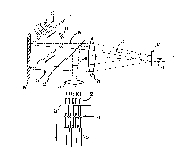
FIG. 1 illustrates the apparatuæ of the invention for
temporally-multiplexed optical pulse serial to parallel
converslon;
FIG. 2 illustrates the optical pulse parallel to
serial conversion apparatus and data multiplexing method
according to the present invention; and
FIG. 3 is a diagram of an input parallel data
pattern.
21~8~6~
DET~TT-T~n DESCRIPTION OF THE PREFERRED EMBODIMENTS
Referring now in specific detail to the drawings,
with like reference numerals identifying similar or
identical elements, as shown in FIG. 1, the present
disclosure describes all-optical serial-to-parallel and
parallel-to-serial conversion of ultrafast optical
signals. Ultrafast optical signal conversion is described
in commonly owned U.S. application Ser. No. 08/177,018,
filed January 4, 1994, entitled METHOD AND APPARATUS FOR
PROCESSING ULTRAFAST OPTICAL SIGNALS, and U.S. application
filed November 11, 1994, entitled METHOD AND APPARATUS FOR
PROCESSING ULTRAFAST OPTICAL SIGNALS, which are
incorporated herein by reference.
SERIAL-TO-P~T~'~TTT~'T C~O~v~iKSION
In FIG. 1, for serial-to-parallel conversion, the
apparatus receives a multiplexed signal 10 as a packet
having N bits. The signal 10 may be temporally
multiplexed real time optical pulse data, including
interleaved optical signals for N users transmitted in the
range of around 10 Gbits/sec to around 10 Tbit/sec. The
wavelength spectrum of this packet is holographically
recorded by interaction with an optical reference pulse in
a multiple quantum well (MQW) material 12 or other
holographic materials that can be dynamically written and
erased at the packet rate. Both the signal 10 and a
reference pulse 14 are diffracted by a dispersive element
16 which may be a diffraction grating, a Dragone router,
or any other dispersive element that has an output-angle
that varies as a function of input wavelength.
Preferably, the optical reference pulse 14 is
synchronized with the packet signal 10 by a locally-
regenerated data clock having one pulse per packet, which,
for example, may be generated by two stages of the clock
regeneration scheme described by K. Smith et al., "All-
- 21~8668
- 4 -
Optical Clock Recovery Using a Mode-Locked Laser",
ELECTRONICS LETT., VOL. 28, NO. 19, Sept. 1992, pp. 1814-
1816. A first stage provides a uniform pulse train at the
bit rate, and the second stage providing a divide-by-N
function, where N is the number of bits per packet. Both
the duration of the packet signal 10 as well as the time
delay between the packet signal 10 and reference pulse 14
may not exceed the time window given by the inverse of the
spectral resolution ~v of the grating 16.
The packet signal 10 and the reference signal 14 are
dispersed as beams 15, 17 by grating 16, pass through a
beam splitter 18 and are converted to a wavelength
spectrum signal by a Fourier lens 20. Such a Fourier lens
is a lens having a distance from an input plane and the
lens equal to the distance form the lens to the output
plane. The interference pattern between the spectrum of
the packet signal and the reference signal is recorded in
the holographic medium 12 located at the spectrum plane of
the Fourier lens 20.
Preferably, the hologram patterns produced by the
optical data packets stored in the MQW material 12 are
written and dynamically erased in synchronization with the
packet signals 10, so that interference fringes stored in
the MQW 12 decay within a time less than the temporal
delay between succeeding packets or are erased before the
next packet arrives. The erasure may be by flooding the
MQW 12 with light from a separate laser source (not
shown). In the present embodiment, the patterns are
overwritten. The MQW 12 is preferably made of GaAs or
InGaAs for operation around 800 nm or 1.5 ~m,
respectively. The hologram is read by a continuous-wave
(cw) laser projecting a beam 24 at around 800 nm or 1.5
~m, respectively. To read the MQW hologram 12, a cw beam
of light 24 illuminates the MQW 12 to produce a diffracted
beam 26. The diffracted beam 26 is Fourier transformed by
21~66~
- 5
the lens 20 and reflected by the beam splitter 18 to
introduce an image 22 at the output plane 23 of the lens
27. This image 22 displays the N bits of the multiplexed
signal 10 in parallel. The scaling between temporal and
spatial patterns is described by:
t - x A (1)
dc-cos~
where A is the wavelength of the laser, d is the pitch of
the grating used, c the speed of light, and ~ is the angle
at which the diffracted light beams 15, 17 emerge from the
diffraction grating 16. Extensions to different
read/write focal lengths and wavelengths may also be
performed.
The conversion of the N temporal input bits of the
multiplexed signal 10 into N output bits 22 formatted in
parallel at the output plane of the disclosed holographic
system and method provide for data rate reduction and
demultiplexing for ultrafast optical signals.
The optical bits 22 are output to respective channels
with each being converted to parallel beams in free space
by a microlens array 30 close to the ends of a bundled
optical fiber 32.
p~r.T.RT.-TO-SERIAL CONVERSION
FIG. 2 is a diagram of optical pulse parallel to
serial conversion and data multiplexing. The conversion
apparatus and method facilitates optically remultiplexing
of the signals switched to separate fibers in FIG. 1 for
serial transmission. Alternatively, the apparatus may
also be used to multiplex data from different users or
communication channels onto a single high bit-rate
communications channel.
In the exemplary embodiment of FIG. 2, electrical
signals produced from reduced-rate optical signals in a
21~g668
- 6 -
plurality of separate channels drive respective elements
in a field effect transistor self-electro-optic effect
device (FET-SEED) electro-absorption light modulator array
34. Electro-optic, acousto-optic, liquid crystal, or
mechanical modulator arrays may, alternatively, be used.
FET-SEED array elements are capable of modulation rates to
622 Mbits/sec in arrays of up to 128x128 elements, as
described in T.K. Woodward et al., "GaAs/AlGaAs FET-SEED
Receiver/Transmitters", OSA PROC. ON PHOTONICS IN
SWTICHING, VOL. 16, 1993, pp. 89-93. The FET-SEED
modulator array 34 is positioned at an input plane of a
first Fourier lens 36.
As shown in FIG. 2, a MQW holographic device 38 is
located at the spectral plane of that first Fourier lens
36. The modulator array 34 of the plurality of separate
channels and the MQW holographic device 38 is illumina~ed
by a beam of light 40 from a continuous-wave (cw) laser
42, such as a laser diode with a wavelength of 830 nm for
reading the pattern of the modulator array 34. The
modulator array 34 is shown as a transmission modulator.
Reflection modulators such as a FET-SEED array may also be
used.
As shown in FIG. 3, each pixel in a pattern 44 in the
modulator array 34 includes the data from each individual
channel to be multiplexed, with the exception of one pixel
46 on the modulator array 34 reserved as a reference pixel
and is not modulated. The interference fringe pattern
formed between the beam from the reference pixel 46 and
the data pixel pattern 44 is written into the MQW
holographic device 38, where it is dynamically written and
erased at a speed equal to the bit rate of the individual
channels of the modulator array 34.
Referring to FIG. 2, an optical pulse 48 is provided
by a laser (not shown), which may be a mode-locked laser
which may be made of Ti-Sapphire, Cr-LiSAF or
Z1~668
-- 7
Cr-LiCaF. In the exemplary embodiment, the operating
wavelength of around 850 nm is used if GaAs/AlGaAs quantum
well modulators are used or an Erbium-doped fiber laser
operating at 1. 5 ~m is used, synchronized to the bit rate
5 of the channels of the modulator array 34. In this
example, the duty cycle of the laser is less than the
inverse of N times the bit rate, where N is the number of
parallel channels of the modulator array 34.
Semiconductor solid-state or fiber lasers may also be
used.
The optical pulse 48 is directed to a first
reflective diffraction grating 50 having 600 lines/mm and
positioned at the input plane of the first Fourier lens 36
having the MQW holographic device 38 at its spectrum
15 plane.
The diffracted optical pulse 52 passes through a beam
splitter 54 and co-propagates with the modulator pattern
beams 56 illuminated from the modulator array 34 and
reflected by the beam splitter 54.
The beam 52 is diffracted at signal 58 from the
fringe patterns recorded in the MQW holographic device 38.
This diffracted signal 58 is then Fourier-transformed by a
second Fourier lens 60 and by a second diffraction grating
62 at the output plane of the second Fourier lens 60. The
25 serially-recombined signals 64 are then entered into a
single optical fiber 66 through an imaging lens 68 as
multiplexed data. The undiffracted beam 59 is discarded.
While the disclosed ultrafast serial-to-parallel and
parallel-to-serial conversion apparatus and method has
30 been particularly shown and described with reference to
the preferred embodiments, it will be understood by those
skilled in the art that various modifications in form and
detail may be made therein without departing from the
scope and spirit of the invention. Accordingly,
35 modifications such as those suggested above, but not
~lS8668
- - 8 -
limited thereto, are to be considered within the scope of
the invention.