Language selection

Search

Patent 2158722 Summary

Third-party information liability

Some of the information on this Web page has been provided by external sources. The Government of Canada is not responsible for the accuracy, reliability or currency of the information supplied by external sources. Users wishing to rely upon this information should consult directly with the source of the information. Content provided by external sources is not subject to official languages, privacy and accessibility requirements.

Claims and Abstract availability

Any discrepancies in the text and image of the Claims and Abstract are due to differing posting times. Text of the Claims and Abstract are posted:

  • At the time the application is open to public inspection;
  • At the time of issue of the patent (grant).
(12) Patent Application: (11) CA 2158722
(54) English Title: OPTICAL COUPLING ARRANGEMENT
(54) French Title: DISPOSITIF DE COUPLAGE OPTIQUE
Status: Deemed Abandoned and Beyond the Period of Reinstatement - Pending Response to Notice of Disregarded Communication
Bibliographic Data
(51) International Patent Classification (IPC):
  • G02B 06/30 (2006.01)
  • G02B 06/12 (2006.01)
  • G02B 06/26 (2006.01)
  • G02B 06/42 (2006.01)
  • G02F 01/313 (2006.01)
(72) Inventors :
  • HILDEBRAND, OLAF (Germany)
  • HOFFMANN, WALTER (Germany)
  • MAYER, HANS-PETER (Germany)
  • REHM, WERNER (Germany)
  • WUNSTEL, KLAUS (Germany)
(73) Owners :
  • ALCATEL N.V.
(71) Applicants :
  • ALCATEL N.V.
(74) Agent: ROBIC AGENCE PI S.E.C./ROBIC IP AGENCY LP
(74) Associate agent:
(45) Issued:
(22) Filed Date: 1995-09-20
(41) Open to Public Inspection: 1996-03-22
Examination requested: 2001-05-03
Availability of licence: N/A
Dedicated to the Public: N/A
(25) Language of filing: English

Patent Cooperation Treaty (PCT): No

(30) Application Priority Data:
Application No. Country/Territory Date
P 44 33 605.5 (Germany) 1994-09-21

Abstracts

English Abstract


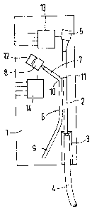
An optical duplexer, configured as a directional
coupler, is integrated into an optical coupling
arrangement with a fiber optic pigtail, constructed in
planar-optical hybrid technology on a substrate (1). To
reduce the required surface area and decrease optical
cross talk, the branch of the directional coupler
(waveguide 6, branch 7) is sharply bent. The bend is
equipped with a reflecting mirror (11) integrated
opposite the inner edge (10) of the bend. Furthermore,
the waveguiding end of the bent branch (7) is equipped
with a cylindrical lens. A laser diode (8) is located
before this, and a photodiode (5) is located before the
angled end of the straight-line integrated waveguide (2).


Claims

Note: Claims are shown in the official language in which they were submitted.


CLAIMS
1. An optical coupling arrangement with a first
optical waveguide (2) integrated on a substrate, and a
second branched optical waveguide (6) in parallel
thereto, characterized in that a branching portion of the
second optical waveguide (6) is bent into a bend (10) and
equipped with a reflecting mirror (11) opposite an edge
of the bend (10).
2. An optical coupling arrangement as claimed in
claim 1, characterized in that it is constructed as a
transceiver with a duplexer on the substrate (1).
3. An optical coupling arrangement as claimed in
claim 1, characterized in that ends of the first optical
waveguide (2) are coupled to a photodiode (5) and to a
fiber optic pigtail (4) affixed to a groove (3) in the
substrate (1), and one end of the second optical
waveguide (6) is coupled to a laser diode (8).
4. An optical coupling arrangement as claimed in
claim 3, characterized in that an end of a bent branch
(7) of the branching portion of the second optical
waveguide is equipped with a cylindrical lens, and that
the laser diode (8) is located before the cylindrical
lens.
5. An optical coupling arrangement as claimed in
claim 4, characterized in that a free end (9) of the
second optical waveguide (6) is built as a sump to
suppress reflections.
6. An optical coupling arrangement as claimed in
claim 3, characterized in that an end of the first
optical waveguide (2) to which the photodiode (5) is
coupled, is angled to prevent backward reflections.

7. An optical coupling arrangement as claimed in
claim 3, characterized in that another optical waveguide
is coupled to the first optical waveguide (2), having a
free end that leads into a sump and that decouples and
suppresses portions of signals in the first optical
waveguide that originate from the laser diode (8), which
are reflected in a direction toward the photodiode (5).
8. An optical coupling arrangement as claimed in
claim 7, characterized in that coupling areas formed by
the first optical waveguide (2), the second optical
waveguide (6) and the other optical waveguide, which
represent directional couplers, are provided so that the
middle frequencies of suppressed band areas thereof are
displaced with respect to each other.
9. An optical coupling arrangement as claimed in
claim 2, characterized in that ends of the first optical
waveguide (2) are coupled to a photodiode (5) and to a
fiber optic pigtail (4) affixed to a groove (3) in the
substrate (1), and one end of the second optical
waveguide (6) is coupled to a laser diode (8).
10. An optical coupling arrangement as claimed in
claim 4, characterized in that an end of the first
optical waveguide (2) to which the photodiode (5) is
coupled, is angled to prevent backward reflections.
11. An optical coupling arrangement as claimed in
claim 5, characterized in that an end of the first
optical waveguide (2) to which the photodiode (5) is
coupled, is angled to prevent backward reflections.
12. An optical coupling arrangement as claimed in
claim 4, characterized in that another optical waveguide
is coupled to the first optical waveguide (2), having a
free end that leads into a sump and that decouples and

suppresses portions of signals in the first optical
waveguide that originate from the laser diode (8), which
are reflected in a direction toward the photodiode (5).
13. An optical coupling arrangement as claimed in
claim 5, characterized in that another optical waveguide
is coupled to the first optical waveguide (2), having a
free end that leads into a sump and that decouples and
suppresses portions of signals in the first optical
waveguide that originate from the laser diode (8), which
are reflected in a direction toward the photodiode (5).
14. An optical coupling arrangement as claimed in
claim 6, characterized in that another optical waveguide
is coupled to the first optical waveguide (2), having a
free end that leads into a sump and that decouples and
suppresses portions of signals in the first optical
waveguide that originate from the laser diode (8), which
are reflected in a direction toward the photodiode (5).

Description

Note: Descriptions are shown in the official language in which they were submitted.


2158722
OPTICAL COUPLING ARRANGEMENT
Technical Field
The invention relates to an optical coupling
arrangement for use in optical communication systems.
Backqround of the Invention
A configuration example of an optical duplexer is
known from DE 42 30 952 A1, in which a silicon substrate
equipped with integrated optical functional units is
affixed in a housing, among others. The silicon
substrate supports a beam splitter, which is integrated
in the form of optical line paths and acts as a
directionally selective wavelength coupler. A
semiconductor laser diode is coupled before one end of a
first straight line path, and a fiber optic pigtail is
coupled to the other end of this line path. A second
optical line path, which is coupled to the first line
path by a cut that runs parallel to it, ends in a bent
cut before a photodiode which is affixed to the silicon
substrate.
Disclosure of Invention
The invention has the task of reducing a substrate
surface required for an optical coupling arrangement with
a first optical waveguide integrated on the substrate,
and a second branched optical waveguide in parallel
thereto, and to improve its performance. The invention
fulfills this task with a branching portion of the second
optical waveguide being bent and equipped with a
reflecting mirror opposite an edge of the bend.
According further to the invention, the coupling
arrangement is constructed as a transceiver with a
duplexer on the substrate.
In further accord with the invention, the ends of
the first optical waveguide are coupled to a photodiode
and to a fiber optic pigtail affixed to a groove in the
substrate, and one end of the second optical waveguide is
coupled to a laser diode. The end of the bent branch may

21 ~8 722
be equipped with a cylindrical lens, and the laser diode
may be located before the cylindrical lens. Moreover, a
free end of the second optical waveguide may be built as
a sump to suppress reflections, and the end of the first
optical waveguide, on which the photodiode is located,
can be angled to prevent backward reflections.
Furthermore, another optical waveguide may be coupled to
the first optical waveguide, whose free end leads into
the sump and decouples and suppresses portions of signals
in the first optical waveguide that originate from the
laser diode, which are reflected in the direction of the
photodiode. The coupling areas formed by the first
optical waveguide, the second optical waveguide and the
other optical waveguide, which represent directional
couplers, may be designed so that the middle frequencies
of their suppressed band areas are provided slightly
displaced with respect to each other.
These and other objects, features and advantages of
the present invention will become more apparent in light
of the detailed description of a best mode embodiment
thereof, as illustrated in the accompanying drawing.
Brief Description of the Drawinq
The sole figure shows a configuration example of an
optical coupler according to the invention, illustrated
ln a top view.
Best Mode for Carryinq Out the Invention
In the figure, the reference numeral 1 denotes a
rectangular substrate. The substrate 1, which is made of
silicon or quartz for example, supports a first optical
waveguide 2 made of sio2, which runs parallel and in a
straight line at a specified distance from one lengthwise
edge. Before one of its ends, a fiber optic pigtail 4 is
located in a groove 3 with a V-shaped cross section, and
a semiconductor photodiode 5 is located at the other end
of this waveguide 2. The end of the waveguide which

2158722
faces the photodiode 5 is at an angle to prevent backward
reflections.
A second optical waveguide 6 made of sio2, which is
integrated into the substrate 1 and is coupled to the
first waveguide 2 with a parallel running cut, ends in a
bent branch 7 before a semiconductor laser diode 8. The
other free end of this waveguide 6, which contains a bend
with a relatively large radius, is configured as a sump
to suppress potential reflections.
To ensure small insertion losses, the necessary
branching of both waveguides 2, 6 should take place with
as little bending as possible. However, this requires a
relatively large space on the substrate. To better
utilize the substrate surface and the required space, a
sharp bend is provided in the branch 7 of the second
optical waveguide 6 facing the laser diode 8, in the
coupling area which runs parallel to the first optical
waveguide 2, and the sharply contoured bend is equipped
with a reflecting mirror 11 which is integrated opposite
the inner edge 10 of the bend. Directly at the end of
the coupling area, or shortly after the bend, i.e. an
area in which the waveguides 2, 7 are already optically
separated from each other, the reflecting mirror 11,
which can be manufactured with dry etching technology,
permits arranging the branch 7 of the second optical
waveguide 6, which leads to the laser diode 8, at an
angle of 45 with respect to the first optical waveguide
2. To improve the coupling efficiency of the laser diode
8, the waveguiding end of this branch 7 is equipped with
a cylindrical lens, which can be manufactured with the
same etching technology as the reflecting mirror 11.
The branch 7, which is sharply bent from the
coupling waveguiding area, permits the installation of an
amplifier circuit 13 on the substrate surface between the
laser diode 8, which is potentially coupled to an
integrated monitor diode 12, and the photodiode 5. The
drive electronics 14 for the laser and monitor diodes 8,

21~8722
12 can be located under the laser diode 8, in the area
next to the coupling area of the second optical waveguide
6.
The planar-optically constructed transceiver, with
the optical duplexer indicated in the drawing as a
directional coupler, can be cost-effectively manufactured
in a monolithic configuration with hybrid technology and
using other suitable substrate materials, and imbedded in
plastic to protect it against effects of the environment,
depending on the number of pieces required. In addition,
the widely spaced placement of photodiode 5 and laser
diode 8 strongly reduces electrical cross talk.
To filter out portions of the signal emitted by the
laser diode 8, which are reflected in disturbance areas
in the first optical waveguide 2, and in the receiving
direction of the fiber optic pigtail 4 which follows the
transmission direction, and disrupt the reception by the
photodiode, another optical waveguide (not illustrated in
the figure) can be coupled to the first optical waveguide
between the bend of the second optical waveguide and the
end of the first optical waveguide, which is coupled to
the photodiode. Like the second optical waveguide, it is
integrated on the substrate where it is bent and leads to
a sump along a coupling area which is parallel to the
first optical waveguide and runs in the direction of the
photodiode.
If the coupling areas formed by the first optical
waveguide and the other two optical waveguides are
designed so that the middle frequencies of the suppressed
band areas in the resulting directional couplers are
slightly displaced with respect to each other, a larger
width of the suppressed band areas can be achieved, and
thereby better decoupling of the sending and receiving
branches.
Although the invention has been shown and described
with respect to a best mode embodiment thereof, it should
be understood by those skilled in the art that the

.- 21 S8 722
foregoing and various other changes, omissions and
additions in the form and detail thereof may be made
therein without departing from the spirit and scope of
the invention.

Representative Drawing
A single figure which represents the drawing illustrating the invention.
Administrative Status

2024-08-01:As part of the Next Generation Patents (NGP) transition, the Canadian Patents Database (CPD) now contains a more detailed Event History, which replicates the Event Log of our new back-office solution.

Please note that "Inactive:" events refers to events no longer in use in our new back-office solution.

For a clearer understanding of the status of the application/patent presented on this page, the site Disclaimer , as well as the definitions for Patent , Event History , Maintenance Fee  and Payment History  should be consulted.

Event History

Description Date
Inactive: IPC from MCD 2006-03-11
Application Not Reinstated by Deadline 2003-07-11
Inactive: Dead - Final fee not paid 2003-07-11
Deemed Abandoned - Failure to Respond to Maintenance Fee Notice 2002-09-20
Deemed Abandoned - Conditions for Grant Determined Not Compliant 2002-07-11
Notice of Allowance is Issued 2002-01-11
Letter Sent 2002-01-11
Inactive: Approved for allowance (AFA) 2001-12-27
Letter Sent 2001-06-21
Inactive: Status info is complete as of Log entry date 2001-06-19
Inactive: Application prosecuted on TS as of Log entry date 2001-06-19
Amendment Received - Voluntary Amendment 2001-05-15
All Requirements for Examination Determined Compliant 2001-05-03
Request for Examination Requirements Determined Compliant 2001-05-03
Application Published (Open to Public Inspection) 1996-03-22

Abandonment History

Abandonment Date Reason Reinstatement Date
2002-09-20
2002-07-11

Maintenance Fee

The last payment was received on 2001-08-29

Note : If the full payment has not been received on or before the date indicated, a further fee may be required which may be one of the following

  • the reinstatement fee;
  • the late payment fee; or
  • additional fee to reverse deemed expiry.

Patent fees are adjusted on the 1st of January every year. The amounts above are the current amounts if received by December 31 of the current year.
Please refer to the CIPO Patent Fees web page to see all current fee amounts.

Fee History

Fee Type Anniversary Year Due Date Paid Date
MF (application, 2nd anniv.) - standard 02 1997-09-22 1997-08-22
MF (application, 3rd anniv.) - standard 03 1998-09-21 1998-08-18
MF (application, 4th anniv.) - standard 04 1999-09-20 1999-08-23
MF (application, 5th anniv.) - standard 05 2000-09-20 2000-08-24
Request for examination - standard 2001-05-03
MF (application, 6th anniv.) - standard 06 2001-09-20 2001-08-29
Owners on Record

Note: Records showing the ownership history in alphabetical order.

Current Owners on Record
ALCATEL N.V.
Past Owners on Record
HANS-PETER MAYER
KLAUS WUNSTEL
OLAF HILDEBRAND
WALTER HOFFMANN
WERNER REHM
Past Owners that do not appear in the "Owners on Record" listing will appear in other documentation within the application.
Documents

To view selected files, please enter reCAPTCHA code :


To view images, click a link in the Document Description column. To download the documents, select one or more checkboxes in the first column and then click the "Download Selected in PDF format (Zip Archive)" or the "Download Selected as Single PDF" button.

List of published and non-published patent-specific documents on the CPD .

If you have any difficulty accessing content, you can call the Client Service Centre at 1-866-997-1936 or send them an e-mail at CIPO Client Service Centre.


Document
Description 
Date
(yyyy-mm-dd) 
Number of pages   Size of Image (KB) 
Representative drawing 1998-02-16 1 7
Representative drawing 2001-12-27 1 5
Description 1996-03-21 5 202
Abstract 1996-03-21 1 20
Claims 1996-03-21 3 107
Description 2001-05-14 13 594
Claims 2001-05-14 8 378
Drawings 1996-03-21 1 10
Acknowledgement of Request for Examination 2001-06-20 1 179
Commissioner's Notice - Application Found Allowable 2002-01-10 1 164
Courtesy - Abandonment Letter (NOA) 2002-09-18 1 170
Courtesy - Abandonment Letter (Maintenance Fee) 2002-10-20 1 179
Correspondence 1995-12-19 2 49