Note: Descriptions are shown in the official language in which they were submitted.
2159399
~,
DOPP~ER RADAR DETECTION SYSTEM
BACKGROUND OF THE INVENTION
This invention relates to methods of and circuits for
suppressing radar output due to clutter and noise while retaining
desired output due to targets that are moving with velocities
different than those of clutter. The invention is applicable to
radars that operate on the doppler principle of detection and
therefore it is applicable to cw doppler, pulse doppler and MTI
(moving target indication) radars.
The principles of the three aforementioned types of radars
are given in Chaps. 3 and 4 of the book Introduction of Radar
Systems, McGraw-Hill Book Company, 1980, by M. I. Skolnik.
Throughout this document the term "doppler radar" refers to either
MTI, cw or pulse doppler radar.
This disclosure relates to the detection of moving targets
with doppler radar for which the target echoes have relatively
high doppler frequencies, and the rejection of land and sea
clutter and noise. Radar clutter signals are unwanted signals
caused by radar echo (see, e.g., Skolnik, p. 470), and clutter
signal magnitude therefore depends on radar range and direction.
Land and sea clutter, being from stationary and slowly moving
objects, have relatively small doppler frequencies including
frequencies at and near zero. Noise signals, on the other hand,
are unwanted signals caused by random fluctuations having wide
doppler frequency spectra extending from zero to an upper limit
2159399
.,_
controlled by receiver bandwidth (Skolnik, pp. 23-29). Unli~ke
clutter echo, noise at the radar output occurs at all radar
ranges.
Based on the relative strengths of the doppler frequency
components contained in the radar echo, doppler processors use
filters to suppress signals from clutter and to retain signals
from moving targets. These filters can be implemented in analog
or digital hardware, or in software. Ideally the output of a
doppler radar due to clutter is zero. However, a radar has
frequency and amplitude instabilities that cause its doppler
processed output to fluctuate, even though the echo is from a
stationary object. Another cause for fluctuations in echo
strength, which provides another source of non-zero doppler
frequencies, is beam movement across a reflecting object due to
antenna sc~nn;ng. Therefore, radar output after doppler
processing caused by stationary objects (clutter) is oftentimes
much stronger than the output caused by some (the weaker) moving
targets of interest.
The usual technique for rejecting clutter and noise is to
employ an amplitude threshold level below which signals are
rejected. Unfortunately, the threshold rejects the weaker targets
and passes the stronger clutter and therefore amplitude
thresholding is satisfactory only if, at the output of the doppler
processor, the important target signals are stronger than most of
the clutter and noise.
Modern automatic detection radars use a thresholding circuit
2I59399
"~
called CFAR (constant false alarm ratio). The CFAR operates~by
adaptively following interference (whether from receiver or
external noise or from clutter) and adjusting the threshold level
so as to automatically reject the interference in each range cell
(Skolnik, pp. 392-395). CFAR performance is effective against
homogeneous clutter and noise. However, CFARs are inefficient
suppressors of typical surface (ground and/or sea) clutter, which
is not homogeneous and often consists of isolated and very strong
clutter areas interspersed with regions of negligible clutter.
The most commonly used CFAR is called a range CFAR. A range
CFAR sets its threshold in each range cell based on sampling,
during each range sweep, the strengths of signals in its
neighboring cells. Next it combines and obtains a statistic
(usually an average) of the sampled signals, and it sets a
threshold for said each range cell. Then for each range cell, a
radar signal is outputted if it exceeds its threshold. Thus, a
detection is declared at a given range cell if it contains a
signal that exceeds its threshold based on its aggregate of
signals from nearby cells. Another well known type of CFAR is
called a doppler CFAR. It samples doppler cells (filters), which
are numerous in some pulse doppler radars (see, e.g., Patton and
Ringel, U.S. Patent 3,701,149). Then, based on a sampling of
doppler cells, a threshold is set for each range cell.
Modern radars have a large number of range cells, and
therefore CFAR processing is complex. In addition, a common
weakness of CFARs is lack of robustness, i.e., inability to
2159399
....
._
process effectively a wide variety of clutter types. Various
trade-offs in CFAR designs can be made to accommodate problems of
detection efficiency and false alarms that are created by both (1)
a wide variety of clutter types and (2) the presence of multiple,
closely spaced targets within nearby range cells (see, e.g., G.V.
Morris, Airborne Pulse Doppler Radar, Artech House, 1988, Chapter
17). However, the changes in design required for solving these
problems contribute to additional complexity; and thus contibute
to further increases in size, weight and costs.
U.S. Patents 4,459,592 and 4,684,950 teach ratio comparator
methods and means for establishing an adaptive clutter threshold
level to reject isolated clutter even though it is very strong.
More specifically, a ratio comparator technique is taught that
functions on the basis of the ratio of the amplitudes of two
signals: one proportional to the radar received signal and which
contains doppler frequencies at and near zero_and the other
proportional to the output of the doppler processor.
U.S. Patent 4,684,950 teaches additional clutter thresholding
that cooperatively operates with the basic ratio comparator
technique for improving clutter suppression if the suppression is
impaired by a limited receiver amplitude dynamic range or by
clutter fluctuations caused, e.g., by wind blown trees. The
additional thresholding of U.S. Patent 4,684,950 functions
specifically on the amplitude of the radar received signal prior
to doppler processing, in relation to at least one fixed amplitude
level. On the other hand, the present disclosure teaches a noise
215939~
.~",
". .....
thresholder employed after doppler processing in operative~
association with the above-mentioned ratio comparator technique.
In this combination, the new invention suppresses both the clutter
and noise at the radar output over the full range of clutter and
noise mixes, from clutter with imperceptible noise to noise with
imperceptible clutter.
U.S. Patents 4,459,592 and 4,684,950 teach the use of a CFAR
in combination with the ratio comparator technique to provide
improved target detection and clutter suppression performance over
that attainable with only a CFAR. As discussed later in this
disclosure, the present invention has a number of advantages over
the ratio comparator/CFAR combination previously taught, including
less complexity and greater sensitivity for detecting targets in
land and sea clutter.
SUMMARY OF THE lNV~;N'l'lON
It is known from radar experiments and computer simulations,
that the ratio comparator technique originally taught in U.S.
Patent 4,459,592 provides excellent performance for rejecting
ground clutter if, at the output of the doppler processor, the
clutter is strong relative to noise. However, its performance for
rejecting clutter depends in an inverse manner on the ratio of
clutter power to noise power. In other words, the capability of
the ratio detector for suppressing a mixture of noise and clutter
depends on the clutter to noise ratio, ranging from excellent for
the large clutter-to-noise ratios to completely ineffective for
noise only. Explanations are given under Detailed Description of
l_ 2159399
._
the Preferred Embodiments on why the clutter suppression .
capability of the ratio comparator technique increasingly
decreases for smaller values of clutter relative to noise; and how
the present invention improves the target detection and clutter
suppression capabilities of doppler radars.
The present invention employs a noise thresholder that
functions in operative association with the ratio comparator
technique. The noise thresholder is operated to reject noise
without clutter, and it is therefore ineffective for suppressing
noise plus clutter. Similarly, the clutter thresholder (which
employs the basic ratio comparator technique) rejects clutter only
when it is large compared to noise, and it is ineffective for
small clutter-to-noise ratios. By functioning in operative
association, the combined thresholders provide a doppler detection
system which, for a given false alarm rate due to noise and
clutter, permits the reliable detection of weaker targets than
would otherwise be possible. Furthermore, these improvements can
be obtained by avoiding the inherent complexities of range or
doppler CFARs.
To understand how the thresholding and logic circuitry
effects on the signals after being outputted from a doppler
processor, the reader should recognize the following:
(1) The amplitude differences between the signals from land
and/or sea clutter from adjacent and closely spaced range
cells can be very large.
(2) The clutter from a range cell, after being-outputted from
2159399
. ....
a doppler processor, is noise-like and fluctuates~between
successively received pulses because of imperfections in
clutter suppression and the presence of noise.
Thus, to reject both clutter and noise and yet efficiently detect
targets; the system (a) must establish a threshold at each range
cell which is independent of the clutter in its neighboring range
cells; (b) must adaptively adjust the clutter reject/target detect
threshold level in each range cell based on the level of land
and/or sea clutter in each said range cell for maximizing target
detection versus false alarm rate; and (c) must for the range
cells without clutter, for maximizing target detection capability,
provide a threshold level which is large enough to reject noise to
within a desired false alarm rate.
Two threshold levels are used for the system to accomplish
the above tasks, as follows:
-a noise threshold level which is established by a reference
voltage and has sufficient amplitude above the average noise
within the doppler processor output signal, at a given range cell,
to obtain a low false alarm rate in the absence of clutter; and
-a clutter threshold level which is established at each radar
range cell by attenuating a signal with magnitude in response to
the magnitude of the received signal and which contains doppler
frequencies at and near zero, at said each radar range cell.
The thresholding and logic of the radar detection system
effects on the basis of two independent, binary decisions: one
within the noise thresholder as to whether or not the magnitude of
~ 2159399
-
'!I_
a doppler processed signal exceeds the noise threshold levél; and
the other within the clutter thresholder as to whether or not the
doppler processed signal exceeds the clutter threshold level.
Each of the two binary decisions must be true for there to be
radar output, indicating target detection; otherwise the output is
rejected, indicating the presence of noise or clutter.
As is illustrated by the preferred embodiments of this
disclosure, the thresholding is done in each range/azimuth cell if
the doppler processor has only one doppler filter, such as a MTI
canceler or a bandpass filter. However, if the processor employs
a plurality of bandpass filters, the thresholding can be
accomplished in each range/azimuth/doppler cell.
The noise thresholder in operative association with the
clutter thresholder serves in several important ways: it provides
the thresholding needed for noise rejection in the absence of
clutter, it allows the clutter thresholder to reject clutter which
is large relative to noise, and it rejects the sum of clutter and
noise at any time it is smaller than the noise threshold. The last
item is of great importance because (a) it relieves the clutter
thresholder of the requirement to reject clutter for the smaller
clutter-to-noise ratios, when its clutter suppression capability
is ineffective; and (b) this allows a clutter threshold ratio to
be selected that permits the detection of smaller target signals
relative to clutter than would otherwise be possible.
It is of interest that if operating alone, the noise
thresholder would be ineffective for rejecting clutter, and the
2159~99
.......
clutter thresholder would be ineffective for rejecting clutter
except if large compared to noise. However, as a consequence of
being in operative association, both the noise thresholder
reference voltage and the clutter thresholder ratio can be
selected to provide a highly sensitive method for detecting target
signals that are in the presence of both noise and clutter.
As noted under Background of the Invention, U.S. Patent
4,684,950 teaches clutter thresholding with the basic ratio
comparator technique described above in combination with a
thresholder that compares the amplitude of the radar received
signal (prior to doppler processing) relative to a fixed amplitude
level. On the contrary, the present invention employs the
aforementioned noise thresholder and it functions on the basis of
the amplitude of signals after being doppler processed. Its
effect, therefore, is entirely different than the amplitude
thresholding taught in U.S. Patent 4,684,950. As already noted,
in that patent the amplitude thresholding compares the radar
received signal prior to doppler processing with a reference
level, because its purpose is to regulate on the basis of the
input clutter amplitude; not on the basis of the doppler processed
clutter amplitude relative to noise at the doppler processor
output, as is the case for the present invention.
The present invention has a number of advantages over the
ratio comparator/CFAR combination previously taught in U.S.
Patents 4,459,592 and 4,684,950, including less complexity and
greater sensitivity for detecting targets in land and/or sea
~ ~ 5 ~ 3 ~ 9 L
clutter. For example, CFAR circuit complexities are incurred to
accommodate the lack of robustness for a wide range of land and
sea clutter types (see e.g. G.V. Morris, Airborne Pulse Doppler
Radar, Artech House, 1988, Chapter 17). Such added complexities
are unnecessary in the present invention, because of its
inherent noise plus land and/or sea rejection capabilities.
Another CFAR loss which the present invention avoids is caused
by the CFAR threshold being raised in amplitude by land and/or
sea clutter in the range or doppler cells that are sampled for
establishing a CFAR threshold. This loss can be avoided with
the present invention by establishing a reference voltage level
for the noise thresholder at a range where land and/or sea
clutter is negligible. Avoided also is the effect on range
CFARs of multiple, closely-spaced targets raising the CFAR
threshold level that reduces the sensitivity for detecting an
individual target.
Accordingly the present invention seeks to provide circuits
and methods that:
(1) Will adaptively adjust clutter-plus-noise reject/
target detect threshold levels for each radar range cell based
on the level of noise and land and/or sea clutter in each said
range cell for maximizing the target detection sensitivity
versus false alarm rate.
(2) Will improve the sensitivity of doppler radar for de-
tecting moving targets in the presence of clutter and noise over
the performance possible when operating with the doppler ratio
detection technique in combination with CFAR circuitry as taught
?
~ 21S939~
~..,
in U.S. Patents 4,459,592 and 4,684,950.
(3) Will provide a method for the automatic detection of
targets in the presence of clutter and noise that does not
require the use of either a range or a doppler CFAR; thereby
avoiding their inherent complexities and their lesser capabilities
for target detection in a land and/or sea clutter environment.
(4) Will provide a doppler radar detection system that
employs both a clutter and a noise thresholder, and a noise
thresholder reference voltage level of fixed amplitude.
(5) Will provide a doppler radar detection system that
employs both a clutter and a noise thresholder, and a noise
thresholder reference voltage level that adaptively responds to
changes in internally generated receiver noise plus noise from
external sources.
(6) Will provide a doppler radar detection system that
employs threshold levels at a plurality of range cells or
range/azimuth areas for rejecting fast moving clutter.
(7) Can be used with MTI and pulse doppler radars which use
MTI (delay-line) cancelers that process either unipolar video,
bipolar video (either single signal or I and Q signals), IF or RF
signals.
(8) Can be used with cw doppler radar that uses a bandpass
doppler filter or a plurality of bandpass doppler filters.
(9) Can be used with a pulse doppler or a MTI radar which
uses a bandpass doppler filter or a plurality of bandpass doppler
filters.
' .,i~l~
(10) Can be used with a pulse doppler or an MTI radar which
uses an MTI (delay-line) canceller and a doppler bandpass filter
or an MT1 (delay-line) canceller and a plurality of bandpass
filters.
To accomplish these aspects, the subject invention
regulates signals that are doppler processed in a manner that
permits them to become clutter and noise suppressed radar
output. This is done through use of separate threshold levels:
one for rejecting the noise which is established with a
reference voltage that exceeds noise and the other for rejecting
clutter which is established by a ratio of the magnitudes of two
signals with different doppler frequency components. Then, if
both threshold levels are exceeded, the doppler processed signal
is declared a target; otherwise, it is rejected as being due
either to clutter and/or noise. The resultant effect is to
provide a doppler detection system which, for a given false
alarm rate due to land and/or sea clutter, permits the reliable
detection of weaker target signals than would otherwise be
possible. Furthermore, this enhanced detection performance can
be accomplished without the use of either a range or a doppler
CFAR; thereby avoiding their inherent complexities and their
lesser capabilities for target detection and land and/or sea
clutter rejection.
The invention in one aspect provides a radar detection
system for processing the received signal from a radar receiver
to detect moving targets while suppressing clutter and noise,
the clutter being radar echo signals from stationary and slowly
moving objects of land or sea having small doppler frequencies
,~
2~593~
", ~
.;,,~
including frequencies at and near zero and the noise being
randomly fluctuating signals having wide doppler spectra
including zero frequency. The system comprises doppler
processor means for frequency filtering the received signal and
providing at least one filtered signal in response to the
received signal, means of providing a first signal having
doppler frequencies at and near zero frequency with magnitude in
response to the magnitude of the received signal, means of
providing a second signal with a magnitude in response to the
magnitude of a filtered signal of the at least one filtered
signal and clutter thresholder means for comparing the first and
second signals and for providing a clutter thresholder output
signal of a first level only when the ratio of the second signal
magnitude to the first signal magnitude is less than a
predetermined value and of a second level whenever this ratio
exceeds the predetermined value. There is reference voltage
means for providing a reference voltage with magnitude that
exceeds the noise level of the second signal, noise thresholder
means for comparing the second signal magnitude and magnitude of
the reference voltage for providing a noise thresholder output
signal of a first level only when the second signal magnitude is
less than the magnitude of the reference voltage and of a
second level whenever the second signal magnitude exceeds the
magnitude of the reference voltage and radar output means for
selectively passing a radar output signal constituting a clutter
and noise suppressed radar output only in the presence of both
the clutter thresholder output signal and the noise thresholder
output signal being of the second level.
The invention also comprehends a method of doppler radar
12A
~ 7 ~
~,
",
detection of moving targets and for suppressing clutter and
noise through use of the systems.
DESCRIPTION OF THE DRAWINGS
FIG. 1 is a block diagram that illustrates the principal
features of an exemplary embodiment of the radar processing
system in accordance with the present invention.
12B
2159399
FIG. 2 is an alternate block diagram for the thresholding and
logic circuitry, block 100.
FIG. 3 is a block diagram that illustrates use of the basic
radar detection system invention in operative association with a
MTI canceler.
FIG. 4 is a block diagram that illustrates use of the basic
radar detection system invention in operative association with a
two-channel MTI canceler.
FIG. 5 is a block diagram that illustrates use of the basic
radar detection system invention in operative association with a
two-channel doppler filter bank cascaded with a two-channel MTI
canceler.
FIG. 6 is a block diagram that illustrates means for
generating a reference voltage that periodically samples in time.
FIG. 7 is a block diagram that illustrates means for
generating a reference voltage that samples different radar range
cells.
FIG. 8 is a block diagram that illustrates means for
generating a reference voltage that samples different bandpass
filters.
DETAILED DESCRIPTION OF THE PREFERRED EMBODIMENTS
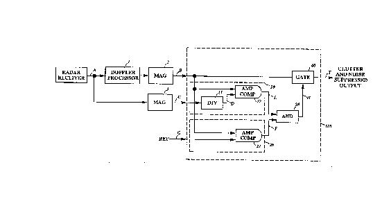
FIG. 1 illustrates the principal features of the invention. A
doppler radar receiver provides received signal A which is
filtered by doppler processor 1 and processed by magnitude
detector 2 to provide a doppler filtered unipolar signal B in
response to received signal A. Signal B along with signal C and
~- 2159~99
reference voltage G are supplied as input to block lOo. Block loo
contains thresholding and logic circuitry that: (1) if siqnal B is
due principally to a target, it is gated on to pass as output
signal T; but (2) if signal B is dominated by noise and/or
clutter, it is gated off and signal T is rejected for not being
due to a target. It is to be recognized that block 100 is
continuously responding to signal A via its inputs: signal B,
signal C, and reference voltage G. Thus, for a pulse radar,
signal A varies with time corresponding to radar range. Then, the
processing by block 100 is accomplished by making separate
thresholding and logic decisions for each radar range cell.
Now described is the method by which the thresholding and
logic circuitry, block 100, effects. Block 100 comprises two
thresholders that function in operative association: block 10 is
for clutter and is called a clutter thresholder, and block 20 is
for noise and is called a noise thresholder. It is subsequently
explained how the logic of block 100 causes blocks 10 and 20 to
function in operative association, so as to effectively output
target signals yet reject both clutter and noise in a mixed
noise/clutter/target environment.
As noted from FIG. 1, signal A is processed via two channels:
the one that contains signal B and another, wherein signal A is
input to magnitude detector 3 that provides unipolar signal C. It
is to be noted that (1) signal C is proportional to the magnitude
of signal A, and (2) signal B is responsive to the magnitude of
signal A because it is obtained after being doppler filtered by
2159399
,,~
doppler processor 1. A doppler processor operates as follows:
1. For a stationary reflecting object, it causes the strength
of signal B to be much less than signal A or signal C. Therefore,
for a stationary object the ratio of the strengths of signal B to
signal C is very small; and
2. For a moving target, the relative strength of signals B
and C depends on target velocity, but the ratio of the strengths
of signal B to signal C is rarely as small as that ratio for a
stationary object.
The clutter thresholder, block 10, is a ratio comparator that
follows the teachings of U.S. Patents 4,459,592 and 4,684,950.
It continuously compares signals C and B within each radar range
cell and provides a clutter thresholder output signal E only when
the ratio of signal B to signal C exceeds a predetermined ratio.
This predetermined ratio is established by the attenuation of
signal C caused by the divider, ~lock 11, which results in the
creation of signal D. Specifically, signal E is output from
comparator 12 if signal B exceeds signal D, where signal D is
obtained by attenuating signal C with divider 11.
The noise thresholder, block 20, comprises amplitude
comparator 21 to which signal B and a reference voltage G are
input. By this means, signal F is output from amplitude comparator
21 if signal B exceeds reference voltage G. When signal B is
dominated by noise, signals B and D fluctuate independently of one
another. Then, however, signal B is almost always larger than
signal D because (1) of the attenuation of divider 11 and (2)
2I59399
"~ .
noise, if suppressed, is not strongly suppressed by a doppler
processor. Then, for practical purposes the clutter thresholder
output E from block lo is almost always present. Therefore, when
the noise in signal B exceeds reference voltage G so that signal F
is created at the output of amplitude comparator 21, the almost
certain simultaneous presence of signals E and F at AND gate 30
will create signal H with high probability. Thus, the existence of
signal H due to noise is then propagated via gate 40, which passes
signal B so as to become a noise false alarm at the radar output,
signal T. Therefore, when signal B is dominated by noise (and
thus thresholder output E is almost always present), to maintain a
given low false alarm rate due to noise at the radar output
(signal T), it is necessary that the level of reference voltage G
exceeds the average noise level of signal B by an amount
sufficient to maintain a low false alarm rate for signal F.
Reference voltage G serves three important roles, the first
is described immediately above. Namely, it directly limits the
generation of false alarms in signals F and H when signal B is
dominated by noise. The second role is to reduce the false alarm
rate of signal H caused by the combination of noise and clutter
within signal B, because then signals E and F are generally not
present simultaneously. For this condition, signal H (which
requires the simultaneous presence of signals E and F) has a false
alarm rate that is considerably less than the false alarm rates of
either signal E or signal F.
The third role of reference voltage G is to provide a level
16
2159399
, ..
~,
below which the sum of clutter and noise is rejected. This role
provides much power to the present invention because (a) it
relieves the clutter thresholder of the requirement to reject
clutter for the smaller clutter-to-noise ratios, when its clutter
suppression capability is ineffective; and (b), as will now be
addressed, it allows a clutter threshold ratio to be selected that
permits the detection of smaller target signals relative to
clutter than would otherwise be possible.
The following should be noted: (1) An increase in the
attenuation caused by divider 11 decreases the amplitude of signal
D. (2) This reduction of signal D permits a smaller target signal
to clutter-plus-noise ratio of signal B to generate signal E. (3)
This reduction of signal D causes an increase in the false alarm
rate of signal E, because signal B fluctuates rapidly (pulse-to-
pulse) due to clutter and noise. (4) For proper operation,
reference voltage G is relatively large compared to the average
receiver noise and therefore signal F is generated only when
signal B is relatively large compared to average noise. Thus, (5)
signal H and radar output signal T are generated in presence of a
target for which signal B exceeds both signal D and reference
voltage G. Furthermore, (6) the generation of signal F (as well
as signals H and T) is prohibited when signal B is less than
reference G. (7) The prohibition of signal H rejects the false
alarms that would otherwise be caused by signal E, which occur
because of large signal B to signal D ratios (in absence of
target) that exist when the clutter-to-noise ratio of signal B is
21~939~
.,." i
relatively small.
An important aspect of item (7) is that decreases in the
clutter-to-noise ratio in signal B cause nonlinear increases in
the ratio of signal B to signal D. This, in turn, causes
significant increases in the false alarm rate of signal E. To
explain the interdependence of these ratios, the following symbols
are used in connection with FIG. 1:
A, B, C, and D are the average power levels within a given
range cell of signals A, B, C and D, respectively. From FIG. 1 it
is seen that signal C is the magnitude of signal A; thus C=A.
Ac, Bc, Cc, and Dc are the average clutter power levels
within a given range cell of signals A, B, C and D, respectively.
An, Bn, Cn, and Dn are the average noise power levels within
a given range cell of signals A, B, C and D, respectively.
A=Ac+An, B=Bc+Bn, C=Cc+Cn, and D=Dc+Dn since clutter and
noise fluctuate independently of one another.
G= the power level of reference voltage G
CR=Ac/Bc and is known as the clutter cancellation ratio
k--A/D=C/D and is the factor by which the average power levels
of signals A and C are reduced to provide the power of signal D
Rn=An/Bn=Cn/Bn and is the ratio of noise power in signals A
and C to the noise power in signal B
From the definitions above, the relationship between B/D and
B/Bn can be obtained as follows:
21~9399
.......
,j,....
D C~n ~CR EB3
The reader is reminded that for these discussions on the
interdependence of B/D and B/Bn, it is assumed that no target
signals are present.
For specificity, parameters are now assumed that are typical
of a MTI radar with a three-pulse canceler, as follow: CR=103 and
Rn=6, corresponding to 30 dB and 7.8 dB, respectively. From
FIG. 1 it is apparent that if signal E is to be rejected by the
presence of clutter, signal D must exceed signal B. Thus, the
value k by which signal C is attenuated by divider 11 must be
selected so that it is exceeded by the clutter cancellation ratio
CR. Values of k equalling 100, 200, and 400, corresponding to 20
dB, 23 dB, and 26 dB, respectively, are used below to illustrate
its effect on the ratio B/D. Calculated values of B/D versus B/Bn
are now given based on the equation above and the assumed values
for CR, Rn, and k.
B/Bn in dB B/D in dB B/D in dB B/D in dB
(k=100) (k=200~ (k=400)
0.1 6.1 9.1 12.1
1.0 -3.3 0.0 3.0
3.0 -7.0 -4.0 -1.0
6.0 -8.7 -5.7 -2.7
9.0 -9.4 -6.5 -3.3
12.0 -9.7 -6.7 -3.7
15.0 -9.8 -6.8 -3.8
18.0 -9.9 -6.9 -3.9
19
2159399
,.i~.,
From these ratios it is seen that B/D increases rapidly for
decreasing values of B/Bn less than 3 dB, i.e., when Bc is less
than Bn. Of significance is the fact that B/D changes slowly with
changes in B/Bn if B/Bn is large, e.g., above 9 dB.
The reader is reminded that signal B fluctuates rapidly.
However, it should now be apparent that decreases in the clutter
amplitude relative to noise in signal B cause increases in the
clutter amplitude in signal B relative to signal D. This means
that reference voltage G can be used to reject signal F for the
smaller values of signal B, and this will prohibit the generation
of signal H that would otherwise be caused by the presence of
signal E due to the larger ratios of signal B to signal D. Then,
the ratio CR/k can be selected so that the average of signal B is
well below signal D for the larger ratios of signal B to noise,
thereby assuring only a small false alarm rate due to clutter
because signal B would rarely exceed signal D. Therefore, since
reference voltage G provides a level below which the sum of
clutter and noise is rejected, a clutter threshold ratio can be
selected through use of divider 11 of FIG. 1 that permits the
detection of smaller target signals relative to noise than would
otherwise be possible.
FIG. 2 is an alternate block diagram for the thresholding and
logic circuitry, block 100, of FIG. 1. As in FIG. 1, signal B,
signal C, and reference voltage G are input to and signal T is
output from block 100 of FIG. 2. Furthermore, blocks 10 and 20 of
Figs. 1 and 2 are identical. It is also to be noted that gate 25
2159399
is gated on for passing signal B if signal F is output. Similarly,
gate 15 is gated on if signal E is output. Thus, it can be seen
from FIG. 2 that signal T is output if both signals E and F are
output. Furthermore, signal T is not output if either signal E or
signal F is not output. Therefore, block 100 of FIG. 2 functions
exactly like block 100 of FIG. 1.
FIG. 3 illustrates a preferred embodiment when the
thresholding and logic circuitry, block 100, is used with a MTI
canceler. The received IF signal A is processed by phase detector
SO with phase reference signal K to provide a bipolar output
signal L which is converted to digital words via analog-to-digital
converter 51 to provide bipolar digital signal M for processing
digitally. Signal M is processed via two parallel paths, one for
generating a unipolar signal B and the other for generating the
unipolar signal C. For generating signal B, signal M is doppler
filtered by MTI canceler 52. Then, its magnitude is obtained from
magnitude detector 53, and this magnitude signal is integrated by
integrator 54. In addition, unipolar signal C is generated by
obtaining the magnitude of signal M with magnitude detector 55 and
by integrating with integrator 56.
Integrators 54 and 56 are included for reducing the degree of
fluctuations in signals B and C. Although optional, they provide
improvements for detecting weak target signals in noise.
Ordinarily, for most MTI cancelers the cancellation ratio CR is so
large that if the clutter amplitude equals average noise or larger
within signal B, signal C will for practical purposes be devoid of
215939~
"_
fluctuations. Therefore, even though integrator 54 significantly
reduces the fluctuations in signal B, ordinarily the benefits of
using integrator 56 for reducing the fluctuations in signal C will
be negligible. At any rate, whether or not the integrators are
included, signals B and C are unipolar signals each with amplitude
proportional to the amplitude of signal A. Signals B, C and
reference voltage G are each input to block 100. The functioning
of these signals with block loo has already been described in
connection with FIG. 1.
FIG. 4 illustrates a preferred embodiment of the invention
when used with a two channel (I and Q) MTI processor of the type
described by Skolnik, 1980, pp., 119-120. Signal A is a received
IF signal, quadrature phase detector 101 with phase reference K
generates I1 (in-phase) and Q1 (quadrature) bipolar video signal
components with amplitudes proportional to signal A, blocks 102
and 103 are analog-to-digital converters, and block 104 is a two-
channel MTI canceler that provides separately filtered in-phase
and quadrature bipolar signal components I2 and Q2. In addition,
the filtered signals (I2 and Q2) and the unfiltered signals (I1
and Ql) are input to magnitude detectors 105 and 107,
respectively. Each magnitude detector provides as output the
square root of the sum of the squares of the amplitudes of its
respective quadrature signals. The outputs of magnitude detectors
105 and 107 are input to integrators 106 and 108, which are
included for reducing the degree of fluctuations in the integrator
outputs (signals B and C). As noted in connection with FIG. 3,
2159399
._
these integrators are optional but they can provide improvements
for detecting weak target signals. Whether or not the integrators
are included, signals B and C are unipolar signals each with
amplitude proportional to the amplitude of signal A. Signals B, C
and reference voltage G are each input to block 100, as noted
previously in connection with FIG. 1. Thus, in accordance with
FIG. 1, signal T of block 100 in FIG. 4 is noise and clutter
suppressed radar output.
FIG. 5 illustrates a doppler processor that comprises a two-
channel doppler filter bank (block 110) cascaded with a two-
channel MTI canceler (block 109). The functioning of the
quadrature phase detector, block 101, and the two channel
canceler, block 109, for generating the suppressed in-phase and
quadrature signals I2 and Q2 from input IF signal A has already
been explained in connection with FIG. 4. These suppressed I2 and
Q2 components are input to the two-channel doppler filter bank,
block 110, wherein further filtering is accomplished by outputting
the I and Q components corresponding to the passband center
frequencies FO, F1, and F2; namely, FOI, FOQ, FlI, FlQ, F2I, F2Q.
It is assumed that doppler filter bank block 110 is comprised
of two transversal filters (one for the I component and the other
for the Q component) for filtering signals from all of the radar
ranges (see, e.g., Skolnik, 1980, pp. 121-123). The FFT (fast
Fourier transform) filter is a well-known type of transversal
filter, and it is commonly used as a doppler filter bank. There
are three magnitude detectors (MO, M1, M2). The I and Q components
2I59399
'''=I_
(from each filter bank) for each center frequency are input to
their respective magnitude detector (e.g., FOI and FOQ input to
Mo, etc.) for providing the signal magnitudes for the three center
frequencies FO, F1, F2. The magnitude of the output from this two-
channel filter bank which is centered at zero frequency is
designated C, and the other outputs are designated B1 and B2,
corresponding to the passbands removed from zero frequency.
The operation of the doppler processor will now be explained.
Canceler lo9 supplies signals I2 and Q2 as output by providing
high attenuation if signal A is due to a fixed or slowly moving
object and provides much less attenuation, on-the-average, if
signal A is due to a moving target. Filter bank 110 processes
signals I2 and Q2 and finally signals C, Bl, and B2 are provided.
Signal C is due to fixed or slowly moving objects. On the other
hand, signals Bl and B2 are due principally to the more rapidly
moving targets of interest. An advantage of using bandpass
filters, in addition to the MTI canceler, is that a signal Bl or
B2 from a target must compete only with the spurious clutter and
noise in its own passband, centered at either F1 or F2.
The design of FIG. 5 is based on providing a target signal at
the output of either magnitude detector (M1 or M2), depending on
the target doppler frequency. Therefore, thresholding and logic
circuitry of the block 100 type (FIG. 1) is included at the output
of both the M1 and M2 magnitude detectors to effect clutter and
noise suppression. As is apparent from FIG. 5; signal B1, signal
C, and reference voltage Ga are provided as inputs to thresholding
24
2159399
and logic circuitry, block 100a; similarly, signal B2, signal C,
and reference voltage Gb are provided to block 100b. Then, the
outputs of blocks 100a and 100b provide clutter and noise
suppressed target output signals Ta and Tb. In order to output
the largest of signals Ta and Tb if both are present within a
given radar range cell, they are provided as input to "greater
than" logic, block 111. Then, the output of block 111 is a
clutter and noise suppressed target signal T. It should now be
apparent that the levels of reference voltages Ga and Gb should
exceed the average noise levels of signals B1 and B2,
respectively, irrespective of the clutter amplitude. In other
words, reference voltages Ga and Gb must be large enough to reject
noise in the absence of clutter, to satisfactorily effect low
false alarm rates for signals Ta, Tb, and T.
Descriptions of ways to implement reference voltage G and
noise thresholder, block 20, follow. Reference voltage G may be of
fixed amplitude. This can be satisfactory for modern, manually
operated radars which are usually very stable. The preferred noise
thresholder, block 20, is adaptive so that it responds to changes
in the internally generated receiver noise, and to noise caused by
intentional jamming or by some other external noise source. One
method to obtain adaptivity is to establish reference voltage G at
one range through use of an integrator that samples signal B over
time. Another means for obtaining an adaptive reference voltage G
is to sample the outputs of a number of doppler filters at a fixed
range. For the above described adaptive means, the sampled
2159393
.
._
signals (and hence reference voltage G) should not be contaminated
by radar echo from either a target or clutter. Therefore,
reference voltage G is best established at a range cell located at
long range, where there is only a small likelihood of the
occurrence of target or clutter echo of appreciable magnitude.
FIG. 6 illustrates the use of a feedback delay-line
integrator, block 62, to obtain reference voltage G at one range
cell and to use it for all ranges. Timer 61 activates feedback
delay-line integrator 62 for each received pulse at a fixed range
cell so that integrator 62 can sum samples of signal B obtained
periodically from successively received pulses (see, e.g.,
Skolnik, pp. 390-391). Then, the running sum of the samples of
signal B at a fixed range from integrator 62 are input to level
adjuster 63, so that its output reference voltage G can be
adjusted and set with appropriate level for providing the desired
low false alarm rate of signal F (FIGS. 1 and 2). Thus, a timing
signal from timer 61 causes a new reference voltage G to be
established during each range sweep; and this new voltage is used
as the reference voltage G for each successively generated range
cell until another new one is established on the next range sweep.
Therefore, block 60 is an adaptive reference voltage means
comprised of an integrator for periodically summing signal B
obtained from one range cell.
As for FIG. 6, FIGS. 7 and 8 (now to be described) can be
used to establish only one new reference voltage G for the range
cells during a range sweep. Alternately, they can be used to
2159399
~,,,
describe how different values of reference voltage G can be
established at different range cells during a range sweep. It is
to be noted that if a new value of reference voltage G were
established and used in each range cell, then the combination of
such a range dependent reference voltage with blocks 20 and 25 of
FIG. 2 would function as a CFAR. Although U. S. Patents 4,459,592
and 4,684,950 teach the combination of the basic ratio comparator
and a CFAR, they do not teach the embodiments for and uses of
reference voltage G as taught in the present disclosure.
FIG. 7 illustrates an adaptive reference voltage means that
samples signal B at different radar range cells to obtain sampled
signals and sums these sampled signals. Signal B, obtained from
doppler processor 1 via magnitude detector 2, is input to a delay-
line, block 72. Timer 71 activates integrator 72 to receive
samples of signal B over an interval of range cells during a range
sweep. Then, these samples of signal B are delayed from one
another so that they are simultaneously received and summed in
block 73. The sum is retained by block 73 until another sum is
acquired during the next range sweep. In this way a sum voltage is
always available to level adjuster, block 74. This sum voltage is
then adjusted and set in amplitude by level adjuster 74, so that
it will output reference voltage G with appropriate level for
providing the desired low false alarm rate of signal F (FIGS. 1
and 2). Thus, block 70 is an adaptive reference voltage means
that samples signal B at different radar range cells during a
range sweep to obtain sampled signals and sums said sampled
21~9399
. ~
signals.
FIG. 8 illustrates a means for providing an adaptive
reference voltage that, at one range cell, samples and sums the
doppler processed signals from different bandpass filters of a
filter bank. A filter bank, block 400, provides the outputs FOI,
FlI, F2I, and F3I of four different bandpass filters; and
monopolar signals C, Bl, B2, and B3 are obtained via magnitude
detectors MO, M1, M2, and M3. Signal C is obtained from a bandpass
filter that passes a band of frequencies that includes zero
frequency, and is supplied as input to the thresholding and logic
circuitry (blocks lOOa, lOOb, and lOOc) for further processing of
each of the doppler processed signals B1, B2, and B3. Block 300
is a reference voltage means that supplies reference voltages Ga,
Gb, and Gc to each of the blocks lOOa, lOOb, and lOOc. The outputs
Ta, Tb, and Tc are then supplied to block 500 for selecting the
largest of them for providing the clutter and noise suppressed
output, signal T. It is to be noted that signals B1, B2, and B3
are supplied to the reference voltage means, block 300, to be
summed in block 320. Timer 310 activates block 320 so that it sums
signals Bl, B2, and B3 at a specific range cell. The sum is
retained until another sum is acquired by block 320 during the
next range sweep. In this way a sum voltage is always available to
the level adjuster, block 330. Block 330 is used to adjust and set
the amplitudes of Ga, Gb, and Gc to appropriate levels for
providing the desired low false alarm rates for signals Ta, Tb,
Tc, and T. Thus, block 300 is an adaptive reference voltage means
28
lS9399
.,
that samples and sums, at one range cell, the doppler processed
signals B1, B2, and B3 which are from different bandpass filters.
As previously discussed, for suppression of land and/or sea
clutter, reference voltage G must be set above the average noise
level of signal B (yet not above the level of land and/or sea
clutter in signal B). When the noise within a receiver is
independent of range, as is usually the case, reference voltage G
needs only to be established at one range. Thus, with the
presence of noise from external sources including jammers,
reference voltage G usually needs only to be established for one
range cell. There are cases, however, where system performance
argues for reference voltage G being adaptive at a plurality of
ranges. One case being when the receiver gain changes as a
function of range. Another is when clutter from fast-moving wind-
blown chaff and/or rain is present. The need for time/range
adaptivity when the receiver gain changes is considered obvious,
but the case of fast moving clutter is now discussed.
As with moving targets, the ratio of signal B to signal C for
fast moving clutter may be large enough to activate signal E
(FIGS. 1 and 2). Thus, for strong moving clutter, signals E and F
may be simultaneously present and thereby create clutter false
alarms in signal T. Therefore, for range/azimuth areas where
moving clutter is apparent in signal B, it is desirable that
reference voltage G be made a function of both time and range so
that block 20 can reject signal F. Block 20 would then support
the clutter thresholder, block 10 (which provides for the
29
2159399
., .",
. j,
rejection of the land and/or sea clutter), in cooperative
association for providing clutter and noise suppressed radar
output, signal T.
The reader should recognize that the radar sensitivity for
target detection is degraded when reference voltage G is
adaptively (not of fixed amplitude) established at a range cell
where the land and or/sea clutter exceeds noise in signal B. This
is because the land and/or sea clutter will raise reference
voltage G, which thereby raises the level of signal B required for
target detection. Thus, when not needed for rejecting chaff
and/or rain clutter, the use of adaptive reference voltages at a
multiplicity of range cells should be avoided. Fortunately,
because of the area extensive nature of chaff and/or rain clutter,
their strengths change only gradually (contrary to land and/sea
clutter) with changes in range. Therefore, only enough different
values of the adaptive reference voltage are needed, for use at
different ranges, to provide the general profile of signal
strength for chaff and/or rain clutter versus range.
FIGS. 7 and 8 are described above for establishing only one
new reference voltage G during a range sweep. They will now be
used to describe the establishment of new values of reference
voltage G at a plurality of range cells during each range sweep.
Recall that for both FIGS. 7 and 8, a timing signal causes
reference voltage G to be established at a specific range cell and
the said reference voltage G is then used for each successive
range cell until the next value of reference voltage G is
2159399
" .
established on the succeeding range sweep. Alternately, timers 71
and 310 of FIGS. 7 and 8, respectively, can each generate a timing
signal to cause, on each range sweep, a new reference voltage G to
be established, on operator command, at each of a plurality of
additional range cells. In the case of a radar with an antenna
that scans, timers 71 and 310 of FIGS. 7 and 8, respectively, can
also be coordinated with azimuth pointing direction so that the
plurality of operator selected range cells will only be activated
for selected azimuth directions.
Thus, as has now been described, timers 71 and 310 of FIGS.
7 and 8, respectively, can be used to facilitate the establishment
of a plurality of different values of reference voltage G for
designated ranges or for designated range/azimuth areas. In this
way, the loss in target detection capability, caused by land
and/or sea clutter raising adaptive reference voltages, can be
restricted to designated range intervals or range/azimuth areas.
In designing radar detection systems that employ appiicant's
invention, the signal processing practise of compensating for
relative signal delays with delay lines will sometimes be
necessary. For example, the basic invention simultaneous compares
signals obtained via separate channels that employ components that
ordinarily have different transit times. Therefore, it may be
necessary to add delay lines to equalize the transit times between
channels. For example, the channels used to supply signals B and
D to amplitude comparator 12 in FIG. 1 are comprised of different
signal processing components: both include a magnitude detector
'~ 21~939~
..~
but one includes a doppler processor and the other a divider.
Since the transit time within a doppler processor is ordinarily
larger than for a divider, for this example a delay line added
somewhere within the channel providing signal D could ~e used to
equalize the transit times of the two channels.
Although the block diagrams of FIGS. 3 and 4 are the only
ones shown herein that depict analog-to-digital conversion, most
modern signal processors employ digital doppler processing. It is
to be understood, therefore, that all of the system embodiments of
this disclosure can, in principle, employ digital processing.
The above described embodiments of the improved doppler radar
detection system, which are illustrated in FIGS. 1-8, may be used
in practicing the improved method of doppler radar detection in
accordance with the present invention. The method comprises the
steps of providing a received signal with doppler frequency
components in response to radar echoes; frequency filtering said
received signal and providing at least one filtered signal;
providing a first signal having doppler frequencies at and near
~ero with magnitude in response to the magnitude of the said
received signal; providing a second signal with magnitude
proportional to the magnitude of a filtered signal of the said at
least one filtered signal; comparing the first and second signals
and providing a clutter thresholding output signal of a first
level only when the ratio of the second signal magnitude to the
first signal magnitude is less than a predetermined value and of a
second level whenever this ratio exceeds the predetermined value;
~ 2159~99
"~ .,
providing a reference voltage that exceeds the average noise
voltage of said second signal; comparing the second signal and the
reference voltage and providing a noise thresholding output signal
of a first level only when the second signal is less than the
reference voltage and of a second level whenever the second signal
exceeds the reference voltage; and selectively passing a radar
output signal constituting a clutter and noise suppressed radar
output only if both the clutter thresholding output signal and the
noise thresholding output signal are of the second level.
The method of providing improved doppler radar detection may
include employing a unipolar video signal, a bipolar video signal,
an IF signal or a RF signal as the received signal.
The method of providing improved doppler radar detection may
additionally include receiving transmitted radar waves that are
either continuous waves or pulsed.
The method of providing improved doppler radar detection may
additionally include producing the filtered signal by providing
bandpass filtering with minimum attenuation for a band of doppler
frequency components wherein said band is not centered at zero
frequency.
The method of providing improved doppler radar detection may
additionally include producing the filtered signal by providing a
filtered signal that has been integrated.
It is understood that the illustrative embodiments discussed
above and illustrated in the accompanying drawings have been set
out by way of example, not by way of limitation. Numerous other
~ 2159399
,~_
embodiments and variants are possible without departing from the
spirit and scope of the invention, its scope being defined by the
appended claims.
34