Note: Descriptions are shown in the official language in which they were submitted.
Y~ 94122667 PCT'/LTS94l03626
TITLE
ELECTROGRAPHIC ELEMENT AND PROCESS
BACKGROUND OF THE INVENTION
Field of the Invention
This invention relates to electrographic processes for
making color images. More particularly, this invention
relates to electrographic processes and the elements used
therein for the production of large size, full color images.
Description of Related Art
The use of electrographic processes to generate images,
including multicolor images, is well known in the art. In
such processes, a latent image in the form of a distribution
of electric charges is produced directly on a substrate
having a dielectric surface using an electrographic printer.
The primter operates by depositing charge imagewise onto the
dielectric surface of the substrate using a scanning stylus
or a plurality of styli may be used, are arranged in linear
arrays across the width of the moving dielect~°ic surface to
create charge patterns. The latent image is then made
visible by applying toner particles which adhere to the
charged areas on the charged surface.
Color images may be generated using serially positioned
charge depositing and toning stations which operate
sequentially to apply three or four colors on a moving web
to generate a colored image thereon.
A problem with the resulting toned image is that it is
vulnerable to damage in handling and viewing. Protective
coatings for the toned surface are often used to give
resistanr_e to abrasion, UV light degradation, bacterial
degradation, molds and fungi, unwanted markings especially
graffiti or to chemical degradation from water, smog or
other chemical agent by applying an additional coating by
lamination or spray to the electrographic image.
Another problem for the electrographic printing
industry is that there are many substrates Capon which it is
desirable to print but which are not suitable for direct
electrographic imaging. Thick films, papers and boards,
wooden, ceramic and metal surfaces are but a few examples. A
~ ~ 59594
transfer process must be used to place an electrographically
generated image on these surfaces.
One such transfer process of electrographically
produced toner images is disclosed in U.S. Patent 5,108,865.
In the disclosed process, a liquid toned image is generated
on the surface of an electrographic element. The image is
adhered to the adhesive surface of an intermediate receptor
sheet which comprises a carrier layer, releasable release
layer, and a transferable adhesive layer secured to the
release layer. The intermediate receptor sheet with the
image adhered thereto is removed from the electrographic
element, and the toned image now on the intermediate
receptor sheet is contacted with a final receptor surface.
The adhesive layer secures the toned image, adhesive layer
and release 7Layer to the final receiving layer and the
carrier layer is removed from the release layer. European
Patent No. 0 437 073 Bl (Chou) dated July 9, 1997
describes an electrographic imaging process in
which an intermediate toned image is formed on a temporary
dielectric receptor. The intermediate image is there
transferred from the temporary dielectric receptor to a
permanent receptor.
In the electrographic processes disclosed in the prior
art there occurs a transfer of the toner particles forming
the image from an electrographic element to the final
substrate.
Although advances have been made in retaining the
integrity of the transferred toned image, some transferred
image degradation still occurs, and abrasion or chemical
interaction after transfer remains a problem which is cured
by added laminating or overcoating steps. Thus, there
c~ntinues to be a need for a simplified process t~ provide
protected, distortion-free, full-color images, particularly,
for use on large format posters, billboards and the like.
SUMMARY OF THE INVENTION
These needs are met by the electrographic imaging
2
,."
P ~;....,~a'
~. _...~_.9
V~ 94/22667 PCTIL1S94/03626
process of this invention in which a specially developed
electrographic imaging element is used to produce an image
on a receptor surface. Such an electrographic imaging
process and associated element for forming an image on a
receptor su~~face in accordance with the present invention,
comprises the steps ofm
1. electrographically generating a toned of a desired
image on a surface of a transparent imaging layer structure
of an electrographic element comprising a base and the
imaging layer structure, the imaging layer structure
including a dielectric layers
2. adhering the imaging layer onto said receptor
surface so that the toned image is between the imaging layer
structure and the receptor surface, and, optionally,
3. removing the base from the imaging layer.
An electrographic element for use with the above
process comprises a base and a transparent imaging layer
structure, the imaging layer structure including a
transparent dielectric layer which is adapted to remain over
the toned image such that the toned image is between the
receptor surface and the dielectric layer~
Preferably the imaging layer structure includes an
adhesive layer, which may be combined with the dielectric
layer into a single layer to form a combined transparent
dielectric and adhesive layer, whose adhesive properties are
activated at a pressure and, optionally, a temperature which
are abome ambient pressure and temperature of the
electrographic element~
The base layer is typically a conductive layer which
includes a release layer in contact with the image structure
layer.
BRIEF DESCRIPTION OF TFiE DRAG'~INGS
The invention can be more fully understood from the
following description thereof in connection with the
accompanying drawings described as follows:
Figure 1 is a schematic representation of an electrographic
3
element structure for use with the process of the present
invention.
Figure 2 is a schematic representation of the base structure
of the element of figure 1.
Figure 3 is a schematic representation of the imaging layer
structure of the element of figure 1.
Fi ure 4 is a schematic representation of a preferred
electrographic element structure having combined dielectric
and adhesive layers for use with the process of the present
invention.
Figure 5 is a schematic representation of an apparatus
useful for imaging the electrographic element in accordance
with this invention.
Figure 6 shows in a schematic representation an imaged
electrographic element in accordance with the present
invention.
Figure 7 shows in a schematic representation the element of
figure 4 laminated onto a permanent receptor.
Figure 8 shows in a schematic representation the final image
on the permanent receptor, after the base has been removed.
Fic~are 9 shows a cross sectional view of the laminated
composite of the imaged electrographic element and the
permanent receptor taken along line 9-3 of the illustration
of figure 7 .
Figure 10 illustrates in schematic representation the
process of lamination of the element onto a permanent
receptor followed by the stripping of the base.
Ficture 11 illustrates in schematic representation the
situation where the adhesive layer is placed on the
permanent receptor surface.
DETAILED DESCRIPTIOIQ OF THE IPdyENTIO1V
The electrographic process of this invention will now
be described by reference to the accompanying drawings.
Throughout the following description, similar reference
characters refer to similar elements in all figures of the
4
w
~~~_.,.,~
... . ~: ,.,-. :r3
.,
V~ 94/22667 PCT/LTS94103626
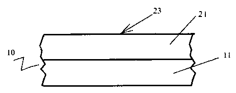
drawings. Referring to figure 1, an electrographic element
(10) is shown for use in the present invention. The element
comprises a conductive base (11) and an imaging layer
structure (21) coated over said base. The imaging layer
structure (21) has an imags receptive surface (23).
The base (11) functions as a support to the superposed
layers and may be any web or sheet material possessing
suitable flexibility, dimensional stability and adherence
properties to those layers. Typically, the base will have an
electrical resistivity of about 1 to 30 meg-ohm per ~.
Suitable web or sheet materials for the base are
flexible polymeric films, e.g., such as polyethylene
terephthalate film and the like, or a foraminous material,
e.g., such as a paper sheet and the Like, treated to be
electrically conductive or semi-conductive. Other suitable
materials are for instance, metal foils, metallized
polymeric films such as polyethylene terephthalate films
having a metallic coating thereon, conductive paper sheeting
and the like.
As shown in figure 2, the base may itself comprise a
multilayer structure. In its simplest form, the base may
include a carrier sheet (12) which is conductive, having a
front side (17) and a back side (13) The front side (17) is
covered by a release layer (15) over which is placed the
imaging layer structure (21)~ In an alternate embodiment, a
conductive layer (14) is coated over the carrier sheet (12)
between the carrier sheet and the release layer. In yet
another embodiment, the back side (13) of carrier sheet (12)
is also covered by a conductive layer (19).
When the base comprises a carrier sheet (12), the
carrier sheet (12) is again a flexible web or sheet
material, which may again be a flexible polymeric film,
e.g., such as polyethylene terephthalate film and the like,
or a foraminous material, e.g., such as a paper sheet and
the like. A conductive layer (14) may be coated over the
carrier sheet (12) or the carrier sheet (12) may or may not
be itself conductive.
5
~'~ 94122667 ~-~,~ ~~' ~~~~'//~11~9~1~3(2~
The conductive layer (14) preferably comprises a filrn-
forming material which may be an organic material, e.go,
such as a ration type styrene-methacrylate copolymer having
an electrical resistivity of about 1 to 30 meg-ohm per ~.
Other suitable film-forming, organic materials include
polymeric quaternary ammonium compounds, polystyrene
sulfonic acid, polymeric matrices capable of ionising
inorganic electrolytes contained therein, and the like. The
film-forming, organic material may be eased alone or with
l0 conductive, inorganic materials and/or metals dispersed
therein, e.g., such as tin oxide, aluminum and the like.
The release layer (15) which is adhered to the front
surface (17) of the base (11) or to the conductive layer
(14) as shown in figure 2, typically comprises a film
forming silicone polymers or a film forming fluoropolymer.
The release layer may also be heat cured, IJa~l. radiation
cured, or electron beam cured. The release layer may itself
be conductive or contain conductive agents such as a
quaternary ammonium polymer, and may further include a
surfactant. Good release performance has been obtained when
the surface energy of the release layer is between 20 and 40
dynes/cm and preferably between 25 and 35 dynes/cm.
The imaging layer structure (22) used in this invention
is transparent. A transparent imaging layer structure is
one in which the layers and combination of layers of the
structure, allow sufficient radiation transmission in at
least one region of the visual spectrum to allo~r the visual
observation of a toned image placed on one side of said
layer structure from the other side of the layer structure.
The imaging layer structure (21) may also comprise one
or more distinct layers each having a specific functiono
Figure 3 shows such a structure which includes a protective
layer (19), a dielectric layer (20), an adhesive layer (22)
and may avers include a conductive layer (18)D placed in the
order shown. All of these layers must be transparent. In
the simplest form the imaging layer structure includes only
the dielectric layer (20).
6
'V~ 94!22667 TIL7S941p3626
The dielectric layer (20), may be any conventional
film-forming material having a dielectric constant of about
2 to about 5. This layer typically has a thickness in the
range of about 1 ~m to about 20 ~m and preferably in the
range of about 5 ~,m to about 15 ~,m. The layer (20),
typically comprises one or more polymers selected from
polyvinylacetate, polyvinylchloride, polyvinylbutyral,
polymethylmethacrylate, styrenated acrylics, styrene
acrylonitrile, and the like. ~ther ingredients may be
chosen from waxes, polyethylene, alkyd resins,
nitrocellulose, ethylcellulose, cellulose acetate, shellac,
epoxy resins, styrene-butadiene copolymers, clorinated
rubbers, polyacrylates, and the like. The property
requirements of the dielectric layer (20) are well known in
the art as disclosed, for example, in U.S. Patents 3,920,880
and 4,201,701.
It is preferred for this layer to have a high degree of
transparency< Transparency is aided by avoiding the use of
opaque pigments, and by minimizing the content of other
pigments, light scattering or light absorbing materials.
Preferably the dielectric layer is formulated for
solvent coating, or it may be formulated from hot melt
extrudable resins and coated using hot melt extrusion
techniques.
Still referring to figure 3, the imaging layer
structure may include in addition to the dielectric layer
20, an adhesive layer (22) as a separate layer.
The adhesive layer (22) may be a substantially tack-
free, thermal adhesive which is activated at a pressure and
a temperature that is above the normal ambient pressure and
temperature of the electrographic element prior to use. The
adhesive layer (22) may be chosen from a variety of
conventional thermal adhesive materials. Typically, the
thermall,~ activated adhesive material is comprised of
thermoplastic polyurethanes; polycaprolactone; acrylic
copolymers; and combinations thereof. Representative
thermally activated adhesive materials include Morthane~
7
~ ~ 5°~9~~
1f ~ 94122667 I~c~°f 1~J~94I~3626
CA-116 urethane resin (a product of P~orton International)a
Tone~ Polymer P767E biodegradable plastic resin (a product
of Union Carbide); Elvax~ 240 vinyl resin (a product of
Dupont Chemicals); and the liken The adhesive layer (22) is
visually transparent in at least one region ~rithin the
visible spectral region and typically is transparent
throughout the visible spectral regiono
The surface of the adhesive layer (22) may be rough to
ensure good transfer of charge during passage of the element
under the stylus bar during imagingo This roughness can be
obtained by including in the layer particles sufficiently
large to give surface irregularities to the layers
Particles of diameter in the range of about 1 dam to about 15
~m are suitableo Particle composition and size are chosen
to give the required dielectric constant to the layer as
well as the appropriate surface topography and abrasive
properties to the layer
It is contemplated that in performing the process of
this invention° the adhesive layer may be placed not on the
electrographic elemente brat on the surface of a substrate
serving as a permanent receptors on which it is desired to
transfer the electrographic image as described bellow as
shown in figure 11o In that case° prior to the transfer
stepo the surface of the permanent receptor that ~ail1
receive the image° is coated with an adhesive to form an
adhesive layer (22°)o In that case° the adhesive may be one
that is spayed thereon ° a o g a 3M Scotch'' Brand Spray P~ount~'~
Artists Adhesive° particularly where the surface or overall
nature of the receptor is such that other coating methods
are impractical; or the adhesive may be coated with a
rollers or again applied by lamination or other coating
techniquesm
The adhesive layer (22°)° may exhibit tackiness at room
temperatures° or may be non tacky at room temperatures and
be heat or pressure activatede Heat activated adhesive
layers may be chosen from a variety of conventional thermal
adhesive materials and may be the same as described above
8
V~ 94122667 ~'y'CT/L1S94I03626
for use in the adhesive layer (22). On the other hand,
adhesives used on the receptor surface need not be
transparent.
The adhesive layer (22') on the receptor surface, may
be created jujt prior to image transfer, or may be created
ahead of time at a different location from where the
transfer is to occur. If tacky at room temperatures, the
adhesive layer (22°), may be protected with a removable
cover sheet which is be removed prior to use and discarded.
The electrographic element may be formulated to provide
the necessary resistance to abrasion and U.V. or other
detrimewtal radiation as well as contain biocides and
fungicides to act as a protective layer. The use of ~utvar~
polyvinyl butyral in the dielectric formulation for instance
results in a dielectric layer with excellent resistance to
scratching. In an alternate embodiment, a protective layer
(19) separate from the dielectric layer may be provided, as
shown in figure 3.
The protective layer (19) is a polymeric film material
which is resistant to scratching, abrasions and the like,
and to environmental components and contaminants, and may
also include biocides and fungicides. The protective layer
(19) is also visually transparent in at least one region
within the visible spectral region and typically is
transparent throughout the visible spectral region.
Polymeric: materials which are useful in making this layer
include polyvinyl chloride; polyvinyl butyral~ cellulose
acetate propionate~ cellulose acetate butyrate; polyesters;
acrylics; polyurethanes; styrene copolymers, e.g., such as
styrene acrylonitrile~ and combinations thereof. This
layer typically has a thickness in the range of about 0.5 dam
to about 10 hum and preferably in the range of about 1 ~.m to
about 4 ~,sm. Such layer typically will withstand scribing
with the point of a 4H pencil without breakthrough.
In certain instances it may be desirable to include a
transparent conductive layer (18) as a part of the imaging
layer structure. Such layer may be formulated to act as a
9
~ ~ 5~~ ~°,,
~'~ 94122667 lID~~°II~J~9~1~3626
release layer between the base and the image structure
layer, by adapting it to adhere more strongly t~ the
dielectric or the pr~tective layer as the case may be, than
to the base~
The conductive layer (18) comprises a film-forminc~a
organic material, a~go, such as a cation type styrene-
methacrylate copolymer having an electrical resistivity of
about 1 to 30 meg-ohm per ~~ Suitable film-forming, organic
materials include polymeric quaternary ammonium compounds,
polystyrene sulfonic acid, polymeric matrices capable of
ionizing inorganic electrolytes contained therein, and the
liken The film-forming, organic material may be used alone
or with conductive, inorganic materials and/or metals
dispersed therein, sago, such as tin oxide, aluminum and the
liken
Figure 4 shows a preferred electrographic imaging
element in acc~rdance with the present invention which
comprises a base comprising a conductive carrier sheet (12)
and a release layer (15)m The element further includes a
combined dielectric and adhesive layer (16)o This combined
dielectric and adhesive layer (16), may be any conventional
transparent film-forming material having a dielectric
constant of about 2 to ab~ut 5o This layer typically has a
thickness in the range of about 1 ~Sm to about 20 ~Sm and
preferably in the range of about 5 ~m to about 15 Imo
This transparent combined dielectric and adhesive layer
(16) typically comprises one ~r more polyestersa
polyurethanesa polyamidesA polyolefinse polycarbonatesa
polystyrenes~ and/or polymers or copolymers of acrylic or
methacrylic acids, esters, amides, or the like (such as
polymethylmethacrylate), styrenes, acrylonitriles, vinyl
esters, alkyd substituted vinyl esters, vinyl alcohol, vinyl
acetals (eeg~, polyvinyl butyral), vinyl chloride, vinyl
o fluoride, vinylidene chloride, 1,4-dienes (eegea butadiene,
isoprene and the like)B ethylene/vinyl alcohol copolymerso
copolymers of styrene with acrylic and methacrylic monomersp
modified cellulosic resins such as cellulose acetate and
21 ~~~9~.
'~U~ 94122667 lPCT/US94/03626
cellulose acetate butyrate; block copolymer thermoplastic
rubbers (e. g., styrene/ethylene/ butylene/styrene block
copolymer); and blends of the above.
The combined dielectric and adhesive layer (1~) in
addition to its dielectric properties, is activated at a
pressure and, optionally, at a temperature that is above the
normal ambient pressure and temperature of the
electrographic element prior to use to exhibit its adhesive
properties. Thus the combined dielectric and adhesive layer
is non tacky prior to activation.
The surface of the imaging layer structure (21) may be
made rough to ensure good transfer of charge during passage
of the element under the stylus bar during imaging. This
roughness can be obtained by including in the uppermost
layer particles sufficiently large to give surface
irregularities to the layer. Particle composition and size
are chosen to give the required surface topography and
abrasive properties to the layer. Particles of diameter in
the range of about 1 ~m to about 15 ~Cm are suitable.
The imaging layer structure (21) may contain in any of
its layers, components which strongly absorb ultraviolet
radiation thereby reducing damage to underlying images by
ambient ultraviolet light, e.g., such as 2-hydroxy-
benzophenones~ oxalanilides~ aryl esters and the like;
hindered amine light stabilizers, such as bis(2,2,6,6-
tetramethyl-4-piperidinyl) sebacate and the like; and
combinations thereof. The .imaging layer structure serves as
a protective layer to the transferred toned image after the
image has been transferred onto a receptor substrate as will
be described bellow, and is preferably selected to withstand
scribing with the point of a 4H pencil without breakthrough.
At times it is desired to provide a range of surface
finishes to the finished image. This is done by controlling
the surface of the image layer structure in contact with the
release layer on the base. The nature of this surface will
depend on the nature of the surface of the release layer in
contact therewith. Thus if the release layer on the base
11
~'~ 94122667 ~ ~ ~ ~ ~ ~ ~ ~~1°/~J~94I~3626
has a rough textures the final image will appear matteD and
if the release layer surface texture is smooth~ the final
image will be glossya
Alternatively a matte surface on the finished image
can he obtained by including in at least one of the layers
of the image layer structure particles sufficiently large to
give surface irregularities to the layers Particles of
average diameter in the range of about 1 ~Cm to about 15 ~Sm
are suitablem
The novel electrographic imaging process comprises the
following stepso
An electrographic toned image is created on the image
receptive surface (23) of the imaging layer structure (21)
of an electrographic element of the type described shoves
This is typically done using an electrographic printer of
the type shown schematically in figure 5o Such printers are
well known in the art and typically may comprise an image
source which may be a computer (40)g and a mechanical
arrangement for generating an image on an electrographic
elements The computer (40) in addition to providing image
information to the printing station of the printers usually
also controls all functions of the printero including
driving an electrographic element (10) through an imaging
station (43) which may comprise an array of styli (44)o The
computer addresses the styli and instructs them to deposit a
predetermined amount of charge on the image receptive
surface (23) of the electrographic elemento A latent image
in the form of a charge distribution is thus formed on the
image receptive surface (23) of the electrographic element
(10)~
The element is next transported through a toning
station (46) where an appropriate toner is applied onto the
image receptive surface to produce a toned image (4~) as
shown in figure 6m The toning station may include a fixing
substation where the applied toner is fixedg by dryings heat
or pressure or any combination thereofo onto the image
receptive surface (23)e
12
~59~94
'V~ 94/22667 PCTII7S94/03626
When a colored image is desired to be reproduced the
above process is repeated with additional toners of
different colors, in either sequentially arranged imaging
and toning stations or by passing the element under the same
imaging station and replacing the toner in the toning
station. Color reproduction usually requires three and
preferably four different color toners to render a pleasing
and accurate facsimile of an original color image. The
selection of toner colors and the creation of the different
images whose combination will provide such accurate
rendition of an original image is well known in the art and
not the subject of the present invention.
The image (48) created on the image receptive surface
in accordance with the present process is a mirror image of
the desired reproduction.
The image (48) is next transferred onto a permanent
receptor (50), which may be any substrate on which one
desires ~to have the image placed. Figure °7 illustrates this
step. Figure 9 is an elevation cross section taken along
'9-9' of figure 7, showing the imaged element adhered onto
the permanent receptor (50) following lamination. The
permanent receptor (50), typically functions as the final
support for the imaged electrographic element formed during
the process steps of this invention.
The permanent receptor (50) may be any substrate having
a surface upon which an electrographic image is to be placed
for display. Typically, it is a web or sheet material
possessing dimensional stability and adherence properties to
the toned image layer of the imaged electrographic element.
3D The web or sheet material may be a flexible polymeric film,
e.g~, such as polyethylene terephthalate film and the likes
a foraminous material, e.g., such as a paper sheet, textile
fabrics, and the like; metal films or webs, e.g., such as
aluminum, steel, tin-plate, and the like; or any composites
or laminates thereof. The permanent receptor may be a
rigid or semi-rigid sheeting or plate; e.g., such as
sheeting or plates of metal, glass, ceramic, plastic,
13
W~ 94122669 ~~~'//~159~/03626
cardboard, prick wallD papers~ paperboardsg wood~ leathers
and composites of the above or laminates thereof. The
permanent receptor may vary in size from that of a
photographic print~ e.g.o having an area of about 30 cmz or
less~ to that of billboardso e.g.~ having an area of about
70 m2 or greater. The permanent receptor may also be
surface treated or coated with a material to enhance desired
surface characteristics.
Then the adhesive layer is not part of the image 1_ayer
structures prior to the transfer steps the surface of the
permanent receptor that will receive the imageo is coated
with an adhesive to form adhesive layer (22g)o The adhesive
may be spayed thereonp or it may be coated with a rollerA
or again applied by lamination or other coating techniques.
After the image has been produced on the elemento and
the adhesive layer when so required produced on the
receptor, the receptor substrate is preferably pressure
laminated onto the surface of the toned image layer
structure (21) of the imaged electrographic element (10)e
preferably at a temperature which is above the ambient
temperature. Referring to Figure 10~ the receptor substrate
(50) is contacted and pressure laminated to the toned image
layer (21) using an applied pressure (31) to the back side
of the base (11) and receptor substrate (50) to form a
laminated imaged electrographic element (30).
In accordance with the process of the present
invention~ the receptor substrate (50) typically is pressure
laminated to the toned image surface of the imaged
electrographic element (10) under an applied pressure (31)
of about atmospheric pressure or greater but may range from
about 0.5 kg/cmz to about 100 kg/cm~ or more. The term
~°applied pressure°e is intended to mean the absolute pressure
which is applied to a unit area of the surface as
conventionally derived from the geometry of the pressure
means, e.g.d the geometry of the laminating naps in
combination with a measurement means~ e.g.~ a calibrated
gauge pressure. Suitable means that may be used to apply
14
'~'~ 94/22667 PCT'/g7S94/03626
pressure include platen presses; counterpoised, double roll,
laminating devices; scanning, single roll, laminating
devices vacuum laminating devices; and the Like. When the
receptor substrate (50) has an air impervious surface, roll
laminating devices are preferred since they readily minimize
air entrapment between the toned image layer and the
receptor substrate during the pressure laminating process
step. Vacuum may be applied with such devices to further
eliminate air entrapment. When the receptor substrate (50)
is rigid and roll laminating devices are used, the flexible
imaged electrographic element (10) typically is pressure
laminated to the receptor substrate (32).
Heat may be used in the pressure laminating step (step
(B)) of this invention to raise the temperature of the
adhesive (22), (22'), or combined dielectric and adhesive
layer (1~) from its normal ambient temperature (e. g., room
temperature) where it is substantially tack-free, to a
temperature at which the adhesive properties are activated.
Heat may be applied to the adhesive or combined dielectric
and adhesive layer prior to and/or concurrently with the
application of the applied pressure (31). Thus, the
receptor substrate (50) and/or the imaged electrographic
element (10) may be heated prior to pressure lamination by
radiant or contact heaters and then laminated while hot.
Alternatively the pressure means itself may also function as
a heater, e.g., such as a hot roll laminator, or both prior
and concurrent heating may be used in combination.
Typically, a laminating temperature of about 100°C or
greater Ls employed. Typically, temperature is measured on
the surface of the heated roll or platen by means of
temperature sensitive tape.
USlIlg the process of this invention, surprisingly
strong adhesion of the toned electrographic element (10) to
the receptor substrate (50) is achieved with substantially
no image distortion, even though the toned image layer (48)
is interposed between the imaging layer structure and the
receptor substrate (50).
W~ 94122667 ~~~'/~TS94/~362
If the base is also transparent and if the particular
application so requires, the process is terminated at this
pointm However it is usually preferred to use inexpensive
carrier sheet for the base which is neither transparent nor
does it weather satisfactorily, so in the preferred mJde,
the base is stripped from the laminated element, leaving the
image receptive layer overlaying the toned image to act as a
protective layer for the transferred image to protect the
image from scratching, abrasions, environmental components
and contaminants, and the liken
Referring again to Figure 10, the base layer {11) is
peeled off, using a peel force (41), from the surface of the
image layer structure (21) to form an imaged electrographic
elementm Typically, the base layer (11) is peeled with a
peel force (41) directed at an angle of 90~ ~r more from the
surface of the image layer structurem The peel rate and the
peel force (41) are not critical and preferred values will
depend on the nature of the conductive and carrier
materialse The temperature at which the base layer (11) is
peeled from the image layer structure will depend on the
properties of the release layero Surprisingly has been
found that the base layer (11) can be removed immediately
after formation of the imaged electrographic element (30)
(i~em, while still in a heated state from the lamination in
the second process step) without delamination of the imaging
layer structure {21) or any of the component layerso In
this context, the term ~Himmediatelyae is intended to mean a
time span of about 1 minute or less and preferably between
about 1 second and about 20 secondsm Still more preferably
the base is removed after about 5 to 10 secondso
In the practice of the process of this invention where
the base layer is to be removed, it is preferred to keep the
base layer in place on the imaged electrographic element
throughout storage and processing in order to prevent any
damage or marring to the underlying layerso In this
instance, removal of the base layer is the very last step in
preparing and mounting the protected electrographic imageo
16
f~ 94/22667 f//I1S94103626
As has also been surprisingly found, the base need not
be removed immediately. The formed laminated imaged
electrographic element (30) may be cooled and stored before
removal of the base. In this instance, the base layer (11)
can be removed at room temperature from the imaged
electrographic element (30) without delamination of the
image layer structure from the receptor.
Alternatively, the imaged electrographic element (30)
may be reheated prior to removal of the base layer (11).
The electrographic process of this invention will now
be illustrated by the following examples but is not intended
to be limited thereby. A number of products by different
manufacturers are used in this invention and in the examples
below. 'rhe following is a reference table for identifying
such products and their respective trade names.
(1) Chemistat~ 6300H electroconductive polymer is a
product of Sanyo Chemical Industries and is a cation type
styrene-:rnethacrylate copolymer in aqueous solution.
(2) Butvar~ B-76 polyvinyl butyral (weight ave.
moleCUlar weights 90,0~~-120,0~~) is a product of Monsanto
Company, St. ~.OL11S, M3.SSOUrl.
(3) Butvar~ B-79 polyvinyl butyral (weight ave.
molecular weight: 50,000-80,000) is a product of Monsanto
Company, St. Louis, Missouri.
(4) E-342 Acrylic resin is a product of Rohm and Hass
and is a solvent based modified acrylic copolymer.
(5) Syloid~ amorphous silica is produced by Davison
Chemical Division, W.R. Grace & Co., Baltimore NTd. in
various average particle sizes
(6) Hydrocarb~ PG3 wet ground calcium carbonate with
average particle size of 3 dam is a product of ~MYA, Proctor,
Vermont.
(7) Piccolastic~ A°5 low molecular weight polystyrene
is a product of Hercules Co., Wilmington, Delaware.
(8) Dowanol~ PP2 is propylene glycol mono methyl ether
and is a product of Dow Chemical Corp.
(9) Kraton~ FG-1921X is a styrene ethylene butylene
17
VV~ 94122667 ~ ~°/~JS~~I~366
styrene block copolymer thermoplastic rubber and is a
product of Shell Oil Company, Houston, Texase
(10) Calcined clay is Translink~ calcined clay, and is
a product of Englehard Corporation, Edlson, ~oJa
(11) Lustran~ '?3-1000 SAID resin is a styrene-
acrylonitrile copolymer and is a product of T~Ionsanto
Company, Stm LOU1S, I~issour1m
(12) Morthane~ CA-116 urethane resin is a hydroxyl
terminated polyurethane elastomer and is a product of
F2orton-Thiokole
(13) Cellulose acetate propionate is Co~oPo 504-Oa2
cellulose ester, a product of Eastman Chemicalso
(14) Hexamethoxymethylmelamine is Cymel~ 301 melamine-
formaldehyde crosslinking resin, and is a product of
Cyanamid Corporationo
(15) Chemistat~ 7005 electroconductive p~lymer is a
product of Sanyo Chemical Industries and is an aqueous
solution of a polycationic water-soluble ~rganic polymer>
The light yellow liquid contains approximately 40 % active
ingredients, has a pH of 4a5, and a viscosity at 25°C of
330 cpse
(16) Polycaprolactone which is Tone~ Polymer P-767E
biodegradable plastic resin, a product of Union Carbideo
Example 1
An electrographic element having the structure shown in
figure 2, was prepared as followso A 70 g/m2 opaque
conductive paper available from Chartham Paper mills,
Canterbury, Kent, IlmK~ was coated by the reverse gravure
method with a silicone release layer (STI ~~QgCeB available
from Release International, best Chicagog Illinois) at a
coated weight of 1m46 g/ma and cured by electron beam
radiatione This formed a conductive carrier sheet having a
release layer thereone The surface electrical resistivity
of the release layer measured at 50% relative humidity (RH)
was 9 Mohm/square, the surface energy was between 25 and 30
dynes/cm, and the Sheffield Smoothness was 25 ml/mine
A conductive coating was prepared from the following
18
fO 94122667 ~ ~ P~TlLTS94I036~6
- ingredients:
Ingredient Parts by Weight
Ethanol 57
Water 19
Chemistat~ 6300H'1' 24
The three ingredients were mixed together with a
Lightnin Mixer for 10 minutes.
This coating was applied to the side opposite the
release coating on the conductive paper by the rod coating
method a~t a wet coat weight of 15.& g/m2 and dried. The
resulting coated conductive paper formed the conductive base
for this element.
A combined dielectric and adhesive coating mixture
which also has protective properties, and wherein the
adhesive properties are heat activated, was prepared from
the following ingredients:
Ingredient Parts by Weight
Ethanol 120
Acetone 440
Toluene 720
Butvar W-76'x' polyvinyl butyral 130
E-342'°' Acrylic Resin 440
Syloid~ 74'5' Amorphous silica 20
Hydrocarb~' PG3'6' 175
Piccolastic~ A-5 "'
52
The first three of the above ingredients were added to
a Kady mill and the Butvar~' was stirred in. After 15
minutes of mixing the acrylic resin and the polystyrene were
added. After a further 5 minutes of mixing the calcium
carbonate and the amorphous silica were added and the mixing
continued for 10 minutes.
The above dielectric mixture was applied to the release
coated surface of the conductive base paper by reverse doll
coating and dried to give a dry coat weight of 7.3 g/ma, to
form the electrographic element.
19
~'~ 94/22667 ~. ~ ~ ~ ~ ~~~t'lttJS94l~3626
Rolls of the electrographic element were moisturized to
a level of from 6 to 7o by weight and a four color toned
image layer was deposited on the adhesive protective
dleleCtrlC layer using a Versatec~ 8944 Color Electrostatic
Printer (a product of Xerox Enginee~inr~ Systemsa San Jose~
California) using standard toners and plotting conditionsa
Observed image quality was rated highs
The element was next laminated onto a receptor surface
by first laying the imaged electrographic element on a
receptor sheet of ScotchCalT~' 220 pressure sensitive vinyl
(a product of 3M Cooa Ste Paul~ Minnesota) with the toned
image in contact with the receptor sheets This composite
was then passed through the hot nip of an IT 6000 hot roll
laminator (obtained from Image Technologies Corpoe Cottage
Grove, WIo) at a speed of Oo6lm/min~ at a temperature of
121~C and a pressure of 7003 Kg/cm2~ The base sheet was
removed approximately 10 seem after the laminated composite
was removed from the hot nipo The toned image and the
dielectric coating remained adhered to the vinyl and the
release coating remained on the papero
The image surface had a low glare surface with a °75°
gloss of between 30 and 35%m The image was not removed by
810 ScotchT" Brand Tape when tested with the tape pull
procedures The image withstood cleansing with common non-
abrasive household cleaners and scrubbing with a nylon
bristle brushm
Examt~le 2 m
An imaged electrographic element prepared as disclosed
in example 1 above was laminated onto a Hi-Stat~ Static
Cling Vinyl receptor substrate using the laminator and
laminating conditions also disclosed in example 1a ~i-Stat~
Static Cling Vinyl is a product of Catalinao of Calabassasa
Californian Results were similar to the.results of
example 10
Example 3 a
An imaged electrographic element prepared as disclosed
in example 1 above was laminated onto a Saturn ~paque
VO 94/22667 PC~'/I1S94~03626
Banners Vinyl receptor substrate using the laminator and
laminating conditions also disclosed in example 1. Saturn
Opaque Banner Vinyl is a product of ICG Co., Kingsport,
Tennessee. Results were similar to the results of
example 1.
Example 4.
An imaged electrographic element prepared as disclosed
in example 1 above was laminated onto an Ultramag~ Vinyl
Coated Magnetic Material receptor substrate using the
laminator and laminating conditions also disclosed in
example 1. Ultramag° Vinyl Coated Magnetic Material is a
product of Flexmag Industries, Cincinnati, ~hio. Results
were similar to the results of example 1.
Example 5
An imaged electrographic element prepared as disclosed
in example 1 above was laminated onto a Komatex~ Rigid PVC
Board used as the receptor substrate, using the laminator
and laminating conditions also disclosed in example 1.
Komatex~ Rigid PVC Board is a product of Kommerling Co. of
Germany, distributed in this country through Kommerling
Co., Montvale, New Jersey. Results were similar to the
results of example 1.
Example 6
A roll of an toned, imaged electrographic element
prepared as disclosed in example 1 was mounted on the top
feed spool of an IT 6000 hot roll laminator and threaded
through the nip so that the base side of the element
contacted the top hot roll for several inches before the
nip. A :roll of ScotchCal'i''~ 7725 pressure sensitive vinyl (a
product of 3M Co., St. Paul, Minnesota) was mounted on the
bottom feed spool and threaded through the nip so that vinyl
side was in contact with the image side of the
electrographic element. The composite was laminated in the
hot nip at a speed of approximately 0.61m/min, a temperature
of 121'C and a pressure of 7.03 Kg/mz. The laminated
composite was collected on the take-up spool of the
laminator. The base was removed approximately 5 minutes
21
~~ 94122667 ~~ ~ I~~~°I~7~~%~/~3626
laterm The image and the dielectric coating remained adhered
to the vinyl and the release coating remained on the basee
Exam~l a 7
An electrographic element was prepared as followso
A 63 g/m opaque conductive paper available as Product I~R
Sase from Otis Specialty Papersa Livermore Fallsa l~Iaine~ was
coated by the offset gravure method with a silicone release
layer identified as SY~ 9fa~C~~ available from Release
International~ West Chicagoa Illinois at a coated weight of
1x95 g/m~m The release layer was cured after coating by
electron beam radiationm The surface electrical resistivity
of the release coated surface measured at 50% F2H was
3 Mohm/square~ the surface energy was between 25 and 30
dynes/cm~ and the Sheffield Smoothness was ~0 ml/mino
A combined dielectric/adhesive coating mixture having
protective and heat activated adhesive properties prepared
as described in example 1 was applied to the release coated
surface of the conductive base paper by the reverse roll
coating method and dried to give a dry coat weight of
703 g/m2 to form the electrographic elements
Rolls of the electrographic element were moisturized to
a level of about 6% by weight and a four col~r image layer
was deposited on the adhesive protective dielectric layer
using the Versatec~ 8944 Color Electrostatic Printer of
example 1 and standard toners and plotting conditionso
Image quality was rated highe
The toned element was next laminated on a receptor
sheet of ScotchCalT~° 220 pressure sensitive vinyl in the
same manner as described in example io Following laminations
the base was removed approximately 10 sacs after the
composite was removed from the hot nipe The image and the
combined dielectric and adhesive coating remained adhered to
the vinyl while the release coating remained on the
conductive paper~
The image on the receptor sheet~ had a lour glare
surface with a 75° gloss of between 40 and 45%m It
withstood gentle scribing with 4H and 8H pencilsm
22
V~ 94122667 PCT°ILJS94l~3626
Example 8
An alternate combined dielectric and adhesive coating
was prepared from the following ingredients:
Ingredient Parts by Weight
Toluene 42.50
Kraton~ FG-1921X ~~' 7.50
Dowanol~ PM ~$' 2.93
Toluene 24.59
Methyl ethyl ketone 9.55
Calcined clay ~l°' ( ave. particle size 1. 4 dam) 0. 50
Syloid~ 74 Amorphous silica c5' 1.05
Lustran~ 33-1000 SAN cll' resin 11.38
The toluene was added to a vessel and stirred with a
Lightnin mixer. The Kraton~' was added slowly and mixed
under slow agitation. The remaining ingredients were added
in the sequence shown and mixed with a Dispermat~ mixer
under slow speed agitation and then allowed to mix for 10
minutes at high speed. The two mixtures were then blended
in a vessel and stirred at slow speed with the Dispermat~
mixer.
The mixture was coated onto a base such as described in
example 1 with a No. 12 Meyer rod and dried in an air oven
at 116°C for 30 sec. to form an electrographic element
having transparent combined dielectric and adhesive layers.
After conditioning a sample of the electrographic
element at 50 % relative humidity a toned image was produced
on the sample by using a versatec V-80 electrostatic plotter
operated at conventional plotting conditions.
The laminating step was next performed as described in
example 1 except that the receptor substrate was Rexcal°
4000, a pressure sensitive vinyl polymer available from
Rexham Branded Products, Lancaster, South Carolina.
Following lamination, the base was stripped from the
combined dielectric and adhesive layer comprising the image
layer structure, with the break occurring between the
release layer on the base and the combined dielectric and
adhesive layer on the image layer structure.
23
W~ 94122.667 ~c~°fI~JS94/~36~r~
Example 9
An electrographic element was prepared a s followsm A
conductive coating solution was prepared from the following
ingredientso
Ingredient Parts 8~l ~41e1~
Methyl alcohol 80x0
Deionized water 12m0
Chemistat~ F300H'1' 8 m 0
The above ingredients were added in the order shown and
1o mixed in a Lightnin~ mixer for 5 minuteso Th e coating was
then applied to a ~50 ~sm (2 mil) thick~ untre ateda
polyethylene terephthalate film with a meyer rod and dried
in an air dried oven at 115~C for two minutes to give a dry
coating thickness of 2m0 ~mm
A dielectric layer coating solution was prepared from
the folloGaing ingredients o
Ingredient Parts Hy Weight
Propylene glycol monomethyl ether 7e32
Toluene 21096
2~ E-342 AcryllC reslTl'~' S6 0 44
Syloid~ 74'5' Amorphous silica 12058
Translink'3' 77 Calcined clay~
(aveo particle size 0~8 ~m) 1e70
The above ingredients were added as shown and mixed
using a Cowles dispersion mixer for 10 minutesm The
solution was overcoated onto the previously coated film
using a meyer rod and dried at 115~C for tyro minutes to give
a dry coating thickness of 5m0 ~Cma
An adhesive layer coating solution was prepared from
the following ingredientso
Incrredient Parts 8v Weight
Methyl ethyl ketone °7°7096
Toluene 10000
Morthane~ CA-116'12'urethane resin 12°00
Syloid~'5' Amorphous silica (ave~ particle size 3 Vim) Oo04
The coating solution was made by mixing the methyl
24
15594
~~ 94122667 PCT'/LTS94/03626
ethyl ketone, toluene and urethane resin for 30 minutes with
a high speed Lightnin~ mixer. Amorphous silica was then
added and mixed for 5 minutes. The solution was overcoated
onto the previously coated film using a meyer rod and dried
ai: 115°C for two minutes to give a dry coating thickness of
2.0 ~cm to form the electrographic element.
The imaged layer was applied to the surface of the
imaging layer structure of the electrographic element formed
above, by using a Versatec~' V-80 electrostatic plotter
operated at conventional plotting conditions.
The laminating step was performed by first laying the
imaged electrographic element on a sheet of 201bs
xerographic bond paper so that the imaged layer contacted
the paper sheet. This composite was then passed through the
hot nip of a hot roll laminator at a speed of 2.54 cm per
second a:nd at a pressure of 30 Kg/cm2. The hot nip
consisted of a heated steel roll at a temperature of 115°C
and a hard polyurethane backing roll of a B.F. Perkins
laboratory calendar. The laminated composite exiting the
hot nip ~uas allowed to cool to room temperature and the
polyethylene terephthalate film was left in place, adhered
to the conductive coating, where it functioned as a
protective cover sheet for the finished electrographic
element.
Example 10
The process of Example 9 was repeated except that the
laminating step was performed by first laying the imaged
electrographic element on a a_00 ~sm (4 mil) thick white vinyl
film sheet so that the imaged layer contacted the vinyl
sheet. This composite sample was then laminated as in
example ~ using E.F. Perkins laboratory calendar. Within 10
seconds of the exit of the laminated composite from the hot
nip, the polyethylene terephthalate support contiguous to
the conductive layer was stripped therefrom.
Example 11
An electrographic element containing an interposed
protective layer was made as followse An abrasion resistant
~'~ 94!22667 ~~, ~ ~~?T'/~JS94I~3~2~
coating solution was prepared from the following
ingredientsm
Incrredient Parts By Weight
Dowanol PM'8' 30 0 41
Ethyl acetate 26041
Toluene 10096
Butyrolactone 9026
CmA~Pe 504-Om2'13' Cellulose acetate propionate 20006
Cymel~ 301'1' Hexamethoxymethylmelamine 2064
Para-toluene sulfonic acid Oa53
Syloid~'5' Amorphous silica (avee particle size 3 ,gym) 0001
The cellulose acetate propionate was added to the solvent
blend slowly under a high speed Lightnin~ mixero l~hen fully
dissolved~ the amorphous silica was then added and mixed for
five minutese The melamine resin and acid catalyst were
added and mixed for an additional 15 minutesm The resulting
lacquer was then coated on a ~25 ~Sm (1 mil) thicka
untreated, polyethylene terephthalate film using a meyer rod
and dried at 115~C for two minutes to give a dry coating
thickness of 205 ,umo
A conductive coating solution was prepa~°ed from the
following ingredientsm
Ingredient Parts B~ Weight
3~ethyl alcohol $Oo0
Deionized water 1200
Chemistat~ 6300H'1' $ a 0
The above ingredients were added in the order shown and
mixed in a Lightning mixer for 5 minuteso The coating was
then applied to the surface of the protective coating with a
meyer rod and dried in an air dried oven at 115~C for two
minutes to give a dry coating thickness of 200 ~ma
A dielectric layer coating solution was prepared from
the following ingredientso
Ingredient Parts By ~lei_~
Dowanol~ PNI'$' 7 a 32
Toluene 21096
26
f~ 94/22667 PCT°I~JS94/03626
E-342 Acrylic resin'°' 56.44
Syloid° 74'5' Amorphous silica 12.58
Translinl~°~1°' Calcined clay
(ave. particle size 0.8 ,um) 1.70
The above ingredients were added as shown and mixed
using a Cowles dispersion mixer for 10 minutes. The
solution was overcoated onto the previously coated film
using a meyer rod and dried at 115~C for two minutes to give
a dry coating thickness of 5.0 ~Sm.
An adhesive layer coating solution was prepared as in
example 9 and was coated over the dielectric layer.
A toned image was generated on the adhesive surface of
the imaging layer structure of the electrographic element
formed above, by using a versatec~ V-80 electrostatic
plotter operated at conventional plotting conditions.
The imaged element was laminated on a sheet of 201bs.
xerographic bond paper as in example 9. After the laminated
composite had cooled to room temperature, the remaining
polyethylene terephthalate support was stripped from the
protective layer of the paper backed electrographic image.
The protected electrographic image produced could withstand
scribing with a 4H pencil with no removal of the protective
layer or image.
Example 12
An electrographic element was prepared as followsa A
conductive coating solution which was Chemistat~ 700515' was
applied to a sheet of 551b conductive opaque base paper
(supplied as OCB90 by Chartham Paper Mill, Canterbury, Kent,
U.K.) with a #6 meyer rod and dried in an air dried oven at
115'C for two minutes to give a dry coating thickness of
-2 ~,m .
A dielectric layer coating solution was prepared from
the following ingredients.
Incrredient Parts By Ldeiaht
Toluene
Dowanol~ P~i'~' 22
27
W~ ~~d1226~7 ~~~°II~JS9~I0362~
Polyvinyl butyral (Butvar~ B-"79 '3' ) 10
Syloid°'5' Amorphous silica (eves partials size 3 ~,m) 2
The above ingredients were added in the order shown and
mixed using a Dispermat~ mixer for 15 minuteso The solution
wa:~ overcoated onto the previously coated film using a x'14
meyer rod and dried at 115°C for two minutes to give a dry
coating thickness of °- 3 ~Smo
An adhesive layer coating solution was prepared from
the following ingredients>
Ingredient Parts By Weight
Toluene 85
Dowanol~ PNt'8' S
Polycapr~lactone'a~' 10
The coating solution was made by mixing the ingredients
with a high speed Lightning mixer until the polycaprolactone
was completely in solutionm The solution was overcoated
onto the previously coated film using a ~ meyer rod aa~d
dried at 115°C for two minutes to give a dry coating
thickness of --2 ~,m to form the electrographic elements
After conditioning a sample of the electrographic
element formed above was imaged using the plotter of
example °o
The laminating step was performed by first laying the
imaged electrographic element on an adhesively backed sheet
of ~Oel mm (4 mil) thick untreated cast vinyl polymer having
a removable release liner so that the imaged layer contacted
the vinyl sheets This composite was then passed through the
hot nip of an IT E000 hot roll laminator at a speed of
-1m02 cm/secondg at a temperature of ~- 121°C and at a
pressure of ~ 70 kg/cm2o The laminated composite exiting
the hot nip was cooled to room temperature (5 minutes) and
the two sheets were pulled apart leaving image and
dielectric coatings on the vinyl sheet and the conductive
layer on the conductive paper sheeto
Example 13
An electrographic element was prepared and processed as
described in Example 12 except that the laminating step was
performed by first laying the imaged electrographic element
28
V~ 94/22667 e,
~C°1'ILJS94103626
on a sheet of -- 0.14 mm thick cling vinyl coated with an ink
receptive layer and backed with a 10 pt. paper liner
(Flexmark~ CV600 W, manufactured by Flexcon Co.,
Inc.,Spencer MA.) so that the imaged layer contacted the
vinyl sheet. This composite was then passed through the hot
nip of an IT 6000 hot roll laminator under the same
conditions as in example 12. The laminated composite
exiting the hot nip was cooled to room temperature (1
minute) and the two sheets were pulled apart leaving image,
dielectric, and conductive coatings on the cling vinyl
sheet.
Example 14
An electrographic element was prepared as described in
Example 12 except that the dielectric layer coating solution
was prepared from the following ingredients.
Incrredier.~t Parts By Weight
Toluene 46.1
Methyl ethyl ketone 19.1
Dowanol~ PM'$' 3.8
Polyvinyl butyral (Butvar~ B~76'a') 10.0
Styrene-acrylonitrile copolymer (Lustran~ 33-1000'11') 10.0
Syloid~'5' Amorphous silica (ave. particle size 3 Vim) 3.0
The resulting electrographic element was imaged and
processed as described in Examples 12 and 13, except that as
the resulting laminated composites exited the hot nip, the
two component sheets were pulled apart for each composite,
leaving image and dielectric coatings on the vinyl sheet and
the conductive layer on the conductive paper sheet.
Examx~le 15
An electrographic element was prepared as followsm A
conductive coating solution was prepared from the following
ingredients:
Ingredient Parts By Weictht
Ethyl alcohol 38.0
Deionized water 38.0
Chemistat~ 6300H'1' 24.0
The above ingredients were added in the order shown and
29
bV~ 94/22667 1~~°1~T~941~3626
mixed in a Lightning mixer for 10 minutese The coating
solution was then applied to a -50 ~m (2 mil) thicke
untreatedg polyethylene terephthalate film web using a
reverse roll coater and hot air dried to give a dry coating
weight Of
2 0 ~ g/m2 m
A dielectric layer coating solution was prepared from
the following ingredientse
Ingredient Parts Sy ~eiqht
Dowanol~ PI~~$' 5 m 86
Toluene 49019
Methyl ethyl ketone 19010
Translink° Calcined clay~g°'
(aveo particle size 1m4 dam) 1e00
Syloid~'5' 74 Amorphous silica (Aveo Parto Size 9~m) 2~10
Styrene-acrylonitrile copolymer (Lustran~ 33-100011') 22m75
The above ingredients caere added as shown and mixed in
a Kady Zolver tank under slow speed agitation and then
allowed t~ mix for 60 minutes at high speedo The s~lution
was overcoated ~nto the previously coated film web using a
reverse roll coater and hot air dried to give a dry coating
weight ~f - ~ 0 8 gsm2a
An adhesive layer coating solution was prepared from
the following ingredientse
Ingredient Parts S~ hit
Methyl ethyl ketone 16000
Toluene 64~40
Dowanol ~ ~$' 4 0 0 0
Polycaprolact~ne4l~' 10 a 00
Morthane~ CA-116'12' urethane resin 3 0 00
Calcined clay Translink~~a°a
(aveo particle size 1m4 ~Sm) Om20
Syloid°~5' Amorphous silica (ave> particle size 9 dam) Oo40
The coating solution was made by first adding the
methyl ethyl ketone~ toluene and propylene glycol methyl
ether acetate to a 55 gall~n tub containing a Lightning
mixero The calcined clay and the amorphous silica slurry
b
W~ 94122667 CT/IJS94/03626
were then added and mixed for 30 minutes. Polycaprolactone
was then slowly added under agitation and allowed to mix
until dissolved. The urethane resin was then slowly added
under agitation and allowed -to mix until dissolved. The
resulting coating solution was overcoated onto the
previously coated film web using a reverse roll coater and
hot air dried to give a dry coating thickness of 2.0 ~,m, to
form the electrographic element. Samples of the coated film
web were slit to 36 inch (~ 91.4 cm) width, conditioned at
50% RH a:nd imaged in a Calcomp~ 6800 series color
electrostatic plotter using standard toners and plotting
conditions to form a four color imaged layer on the adhesive
surface of the electrographic element.
The laminating step was performed by first laying the
imaged electrographic element on a sheet of Rexcal~ 4000-000
clear cast vinyl sheet (a product of Rexham Branded
Products, Lancaster, South Carolina) so that the imaged
layer contacted the vinyl sheet. This composite was then
passed through the hot nip of an TT 6000 hot roll laminator
at a speed of 1.02 cm/second, at a temperature of 121°C and
at a pressure of 70 kg/cm2. Within 15 seconds of the exit
of the laminated composite from the hot nip, the
polyethylene terephthalate support contiguous to the
conductive layer was stripped therefrom.
Example 16
An electrographic element was prepared and processed as
described in Example 15 except that the laminating step was
performed by first laying the imaged electrographic element
on a sheet of Rexcal~ 4000-000 clear cast vinyl sheet so
that the imaged layer contacted the vinyl sheet. This
composite was then laminated in a Heat Lamp Vacuum
Applicator (a product of Graco Manufacturing Inc., Niles,
Michigan), using a bake temperature of 118°C and a bake time
of 10 mir.~utes. Within 15 seconds of the removal of the
laminated composite from the Heat Lamp Vacuum Applicator,
the polyethylene terephthalate support contiguous to the
conductive layer was stripped therefrom.
31
~'~ 94/22667 ~ 3~~°~'IUS941~3626
Example 17.
An electrographic element was constructed by extrusion
coating a polymeric resin onto a conductive carrier sheet.
The conductive carrier sheet was conductivized opaque 90
g/m2 paper base ( supplied as OCB90 by Cha~rtha.m Paper ~Lill o
~anterbury~ Kent U.K.).
A. layer of Ethylene Vinyl Alcohol (EVOH) { Kuraray EPE
105A) was extruded onto the base using an extrusion costar
to a coating weight of 9 g/m2 at a coating line speed of 30
m/min. to form an image receptive dielectric layer having
weak adhesion to the carrier sheet.
The coated carrier sheet was then slit to form 11 inch
wide stock web (about 28 cm)a A monochrome toned
electrographic image was produced on the dielectric image
receptive layer with a Versatec V80 plotter. This image was
a mirror image of the desired image.
An adhesive layer coating solution was prepared as in
example 9 and was coated onto the vinyl side of ScotchCalT'~
220 adhesive backed vinyl. The mixture was dried in a
forced air oven for 30 sec at 115°C. The material was
cooled before any use. After cooling the surface was
substantially tack free.
The contacting and adhering step was performed by first
laying the imaged electrographic element from example l on
to the vinyl so that the imaged layer contacted the layer of
urethane. This composite was then passed through the hot
nip of a hot roll laminator at a speed of 0.61 m/min at a
pressure of 6.33 kg/cm2 (cylinder pressure) and at 107°C.
After the composite had cooled to room temperature the base
eaas stripped from the image layer structure. The image on
the vinyl support was viewed through the dielectric layer
and was properly oriented. The image integrity and the
visual quality were retained. The image had an attractive
lustrous appearance.
Example 18.
Using the electrographic element disclosed in example
17 imaged as disclosed in that exampleo the image was
transferred onto a steel surface which had been sprayed with
32
f~ 94122667 PCT'/LTS94/03626
3M ScotchT'~ Brand Spray MountT" Artists Adhesive. The
adhesive was permitted to dry for 1 minute. The contacting
and adhesion step was performed by first laying the imaged
electrographic element so that the imaged layer contacted
the layer of adhesive sprayed onto the steel surface, and
then pressing firmly across the structure. The paper
support was stripped from the image receptive layer leaving
the image on the steel. The dielectric layer acted as a
protective layer overlaying the toner image.
Example 19.
The process of example 18 was repeated but the image
was transferred onto a wood surface that had been coated by
spraying with 3M ScotchT" Brand Spray Mount'~~° Artists
Adhesive.
Example 20.
An electrographic element prepared in accordance with
example 17 was imaged in a Versatec Spectrum color printer
using Cyan, Magenta, Yellow and Black liquid toners. The
image was then contacted and adhered onto a cardboard sheet
having an adhesive coated thereon. The cardboard with the
adhesive coated thereon is supplied by Pres-On I~erchandizing
Corporation of Madison Ill. under the trade name "50 pt.
Claycote, Lo-tack", and exhibits adhesive properties at room
temperature. Following the adhering step, the carrier sheet
was removed and the dielectric image receptive Layer with
the image remained on the cardboard, with the dielectric
layer overlaying the image.
Example 21.
A conductive carrier was prepared by coating w0.50 ~sm
(2 mil) thick untreated Polyethylene Terephthalate film
(PET) with a conductive coating prepared by adding in a
portable mix tank, 38.00 parts of Ethyl Alcohol and 38.00
parts of Deionized Water and mixing therewith with a
Lightning mixer for 10 minutes, 24 parts of Chemistat~ 6300H
containing 80 solids. The coating was applied using reverse
roll coating and hot air drying at 115'C for two minutes to
give a dry coating weight of 2.4 g/m2.
The conductivized carrier sheet was next reverse roll
33
fV~ 94122667 -~~T/~7~9~I036~~
coated with a dielectric layer to achieve a dry dielectric
layer coating weight of 4.8 g/m2. Hot air drying was again
used. The dielectric layer was prepared as followsm
5.86 parts by weight of Dowanol~ PMe 49.19 parts by weight
of Toluene and 19.10 parts by weight of P2ethyl Ethyl Ketone
were added to a Kady Zolver Tank. To the mixture were
added 2.10 parts by weight of Syloid 74 Amorphous Silica and
1.00 part by weight of Translink~ calcined clay under very
slow speed agitation~ and then allowed to mix for 30 minutes
under high speed agitation. After thisa 22.75 parts by
weight of Lustran~(11' 33-1000 were added very slowly under
slow speed agitation and mixed at high speed for 60 minutes.
Samples of this coated material were slit to 91.44 cm
(36 inches) width~ and conditioned at 50% relative Humidity.
A colored image was generated on the dielectric surface of a
91.44 cm (36 inch) wide sample of this material using a
Calcomp 68436 electrostatic printer and standard toners and
printing conditionsA however the image produced was a mirror
image of the desired final image.
Using the same lamination process as in example 17 the
toned image was transferred onto a heavy cardboard sheet
coated with a heat activated adhesive supplied by the Pres-
On Merchandizing Corp. of Addison I11. under the trade name
B~Pres°on~ 80 pt. Heat activated Claycote°~. After the
image
surface was contacted and adhered to the heat activated
claycote~ the carrier sheet was removed. The full color
image was successfully transferredo the final result being
the toned colored image covered by the dielectric layer
which acts as a protective layer.
Example 22.
Using the electrographic element of example 20 imaged
as described in example 20~ the dielectric image receptive
layer and the toned color image were successfully
transferred to a steel and to a wood surface both which had
previously been coated with 3M ScotchT~ Erand Spray P~dountT'~
Artists Adhesives using the pr°ocess of examples 18 and 19
above respectively. In both instances the carrier layer was
removed after contacting and adhering the imaged layer with
34
'V~ 94122667 p~~'/US94/03626
the tacky permanent receptor leaving on the permanent
receptor a right reading image of the original, covered by a
transparent dielectric layer.
Example 23
An electrographic element was prepared and i.:~~aged as in
example 7. A cold mounting pressure sensitive adhesive film
(ClearmountT" from Sallmetall of Dallas, Texas) was applied
to white pressure sensitive vinyl (RexcalT~' 4000 from Rexham
Branded Products, Lancaster, South Carolina) and the backing
sheet removed to expose the adhesive. The imaged element
was applied to the adhesive with modest pressure from a
wiping tool without heat. Thus the adhesive properties of
the combined dielectric and adhesive layer were not
activated. The base was then removed, the break occurring
between the release layer and the combined dielectric and
adhesive layer. The toned image and the dielectric coating
remained adhered to the vinyl sheet and the release coating
remained on the paper. Image quality was good. Transfer
was comp3°ete .
Example 24
The adhesive laminating film of Example 23 was applied
to a 4 inch diameter galvanized steel can and the backing
sheet removed. An imaged element prepared as described in
Example 23 was applied to the adhesive layer with modest
pressure from a wiping tool. The temporary carrier sheet
was removed to expose the image. Image quality was good and
transfer was complete.
Example 25
The steps of Example 23 were followed except that the
paper used in the base was opaque conductive paper, 70 g/m2,
Product ~CB-12 from Chartham Paper Mills, Canterbury, Kent,
U.K. Tmage quality was good.
The resulting samples from examples 23, 24 and 25 were
tested for adhesive strength of the image layer structure
onto the permanent receptor by the tape pull test using 810
ScotchT" Brand Tape. All passed.
The same samples were tested for abrasive strength by
scrubbing with household liquid soap, hot water and a fibre
~'~ 94122667 ~. ~~~'II~J~~41~626
scrubbing brush for one minutee No damage to the image was
seenm
Those skilled in the art having the benefit of the
teachings of the present invention as hereinabove set forthe
can effect numerous modifications theretoo These
modifications are to be construed as being encompassed
within the scope of the present invention as set forth in
the appended claimsm
36